Abstract
Behbehani, Mark Kian Study of Phase separation and Ordering in InGaN and AlInGaN: Experimental and Computer Modeling. (Under the direction of Nadia El-Masry and Donald Brenner)
A comprehensive study examines the phase behaviour of InGaN and AlInGaN including growth characterization and computer modeling. InGaN alloys were grown with up to 50% InGaN and studied for phase separation and ordering. The AlInGaN system has been studied with discovery of the Self Assembled Super-Lattice (SASL) and the Strain Equilibrium Indium (In) Incorporation Effect. Computer modeling was performed using a strain based Valence Force Field (VFF) model combined with a Monte Carlo method to study both the composition pulling and the Strain Equilibrium In Incorporation Effect
In the InGaN system, both phase separation and ordering behaviour in the InGaN system was studied extensively. Using Transmission Electron Microscopy, the presence of simultaneous phase separation and (0002) ordering was confirmed. The composition pulling effect was also studied in the InGaN system. VFF computer modeling was successfully used to predict the composition of highly strained InGaN films based on the bulk composition.
In the AlInGaN system, the SASL effect was discovered using Transmission Electron Microscopy. In addition the Strain Equilibrium In Incorporation Effect was discovered using a combination of Transmission Electron Microscopy and X-ray diffraction.
Using a VFF Metropolis Monte Carlo algorithm, the Strain Equilibrium In
Study of Phase Separation and Ordering in InGaN and
AlInGaN: Experimental and Computer Modeling
By
Mark K Behbehani
A dissertation submitted to the Graduate Faculty of North Carolina State
University in partial fulfillment of the requirements for the Degree of Doctor of
Philosophy
Materials Science and Engineering
Raleigh
2004
APPROVED BY:
_____________________ ______________________
Chair of Advisory Committee Co-chair of Advisory Committee
Biography
Mark Behbehani was born in North Tonawanda NY and grew up in Cincinnati. He graduated with a BS in Materials Science and Engineering in 1993 from North Carolina State
University and has been working on his PhD since that time. Along the way, Mark completed a commercial pilots licence, a masters degree in Computer Science and a battle
Acknowledgements
Special Thanks to Mason and Meredith Reed for helping me all these many years and to Oliver Luen and Peter Larmey for helping me when it counted the most. I would also like to
thank my parents who have never given up hope that I might graduate one day. I have receive great guidance and learning from the many graduate students who have
Table of Contents
List of Tables vi
List of Figures vii
Chapter One: Introduction 1
1.1 Growth of GaN InGaN and AlGaN 1
1.2 GaN based electronic devices 2
1.3 GaN based optical devices 2
1.4 Laser Diodes 3
1.5 Quantum Dots in InGaN 3
1.6 References 5
Chapter Two: Experimental Methods 8
2.1 Metal Organic Chemical Vapour Deposition (MOCVD)/ALE System 8
2.1.1 Gas delivery system 8
2.1.2 Growth chamber design 9
2.2 Thomas Swan MOCVD System 10
2.3 Growth of GaN and development of ALE and MOCVD buffer layers 11
2.4 Hall measurements 14
2.5 Photoluminescence 16
2.6 θ –2θ x-ray analysis. 17
2.7 Double crystal XRD 17
2.8 TEM Analysis 18
2.9 SIMS Analysis 19
Chapter Three: Development of GaN Buffer Layer 26
3.1 Introduction to the nitride buffer layer. 26
3.2 Growth of The ALE Buffer layer 28
3.3 Development of chamber design 29
3.4 AlN Buffer Layers 32
3.5 Hybrid AlN/GaN Buffer Layer 33
3.6 GaN Buffer Layer 33
3.7 References 39
Chapter Four: Growth and Ordering of InGaN 42
4.1 InGaN Growth 42
4.2 Detection of phase separation 44
4.3 Discovery of Ordering in InGaN 46
4.4 Confirming the Origin of the Extra Spots 49
4.5 References 52
Chapter Five: Growth of AlInGaN and the Strain Equilibrium In Incorporation
Effect. 85
5.1 Advantages of AlInGaN 85
5.2 Growth of AlInGaN 86
5.3 SASL Effect 88
5.4 Strain Equilibrium In incorporation Effect 90
5.6 The composition pulling effect in InGaN and its relation to the Strain
Equilibrium In incorporation effect 93
5.7 Initial two-dimensional VFF model 95
5.8 References 96
Chapter Six: Modeling Introduction and Background 117
6.1 Development of strain energy modeling 121
6.2 References 125
Chapter Seven: Description of Model and Results 138
7.1 Development of Model from Takayama 138
7.2 Development of Computer Model 139
7.3 Implementing Strain 141
7.4 Debugging the VFF Computer Model 143
7.5 Comparison to Published Values 145
7.6 Optimizing performance of VFF model 145
7.7 Calculating Phase Diagrams with the VFF Model 146 7.8 Using VFF to Study the Compositional Pulling Effect 149
7.9 Monte Carlo Method 151
7.10 Testing Metropolis Monte Carlo Simulation for Correctness 155
7.11 Preferential Lattice Sites for In and Al 158
7.12 Temperature Effects on the Metropolis Monte Carlo Simulation 159 7.13 VFF Metropolis Monte Carlo Method for AlInGaN 161
7.14 References 168
Chapter Eight: Conclusions 221
List of Tables
List of Figures
Figure 1-1 Diagram showing the relative lattice parameter and bandgap of the nitride
system. ...7
Figure 2-1 Schematic of the ALE/MOCVD system (Parker)...20
Figure 2-2 Schematic of the ALE Reactor Layout (Parker) ...21
Figure 2-3 Schematic for ALE Growth Mode (Piner) ...22
Figure 2-4 MOCVD Growth Mode (Piner) ...23
Figure 2-5 Schematic representation of Swan MOCVD system (Aumer) ...24
Figure 2-6 MOCVD Growth Chamber for Swan (Aumer)...25
Figure 3-1 Diagram of modified MOCVD Setup (Parker)...41
Figure 4-1 Growth structure for InGaN study. The InGaN layers studied were grown on a 1 µm GaN film acting as a base layer. The buffer layer was the ALE AlN at 700°C followed by an AlGaN grading layer...55
Figure 4-2 Curve showing the effect of Growth temperature on In incorporation. Samples were grown under all N2 conditions at an In:Ga ratio of 1:1. (Piner) ...56
Figure 4-3 Graph showing In composition from θ-2θ for different V/III ratios. Conditions for the runs were: In:Ga ratio of 1:1 temperature of 780°C and 50sccm of H2 on column III side. Notice that the In composition levels out for V/III ratios greater than 10,000. (Piner)...57 Figure 4-4 Graph of In composition vs. temperature for different H2 flows. Growth
increased with increasing In, indicating that the In incorporation rate was the
limiting factor...58
Figure 4-5 Graph showing evolution of θ-2θ XRD scans as In composition increases in InGaN alloys. InGaN peak shifts to lower angles as In content increases. Notice the additional peak at 31.5 degrees due to phase separation in the 40 and 49% In scans. Graph from Piner ...59
Figure 4-6 θ-2θ scan for 20%In InGaN alloy. Peaks are present for InGaN, GaN and
AlN (from the buffer layer). No additional peaks are seen...60 Figure 4-7 θ-2θ scan for 49% In InGaN alloy. Second curve is fitting curve made up
of independent Gaussians to determine compositions present in the film. Note the presence of both higher and lower In compositions indicating phase
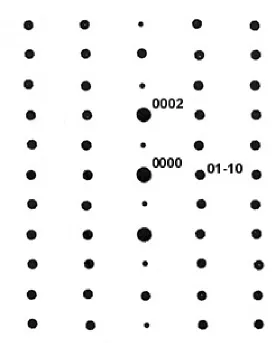
separation of 49% In composition. (Piner) ...61 Figure 4-8 TEM – SAD image showing 10% In InGaN alloy. TEM pattern shows
[2-1-10] zone axis. Notice how spots are clearly defined without any additional
spots. ...62 Figure 4-9 TEM – SAD image showing 49% In InGaN alloy. TEM pattern shows
[2-1-10] zone axis. Notice how the spots are split for higher indexes indicating phase separation of the InGaN alloy. Vertical smears in the c-axis (vertical
direction) are stacking faults...63 Figure 4-10 Behaviour of different InGaN alloys compared with predicted solubility.
Figure 4-11 Cross-sectional TEM image of 20% InGaN film. No phase separation is observed. The arrows indicate the ordered regions. Both 1:1 and 1:3 In:Ga
ordered regions are observed. ...65 Figure 4-12 Cross-sectional TEM image of 49% InGaN showing both phase
separation and ordering. Dark regions are high In phase, while arrows indicate ordered regions...66 Figure 4-13 TEM-SAD image of 20% InGaN film showing extra spots due to both
1:1 (50%) and 1:3 (25%) ordering. Inset shows magnified view of extra spots...67 Figure 4-14 TEM-SAD image of 49% InGaN film showing extra spots due to 1:3
(25%) ordering. Inset shows magnified view of extra spots...68 Figure 4-15 Schematic diagram showing the ordering structures for 1:1 and 1:3 In:Ga
ordering along the c-axis...69 Figure 4-16 Summary of runs checked by TEM for ordering ...70 Figure 4-17 Cross-sectional TEM image of 20% InGaN showing ordered region near
edge of crystal domain. Arrow indicates threading dislocation. The right image shows magnified view of ordered region. Both 1:1 and 1:3 In:Ga ordering are present...71 Figure 4-18 Computer generated theoretical TEM-SAD pattern for perfect 1:1
ordering of InGaN crystal. Smaller spots are extra spots due to ordering...72 Figure 4-19 Computer generated theoretical TEM-SAD pattern for perfect 1:3
ordering of InGaN crystal. Smaller spots are extra spots due to ordering...73 Figure 4-20 TEM-SAD image of 14% AlGaN showing 3:1 Ga:Al ordering along the
Figure 4-21 Simulated diffraction pattern for [2-1-10] zone axis...75 Figure 4-22 Schematic of a twin plane. ...76 Figure 4-23 Wuff net construction for generating virtual twin plane for [2-1-11] twin.
The dark line indicates where reverse twin of image plane would be located.
Circles represent spots that can be twinned to image plane...77 Figure 4-24 Computer generated simulated TEM-SAD image with additional spots
added from Wuff net construction for [2-1-11] twin represented by a 35° rotation around [01-10]. The extra spots from the twin are indicated by hollow circles. ...78 Figure 4-25 Wuff net construction for generating virtual twin plane for [2-112] and
[-1012] twins. Lines indicate where reverse twins of image plane would be
located. Circles represent spots that can be twinned to image plane. ...79 Figure 4-26 Computer generated simulated TEM-SAD image with additional spots
added from Wuff net construction for [2-1-12] twin represented by a 65° rotation around [01-10]. The extra spots from the twin are indicated by hollow circles. ...80 Figure 4-27 Computer generated simulated TEM-SAD image with additional spots
added from Wuff net construction for [-1012] twin represented by rotation around the [1-210]. The extra spots from the twin are indicated by hollow
circles. ...81 Figure 4-28 Computer generated simulated TEM-SAD image with additional spots
Figure 4-29 TEM image compared with same region imaged using extra ordering spots. Ordered regions are enhanced, showing that extra spots are coming from ordered regions indicated by arrows ...83 Figure 4-30 Simulated diffraction pattern using Fourier transform of TEM image of
20% InGaN alloy. Fourier transform of the image gives same pattern as TEM-SAD...84 Figure 5-1 Structure for AlInGaN Growth using GaN buffer layer ...99 Figure 5-2 Plot of growth flux required for 10% InGaN at various temperatures.
In:Ga ratio was held constant at 10:1 while V/III ratio was 100,000:1 (Aumer) ....100 Figure 5-3 Cross-sectional TEM of the self-assembled superlattice (SASL) in
AlInGaN. The SASL consists of high-In, high-Al regions alternating with lower-Al, lower-In regions. The arrows are pointing to the bright layers with
high-Al and high-In content...101 Figure 5-4 SIMS data for SASL shows increase in both In and Al during SASL effect.
In increases from 6-9% while Al increases from 8-23%. Temperature and
Growth conditions are constant. ...102 Figure 5-5 Quantum well structure exhibiting SASL effect. Quantum well is 6nm
InGaN while cladding layers are AlInGaN with SASL...103 Figure 5-6 Graph shows actual and predicted 0002 lattice spacing for constant In
incorporation and Strain Equilibrium In incorporation at 790°C. In:Al ratio for Strain Equilibrium. Effect is approximately 1:4.5 for growth on GaN. The
Figure 5-7 Graph shows actual and predicted 0002 lattice spacing for constant In incorporation and Strain Equilibrium In incorporation at 810°C. In:Al ratio for Strain Equilibrium Effect is approximately 1: 4.5 for growth on GaN. The
datapoints closely follow Strain Equilibrium Effect curve...105 Figure 5-8 Graph shows actual and predicted 0002 lattice spacing for constant In
incorporation and Strain Equilibrium In incorporation at 830°C. In:Al ratio for Strain Equilibrium Effect is approximately 1: 4.5 for growth on GaN. The
datapoints closely follow Strain Equilibrium Effect curve...106 Figure 5-9 Graph shows actual and predicted 0002 lattice spacing for constant In
incorporation and Strain Equilibrium In incorporation for 857°C. In:Al ratio for Strain Equilibrium Effect is approximately 1: 4.5 for growth on GaN. The
datapoints closely follow Constant In incorporation curve. ...107 Figure 5-10 Plot shows suppression of phase separation with increasing Al content.
The strain from Al cancels strain from In reducing the strain and the driving
force for phase separation. ...108 Figure 5-11 Structure for critical layer thickness study. Thin InGaN layers are grown
on 1µm GaN bulk layer. Buffer layer is GaN buffer layer. ...109
Figure 5-12 Results for critical layer study showing the critical layer thickness for
different InGaN compositions...110 Figure 5-13 Reciprocal lattice maps for InGaN samples. Maps show main layers at
Figure 5-14 Double crystal X-ray analysis of 11-24 off axis peak to determine
composition. 25 minute film shows composition of 4.2% InGaN (Reed)...112 Figure 5-15 Double crystal X-ray analysis of 11-24 off axis peak to determine
composition. 105 minute film shows composition of 6.2% InGaN(Reed)...113 Figure 5-16 Results from Gong, et al., showing the increase of Al composition for
AlGaN grown on AlN layer compared with AlGaN grown on a GaN layer.
Shows similar composition pulling effect in AlGaN (Gong) ...114 Figure 5-17 Two-dimensional Valence Force Field Model showing In1Al1Ga62N
crystal atom positions are distorted by the strain fields surrounding the In and Al atoms. The total strain Energy of the crystal is 20.01 arbitrary units. ...115 Figure 5-18 Two-dimensional VFF model of same In1Al1Ga62N crystal as before but
with the In and Al atoms moved closer together. The strain fields from the In and Al atoms cancel out leaving the surrounding atoms relatively undistorted. The total strain for the crystal is 15.32 arbitrary units...116 Figure 6-1 Calculation of phase diagram using the regular solution model. Ω used is
Stringfellows value of 5.98 kcal/mol. Upper curve represents the strain energy H. Lower curve represents the entropy term TS. ...127 Figure 6-2 Calculation of phase diagram using the regular solution model. Ω used is
Stringfellows value of 5.98 kcal/mol. Upper curve is the free energy diagram. Lower curve is the derivative of the free energy. ...128 Figure 6-3 Predicted phase diagram for InGaN from Ho and Stringfellow (APL 69
Figure 6-4 Formula for Delta Lattice Parameter model with table of interaction
parameters for III-V alloys...130 Figure 6-5 Limiting cases for the VFF model. The VCA approximation represents
fixed bond angles, while the CRA approximation represents fixed bond lengths. The minimum energy VFF model is a combination of the two but is closer to the CRA model. ...131 Figure 6-6 Figure showing the actual bond lengths for the InGaN crystal system. The
upper and lower lines represent the CRA crystal approximation and the middle line represents the VCA approximation. Figure from Jeffs N.J., Mater. Res. Soc. Symp. Proc. No 512, p.519. ...132 Figure 6-7 Diagram of the stretching and bending moments for the GaN tetrahedra
used in the VFF model. α represents the bond stretching energy and β
represents the bond angle distortion ...133 Figure 6-8 Formula for the VFF model in the zinc-blende crystal system. The rij
represent the vectors between the pairs of atoms in the tetrahedra. The atom
position is relocated to get a minimum total energy U ...134 Figure 6-9 Elemental clusters used for the CVM method. The cluster variation
method statistically combines the elemental clusters and was used extensively in the zinc-blende crystal structure as the basis for the DLP model ...135 Figure 6-10 The cluster variation method has drawbacks however. If alloy is 25%
overall, 0%, 50%, 75% and 100% tetrahedral will all be strained leaving only
Figure 6-11 Phase diagram for the AlInGaN system showing isotherms from 0-3000C Figure from Matsuoka T., Apl. Phy. Lett. 71 (1) 1997 ...137 Figure 7-1 Diagram of the stretching and bending moments for the wurtzite GaN
tetrahedra. Note that the distances in the a and c directions are not equal. Likewise, the angles between the a-a and a-c bonds are not equal either. This
makes the calculations more difficult. Figure from Takayama. ...170 Figure 7-2 Formula for the total energy for the wurtzite VFF model. Notice that the
c axis components and a axis components have be calculated separately. This is essentially the algorithm used for the current model; however, the axis have been transformed to a orthogonal axis system to allow the use of dot products instead of the slower cos() functions. Figure from Takayama...171 Figure 7-3 Comparison of the current model to the data from Takayama. The values
are in agreement to less than 5%. Because both models are randomly generated, perfect agreement is unlikely...172 Figure 7-4 Showing the convergence of the strain energy with iterations for 25%
InGaN alloy using the VFF model. Bottom plot is same curve on a magnified
scale...173 Figure 7-5 Showing strain energy vs. number of iterations for 25% InGaN alloy.
Notice that the final converged value is not the minimum. This is due to the
greedy algorithm being non-optimal...174 Figure 7-6 Table showing the final values of strain energy for different threshold
Figure 7-7 Plot of Ω vs. composition for the wurtzite VFF model. Adding In to a
GaN matrix is more difficult than adding Ga to an InN matrix due to the larger strain energy for GaN...176
Figure 7-8 Free energy curves using variable Ω. Notice once again the lower
solubility of In in the GaN matrix...177 Figure 7-9 Calculation of phase diagram using the regular solution model.
Stringfellows value for Ω of 5.98 kcal/mol is used. Upper curve is the free
energy diagram. Lower curve is the derivative of the free energy...178 Figure 7-10 Unstable mixing region calculation for AlInGaN from Takayama. ...179 Figure 7-11 Calculated Spinodal for AlInGaN from Matsuoka ...180 Figure 7-12 Free energy curves, for the relaxed crystal, generated using the VFF
calculation at every point. Model used code from Monte Carlo algorithm, but
with random swaps. Values for InGaN (0 Al) curve are consistent with Ω
calculations. Notice the decrease in In solubility with increasing Al. ...181 Figure 7-13 Derivative of the free energy curve for relaxed crystal. Notice the
decrease (x axis intercept) of the equilibrium In composition. Spinodal point
(maximum) is relatively unaffected. ...182 Figure 7-14 Free energy curves for strained InGaN and AlInGaN on GaN generated
using the VFF calculation for every point. Model used code from Monte Carlo algorithm, but with random swaps. Notice that unlike the relaxed curves the
Figure 7-15 Derivative of the free energy curve for strained InGaN and AlInGaN alloys. The equilibrium In composition increases slightly with increasing Al.
The spinodal point is no longer present. ...184
Figure 7-16 Data from Hiramatsu showing the increase in In composition with layer thickness...185
Figure 7-17 Diagram of the growth of 20% InGaN on a AlGaN layer. The initial layers are strained to the underlying substrate and are of lower composition than the relaxed bulk film...186
Figure 7-18 Method for testing the Monte Carlo In incorporation hypothesis. The two films are compared using the VFF model. The model compares the energy to add an In atom into each film using the relationship ...187
Figure 7-19 Calculations for composition pulling of 20% InGaN on GaN...188
Figure 7-20 11-24 off-axis DCXRD scan of InGaN Showing 4.2% In...189
Figure 7-21 11-24 off-axis DCXRD scan of InGaN Showing 6.2% In...190
Figure 7-22 Composition pulling calculations of 6.2% InGaN on GaN...191
Figure 7-23 Showing the standard deviation for ten runs with the Boltzmann probability applied to the addition of In atoms only. The deviations using this method are large enough to mask the Strain equilibrium In incorporation effect...192
Figure 7-24 Start the Monte Carlo algorithm by calculating the strain energy of the crystal...193
Figure 7-25 Select two random column III sites that are different atoms and exchange positions. ...194
Figure 7-27 If the energy is less, the swap always occurs. If the energy is greater then the probability is given by the formula P = Exp(-(Energy change)/kT).
Unfavourable transitions are still possible but with a Boltzmann distribution of probability...196 Figure 7-28 Monte Carlo simulation for Al1In1Ga126N showing the final number of
atoms per lattice site vs. strain energy of that lattice site. Simulations are run for various numbers of sweeps. ...197 Figure 7-29 Monte Carlo simulation showing the final number of atoms per lattice
site vs. strain energy of that lattice site. Simulations are run for various numbers of sweeps...198 Figure 7-30 Monte Carlo simulation showing the final number of atoms per lattice
site vs. strain energy of that lattice site. Simulations are run for various numbers of sweeps...199 Figure 7-31 Monte Carlo simulation showing the final number of atoms per lattice
site vs. strain energy of that lattice site. Simulations are run for various numbers of sweeps...200 Figure 7-32 Plot of the correlation coefficient R to the ideal Boltzmann distribution.
Curve is essentially flat above 32 sweeps. Curve bends over between 16 and 32 sweeps. Therefore all simulations will be run at least 25 sweeps...201 Figure 7-33 The minimum energy location has a path of two bonds between the In
Figure 7-34 Curves showing Monte Carlo simulation of Al1In1Ga126N crystal at 300K
and 300°C. The number of atoms per lattice site is plotted vs. strain energy of lattice site. ...203 Figure 7-35 Curves showing Monte Carlo simulation of Al1In1Ga126N crystal at
500°C and 700°C. The number of atoms per lattice site is plotted vs. strain
energy of lattice site...204 Figure 7-36 Curves showing Monte Carlo simulation of Al1In1Ga126N crystal at
800°C and 900°C. The number of atoms per lattice site is plotted vs. strain
energy of lattice site...205 Figure 7-37Curves showing Monte Carlo simulation of Al1In1Ga126N crystal at
1000°C and 1200°C. The number of atoms per lattice site is plotted vs. strain
energy of lattice site...206 Figure 7-38 Curves showing Monte Carlo simulation of Al1In1Ga126N crystal at
1400°C. The number of atoms per lattice site is plotted vs. strain energy of lattice site. Notice how the curve fits the Boltzmann less and less at high
temperatures...207 Figure 7-39 Plot of correlation coefficient of the data to the ideal Boltzmann
distribution. Note the second order transformation between 800°C – 900°C. This is most likely due to the increase in thermal energy allowing the atoms to hop “uphill” against the strain field. ...208 Figure 7-40 Curve showing strain energy and integrated differential strain energy for
the Monte Carlo simulation of a 25In 25Al 78Ga N alloy. Convergence is
Figure 7-41 Curve showing strain energy and integrated differential strain energy for 5In 5Al 118Ga N alloy. Notice the much faster convergence than the 25In 25Al alloy...210 Figure 7-42 Free energy curve for Monte Carlo simulation for 128 atom AlInGaN
crystal strained to GaN at three different compositions of Al. Simulation was run at 800C for 25 sweeps. The equilibrium In composition increases with
increasing Al. Simulation runs took approx. 20hr. ...211 Figure 7-43 Derivative free energy for Monte Carlo simulation of 128 atom AlInGaN
crystal strained to GaN. Equilibrium In composition shifts from 2.5In to 7In with the addition of 25Al atoms. This is in complete agreement with the strain equilibrium In incorporation effect...212 Figure 7-44 Monte Carlo simulation for 1024 atom crystal strained to GaN at three
different compositions of Al. Simulation was run at 800C for 10 sweeps. The equilibrium In composition increases with increasing Al, but not as large an
effect as for 128 atoms. Simulation runs took approx. 20 days...213 Figure 7-45 Derivative free energy for Monte Carlo simulation for 1024 atoms
strained to GaN. Equilibrium In composition shifts from 22In to 44In with the addition of 200Al atoms. The expected shift would be 40In. The discrepancy between the actual and expected shift is due to the limited number of sweeps...214 Figure 7-46 Set of Monte Carlo runs for 25Al curve. Monte Carlo simulations were
that the discrepancies for the 1024 atom crystal are from an insufficient number of sweeps...215 Figure 7-47 Derivative free energy for Monte Carlo simulation for 25Al curve. The
25 sweep curve matches the results for the 128 atom simulation while the 5 sweep is in close agreement with the 1024. This would indicate that the discrepancies for the 1024 atom crystal are from an insufficient number of
sweeps...216 Figure 7-48 Free energy curves from Monte Carlo simulation for 128 atoms strained
to GaN at 1000°C and 25 sweeps. The equilibrium In composition changes from 5In to 10In. While the equilibrium In compositions are higher, the strain
equilibrium effect is unchanged...217 Figure 7-49 Derivative free energy for Monte Carlo simulation at 1000°C.
Equilibrium In composition shifts from 5In to 10In. All equilibrium In
compositions are shifted higher. ...218 Figure 7-50 Plot of desorption rate vs. temperature for different H2 flows using the
data from the InGaN runs for the H2 study. All fitting curves are normalized to a
Do value corresponding to the Debye frequency for GaN. Resulting activation energy for 0 sccm H2 is 2.6eV. ...219
Figure 7-51 The ratio of diffusion events to desorption events is plotted using the activation energy for desorption combined with the activation energy for In surface diffusion from Neugebauer. The curve is normalized for 1000 diffusion events/ desorption event at 800°C. The number of diffusion events per
Chapter One: Introduction
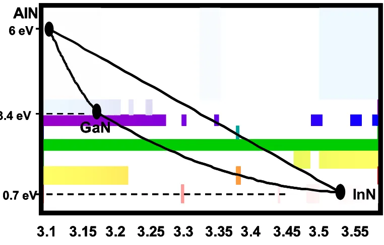
The GaN AlN InN crystal system is a direct bandgap system covering the entire visible spectrum (Figure 1-1). The bandgaps range from 0.8 eV for InN[1] to 3.4 eV for GaN and up to 6.4 eV for AlN[2]. In addition to the optical properties of the nitride materials system, it also has excellent electrical properties. The direct bandgap, a high dielectric strength and good thermal conductivity make the Nitride system ideal for high frequency high power devices. InGaN/GaN Light Emitting Diodes (LEDs) have been commercialized with excellent efficiency in the blue and green[3], allowing for solid-state displays with excellent brightness and contrast. With their 80% electrical power reduction and 1000% lifetime increase over filtered light bulbs, green LEDs are making their way into every stoplight[4]. With the commercialization of GaN based lasers the capacity of optical storage is set to make a giant leap over existing 670nm lasers for DVD.
1.1 Growth of GaN InGaN and AlGaN
The first GaN research was undertaken by Pankove in the early 1970’s[5]. While the devices were grown polycrystalline and had only n-type doping, Pankove was able to achieve detectable light emission using a Metal Insulator Semiconductor structure[6]. A resurgence in the GaN field occurred in 1986 when Amano et al. were able to grow GaN single crystals on Sapphire using a low temperature buffer layer[7]. This led to a burst of research
characterizing the GaN/AlN/InN system. The last hurdle was jumped when Asaki discovered that electron beam annealing could activate Mg doped GaN and make it
p-type[8]. With the ability to p-type dope GaN, the first LEDs were produced in less than three years[9].
1.2 GaN based electronic devices
The combination of high bandgap and high saturation velocity are ideal for high-speed transistors and FETS. The mobility of GaN increases as the layer thickness decreases reaching peak mobility of 600 cm2/Vs at 200Å[4]. To take advantage of this property, Heterojunction Field Effect Transistors (HFETs) are used. Using this structure, room temperature mobilities of 1650 cm2/V s have been achieved. Using the High Electron Mobility Transistor (HEMT) structure two-Dimensional electron gas mobilities of 2200cm2/Vs have been achieved[10]. GaN HEMT have been demonstrated with cut-off
frequencies of 140GHz[11]. GaN/AlGaN Heterojunction Bipolar Transistors (HBTs) have been demonstrated with power densities of 270kW/cm2 [12].
1.3 GaN based optical devices
Before the advent of GaN based LEDs the colors commonly available for LEDs were bright red, bright yellow, and a pale yellowish green. While efficiencies of red and yellow LEDs were pushing 40% efficiency, the green LEDs based on GaAsP were not able to get above 0.1% efficiency in the 530nm green range, the wavelength for the eyes peak
sensitivity. This is due to the GaAsP semiconductor becoming indirect at those wavelengths. As disappointing as that might sound, it was great compared to the only commercially
available blue LED based on a transition level in SiC. The SiC based LEDs (not to be
confused with the GaN LED grown on SiC which are extremely efficient) cost several dollars apiece and had an efficiency of 0.02%[4]!
with existing highly efficient red and yellow LEDs, whole new applications using solid-state lighting are now possible.
1.4 Laser Diodes
The emergence of commercially viable blue Laser Diodes (LD) opened up a whole new era in optical storage. While the CD standard used GaAs based LD at 800nm to store 700MB of information on an optical disk, InGaAsP LD at 670nm can store 4.7 GB on the same sized optical disk. With the introduction of InGaN based LD at 405nm, the blue-ray optical disks are expected to make a similar leap in capacity. In fact, the improvement in areal density combined with closer track spacing and multiple layers has led to the development of optical drives holding 100GB on a single CD.
Current GaN based LD are operating at threshold currents of 2000A/cm2 with quantum efficiencies of 35%[15]. Compare these numbers to the current red and infrared LD with 500A/cm2 [16] and 80% quantum efficiency. While the blue lasers might not appear in walkmans anytime soon, they have reached the power, efficiency, and reliability to be a commercial success.
1.5 Quantum Dots in InGaN
1.6 References
1. Wu, J., et al., Unusual properties of the fundamental band gap of InN. Applied Physics Letters, 2002. 80(21): p. 3967-3969.
2. Morkoc, H., et al., Large-Band-Gap Sic, Iii-V Nitride, and Ii-Vi Znse-Based Semiconductor-Device Technologies. Journal of Applied Physics, 1994. 76(3): p. 1363-1398.
3. Nakamura, S., et al., Characteristics of InGaN multi-quantum-well-structure laser diodes. Applied Physics Letters, 1996. 68(23): p. 3269-3271.
4. Nakamura, S., The blue laser Diode. 1997: Springer.
5. Pankove, J.I., et al., Luminescent Properties of Gan. Solid State Communications, 1970. 8(13): p. 1051-&.
6. Pankove, J.I., E.A. Miller, and Berkeyhe.Je, Gan Electroluminescent Diodes. Rca Review, 1971. 32(3): p. 383-&.
7. Amano, H., et al., Metalorganic Vapor-Phase Epitaxial-Growth of a High-Quality Gan Film Using an Ain Buffer Layer. Applied Physics Letters, 1986. 48(5): p. 353-355.
8. Amano, H., et al., P-Type Conduction in Mg-Doped Gan Treated with Low-Energy Electron-Beam Irradiation (Leebi). Japanese Journal of Applied Physics Part 2-Letters, 1989. 28(12): p. L2112-L2114.
9. Nakamura, S., Zn-Doped Ingnn Growth and Ingan/Algan Double-Heterostructure Blue-Light-Emitting Diodes. Journal of Crystal Growth, 1994. 145(1-4): p. 911-917. 10. Demchuk, A., et al. MOCVD AlGaN/GaN HFET's Material Optimization and
Devices Characterization. in 2003 FALL MEETING PROCEEDINGS. 2003. 11. Parikh, P., et al., Record power-added-efficiency, low-voltage GOI (GaAs on
12. Makimoto, T., Y. Yamauchi, and K. Kumakura, High-power characteristics of
GaN/InGaN double heterojunction bipolar transistors. Applied Physics Letters, 2004. 84(11): p. 1964-1966.
13. Barsky, F., Cree Expands Green LED Product Family. 2004, Cree.
14. Barsky, F., Cree Expands Product Line With Introduction of XThinTM LED Products. 2003, Cree.
15. Hansen, M., et al., Higher efficiency InGaN laser diodes with an improved quantum well capping configuration. Applied Physics Letters, 2002. 81(22): p. 4275-4277. 16. Li, W., et al., Low-threshold-current 1.32-mu m GaInNAs/GaAs single-quantum-well
lasers grown by molecular-beam epitaxy. Applied Physics Letters, 2001. 79(21): p. 3386-3388.
17. Chichibu, S.F., et al., Emission mechanisms of bulk GaN and InGaN quantum wells prepared by lateral epitaxial overgrowth. Applied Physics Letters, 1999. 74(10): p. 1460-1462.
3.4 eV
3.1 3.15 3.2 3.25 3.3 3.35 3.4 3.45 3.5 3.55
3.6
AlN
GaN
InN
6 eV
0.7 eV 3.4 eV
3.1 3.15 3.2 3.25 3.3 3.35 3.4 3.45 3.5 3.55
3.6
AlN
GaN
InN
6 eV
0.7 eV
3.1 3.15 3.2 3.25 3.3 3.35 3.4 3.45 3.5 3.55
3.6
AlN
GaN
InN
6 eV
0.7 eV
Chapter Two: Experimental Methods
2.1 Metal Organic Chemical Vapour Deposition (MOCVD)/ALE System
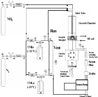
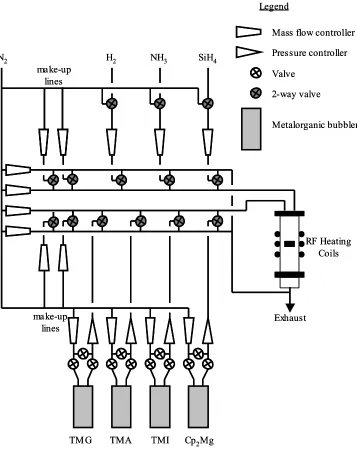
MOCVD growth consists of Chemical Vapour Deposition, a chemical reaction of the component gasses on the surface of the growing film, using metalorganics as the precursor gasses. In MOCVD, the liquid metalorganics are delivered to the gas stream by passing the carrier gas through a bubbler and carrying the carrier gas / metalorganic vapour to the growth surface along with gaseous ammonia. In our reactor design, the Ga, Al, In, and Mg sources are liquid metalorganics in bubblers. The column V sources ammonia (for N) and silane (for Si doping) are delivered by pressurized cylinders of high purity gas.
MOCVD is popular in industry because of its (relatively) low cost and high
throughput. Because the MOCVD is grown at pressures ranging from 100 torr – 750 torr, the chamber does not need to be pumped to high vacuum. The disadvantages of MOCVD are that the incomplete pyrolysis of the metal-organics leads to carbon contamination in the growing films. While having the proper gas conditions during growth can minimize carbon incorporation, it will not totally eliminate it.
2.1.1 Gas delivery system
each bubbler allow for constant flows through the MFC when the bubblers are switched to flowing from bypassed. All of the column III flows and column V gasses are delivered into the run/vent manifold through MFCs at a constant pressure.
The run/vent manifold output runs to two main lines that travel to the chamber and to the vent manifold. For each input gas, there is a pair of pneumatic valves attached to these two main lines. This series of valves (one pair for each incoming gas) switch each flow to either the run or vent line. This allows the gas flows to be stabilized by flowing to the vent line before they are switched. The pressure in the run manifold is determined by a needle valve in the lines leading to the chamber, while the pressure in the vent line can be controlled by either a needle valve or by changing the N flow into the vent manifold. Pressure gauges are mounted at each of the bubblers and in the run and vent manifolds. The pressure of the main growth chamber is controlled by a MKS pressure controller that holds the chamber at a constant pressure by automatically operating a throttle valve at the output of the growth chamber. Since the vacuum pump is always running the chamber pressure can be controlled from very low pressure (limited by the pumping capacity and the growth flows) to above atmospheric (by almost closing the valve).
The system is supplied by ultra high purity N2 that is run through a Nanochem
purifier. The NH3 is supplied from a tank and then run through another Nanochem filter.
Finally, the H2 source is also supplied from a high-pressure cylinder and then run through a
third Nanochem purifier. Each Nanochem purifier is designed for its specific gas. A series of pneumatically controlled three-way valves control the different gas flows leading to the chamber. By operating these valves from the control panel, the outputs of the run line can be switched to the various different inputs on the chamber for the ALE and MOCVD growth modes.
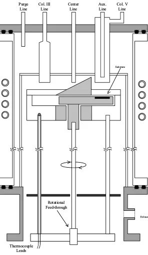
In the MOCVD/ALE system, the growth chamber (Figure 2-2) is constructed of quartz and stainless steel. The main section of the chamber is quartz to allow for Radio Frequency (RF) heating while the top plate and bottom flange are stainless steel. The quartz is sealed to the stainless steel using a double o-ring seal, with a small vacuum pump
evacuating the volume between the o-rings. Large clips are used to hold the quartz tube to the endcap and the flange. The various gas lines are plumbed into the system through the stainless steel top plate. The column III, column V, centerline, and the auxiliary line are all separately controlled, allowing for a large degree of flexibility. The graphite susceptor sits inside another smaller quartz chamber that seals the reaction gasses further from the rest of the chamber.
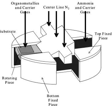
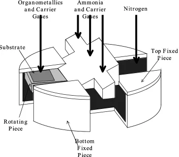
The heart of the MOCVD/ALE reactor is the ALE susceptor. An illustration of the susceptor, showing the gas flows, is given in Figure 2-3. The design of the susceptor is critical to the growth process. The susceptor is constructed of graphite and coated with SiC to protect it from the growth environment. The graphite serves as an inductive load to heat the sample from the RF coils. The susceptor also has to control the flow of gasses in the ALE mode to keep the column III and column V flows separated. The susceptor is
constructed in three pieces. The top plate serves mainly to separate and direct the gas flows. The rotating piece has to both heat and rotate the sample between the column III and column V sides of the growth chamber. Finally, the base of the susceptor has to support the
susceptor in the chamber, mount the thermocouple for temperature measurement, and serve as a bearing surface for the rotating piece. At the bottom of the chamber, a magnetic feed-through is used to rotate the sample, while a bellows is used to allow for raising and lowering the susceptor.
2.2 Thomas Swan MOCVD System
only the changes in design will be given here. For growth of optical devices, abrupt
interfaces are very important. The Thomas Swan reactor has many features that are designed for the instantaneous changes in precursor flux needed for abrupt layers. Because the volume of a valve limits its switching speed, the Thomas Swan run/vent switching block is
constructed of custom valves with very small static volumes.
Another problem encountered when growing abrupt interfaces is the changes in
pressure when gas flows are changed from the vent line to the run line. This problem is fixed by an extra set of make up lines flowing the carrier gas. The make up lines are controlled by the computer to flow an amount of gas corresponding to the switch in flows between the run line and the vent line. If a TMIn line flowing 300 sccm is switched from run to vent, then the vent makeup line will flow 300 sccm and switch from vent to run. The make-up lines, along with the pressure controlled vent MFC keep the pressures in the vent and run line equal under all conditions.
The chamber design for the Thomas Swan (Figure 2-6) reactor is a copy of the final MOCVD chamber design, with the only difference being the input tube. In the
ALE/MOCVD reactor the inlet tube consists of a hollow tube with a quartz divider plate, while in the Swan MOCVD the inlet tube consists of two concentric tubes with the smaller inner tube flowing into column III and the larger outer tube flowing into column V gasses.
2.3 Growth of GaN and development of ALE and MOCVD buffer layers
The preparation of the sapphire samples prior to GaN growth is similar to the procedures for other MOCVD processes. The sapphire starts out as 2-inch wafer with c-plane orientation miscut to (11-20). The samples are cut up into 15mm x15mm squares for use in the MOCVD reactor. This has two purposes, it uses up less sapphire and it also makes the growth uniformity less critical. Growth uniformity varied considerably among the
various chamber configurations. The 15mm x 15mm samples were cleaned in batches of seven samples, which correspond to the number of samples from one two inch sapphire wafer. The samples were cleaned in boiling hexane, acetone, and methanol and then dried with clean N2 from a GP45 liquid cylinder. The cleaned samples were then placed in a dry
box under flowing N2 until they are ready for growth.
The preparation of the growth chamber consisted of a cycle purge that involved
opening the throttle valve to pull to the lowest pressure allowed and then setting the pressure to 100 torr (later 150 torr). This process was repeated 10 times using a relatively high flow of N2. This cycle purge was performed right after the sample was loaded before the growth
run was started. If the prior run were an InGaN run, the chamber would be coated with In from the previous run. This required a bake-out run without a sample present to remove some of the In from the walls of the chamber. The bake-out run was performed at 1000°C and maximum flow of H2.
In the initial stages of the growth run, after the cycle purge, but before any of the reactant gasses were flowed, a preclean step was performed using 1050°C and 15 minutes of maximum H2 flow. This served to remove any organic material from the surface of the
sapphire wafer. This preclean step was eventually performed at 1100°C as the susceptor/RF coupling was improved to allow higher temperatures. After the preclean step, the sample is ready for growth.
layer growth process was used. This involved a passivation step introducing NH3 at high
temperature for a short period of time (typically 1 min).
After the passivation step, the AlN buffer layer is grown using the system in the ALE growth mode (Figure 2-3). This configuration consisted of the susceptor utilizing a rotating and stationary component. This allowed both MOCVD and ALE growth with the same susceptor. In the ALE mode, the sample is mounted on a rotating portion of the susceptor and then gasses are flowed such that the column III gases consisting of TMAl with a N2
carrier gas are flowed in at the front of the susceptor, the column V gasses consisting of NH3
and a N2 carrier gas are flowed in the back of the susceptor, and a centerline flow is run in
the center three tubes to separate the column III and column V gas flows. The sample is rotated at 30 RPM so that the sample alternates between the column III and column V gas flows every two seconds. Combined with the c-plane orientation of the sample, this has the effect of growing one monolayer at a time on the growth surface. The ALE growth is continued for 500 Al-N monolayers.
For growth utilizing the MOCVD GaN buffer layer, the thermal clean and passivation steps are performed the same as for the ALE buffer layer. After the passivation step, the sample is cooled to the GaN buffer layer growth temperature. Growth temperatures from 500°C to 600°C were used in the study to improve GaN buffer layer quality. The sample is allowed to rest at the GaN buffer temperature and then, when the temperatures have
stabilized, the GaN buffer layer is grown. The GaN buffer layer is grown at GaN flow rates from 3.5 – 5.0 sccm to give a thickness ranging from 3.0 – 6.0 Å per second. NH3 flows
ranged from 1.0 - 1.25 l/m, giving a V/III ratio of 4000 to 7200. The thickness and temperature of the buffer layer were changed in an effort to improve the properties of the final GaN film.
After the growth of the GaN buffer layer, the sample was heated up to the growth temperature for the main GaN growth layer. The combination of gas flow conditions and ramp rate were important factors for the quality of the bulk GaN film that was grown afterwards. The growth conditions for the bulk GaN layer were changed from the buffer layer. The growth flux was lowered to 1.0 – 3.0 sccm, resulting in a V/III ratio of 6700 to 25000.
If the sample is grown too thick, the sample may crack during cool-down due to the thermal mismatch. The thickness at which cracking occurs depends on the combination of the composition and thickness of the bulk film. Even identical compositions vary in the susceptibility to cracking depending on the growth quality of the film. Films that have a finely nucleated buffer layer and high dislocation density are more susceptible to cracking than the films that were grown with a sparsely nucleated buffer and lower dislocation density.
One of the best measurements of crystal quality both chemically and structurally is the Hall measurement. The Hall measurement setup consists of a large electromagnet controlled manually combined with computer controlled digital multi-meter and programmable current source. The samples are cleaved into a 5mm by 5mm square pieces and then cleaned in acetone and methanol. The contacts consisted of In dots that had been carefully cut from a block of In using a fresh razor blade and then chemically cleaned in HCl for 30 seconds to remove any impurities. The In dots are then rinsed with de-ionized water and methanol and then stored in a beaker filled with methanol.
The GaN samples were mounted in a temperature controlled mounting stage. The stage can be either heated resistively or cooled using adiabatic expansion of high pressure N2.
The temperature range for the Dewar was 77K to 373K. The sample was connected to Keithly instruments that were under computer control. The computer program used the Van der Pauw technique to calculate the sheet resistance, resistivity, carrier concentration, and the mobility of the sample.
The background concentration of the samples gave a good indication of the quality of the crystal. The samples grown with insufficiently thick buffer layers exhibited poor crystal quality. In addition to the poor double crystal XRD full width half maximum, these samples had background concentrations above 1018 and mobilities less than 100 cm2/V s. Samples grown with optimized buffer layers had carrier concentrations in the low 1017 and mobilities
of almost 290 cm2/V s. Later work by Mason Reed with GaN buffer layers optimized for H 2
carrier gas resulted in mobilities of almost 400 cm2/V s.
2.5 Photoluminescence
Photoluminescence (PL) was used to determine the optical properties of the material. While Hall mobility is affected by all kinds of defects, PL mainly responds to optically active defects. For poor quality (either chemically or structurally) crystals, the photoluminescence is weak and corresponds to a deep level with the photon energy below the bandgap. These deep levels result from optically active impurities. A good example of this is the weak yellow emission from InGaN containing carbon impurities. This yellow deep level peak is present due to the incomplete reaction of the metalorganics from low temperature, low H2
partial pressure or a combination of both. The presence of optically active defects is very important to the operation of optical devices. In our experiments, PL is mainly used to characterize InGaN and AlGaN layers used in LED structures. For the InGaN layers, PL can give the optical bandgap of the material, which may, or may not, be at the band edge. By looking at the intensity and line width of the InGaN peak, it is possible to determine the optical quality of the films. PL is usually combined with θ-2θ x-ray analysis to determine the composition of InGaN films.
PL can also be performed on AlGaN/InGaN/AlGaN quantum well structures to determine the quality of the quantum well. Quantum wells are very sensitive to the barrier height and well width, therefore it is necessary to optimize these conditions to get an efficient device. By comparing quantum wells with identical structures grown at earlier times it is possible to check the system for contaminants that would affect optical devices. Because the quantum well concentrates the carriers in a small region, the output from quantum wells is much more susceptible to optically active defects than the bulk crystal.
a chopper that pulses the beam in sync with a lock-in amplifier. The chopped beam is
focused to hit the sample at an angle, allowing both the reflected and transmitted beam of the pump laser to be blocked. The spot at which the pump laser strikes the sample is imaged by a second set of optics to image the luminance from the sample. The luminance signal is filtered to block any scattered light from the pump laser. The luminance signal is then run through a motorized diffractometer. Slits at the input and output of the diffractometer determine the sensitivity when output to the photomultiplier tube. By measuring samples with consistent slit settings and photomultiplier voltages, it was possible to compare the relative intensity of different quantum wells.
2.6 θ –2θ x-ray analysis.
The θ-2θ x-ray was used to determine the InGaN and GaN (0002) peaks. The θ -2θ
x-ray machine is a Rigaku system set up for Cu Kα radiation (λ = 1.54058) at 35kV and 25mA of beam current. Samples were scanned from 15° < 2θ < 80° at 0.02 degrees per second. For higher sensitivity, when looking at thin films or looking for forbidden peaks, a longer count time was used. The samples were calibrated to the c-plane (0006) sapphire peak located at 2θ = 41.685°. The GaN and InGaN peaks are indexed from the sapphire reflection and Vegards law is used to determine the In composition in bulk layers. The Rigaku can also be used to detect phase separation by detecting secondary phases and to detect ordering by the appearance of forbidden peaks. The Rigaku is limited when evaluating strained films due to the (0002) dimension being distorted by the biaxial strain.
2.7 Double crystal XRD
measurement. The resolution of the θ steeper motor is one arcsecond. The DCXRD is used for estimation of crystal quality by measuring the Full Width Half Max (FWHM) of the resulting films. Since the detector is wide open and has no slits, it does not have the resolution to measure composition; however, it can give an indication of the film thickness from the area under the curve. The stage is also motorized to move parallel to the crystal surface allowing a scan over the entire sample to determine film uniformity. These scans were critically important when developing the reactor configuration, as they were the only reliable gauge of growth uniformity. Both on-axis scans and off-axis scans are possible using the DCXRD. By looking at higher order on-axis and off-axis scans, it is possible to determine the compositions of strained thin films. The on-axis DCXRD is not sensitive to threading dislocations that are perpendicular to the surface, while the off axis DCXRD is sensitive to threading dislocations. The off axis measurement is significantly more difficult to perform, limiting its everyday use.
2.8 TEM Analysis
Transmission Electron Microscopy (TEM) was used to characterize the structural quality of the films via high-resolution imaging. TEM was also used to gather
crystallographic information from small regions of the sample using selected area diffraction (SAD). TEM required that the films be prepared to make them thin enough to transmit electrons. A Topcon EMB002 transmission electron microscope at 200kV was used for the TEM studies using two-beam bright and dark field imaging and SAD. Bright-field imaging is performed by collecting information only from the central beam using the objective
2.9 SIMS Analysis
Secondary Ion Mass Spectrometry (SIMS) was utilized to measure the elemental concentration as a function of depth. This is a mass spectrometry technique that involves sputtering material by bombarding the surface with energetic Ce ions, then measuring the secondary ions for the number of atoms of the target element as a function of sputtering depth. Since sputtering rates differ widely a sample of a similar compound of known
Col. V Line Purge
Line
Col. III Line
Center Line
Aux. Line
Rotational Feed-through
Thermocouple Leads
Exhaust Substrate
Col. V Line Purge
Line
Col. III Line
Center Line
Aux. Line
Rotational Feed-through
Thermocouple Leads
Exhaust Substrate
Cen ter Lin e N2
Su bstra te
Bottom F ixed
P iece
Top F ixed P iece
Rota tin g P iece
Orga n ometa llics a n d Ca rrier
Ga ses
Ammon ia a n d Ca rrier
Ga ses
Cen ter Lin e N2
Su bstra te
Bottom F ixed
P iece
Top F ixed P iece
Rota tin g P iece
Orga n ometa llics a n d Ca rrier
Ga ses
Ammon ia a n d Ca rrier
Ga ses
Nitrogen
Su bstra te
Bottom F ixed
P iece
Top F ixed P iece
Rota tin g P iece
Orga n ometa llics a n d Ca rrier
Ga ses
Ammon ia a n d Ca rrier
Ga ses
Nitrogen
Su bstra te
Bottom F ixed
P iece
Top F ixed P iece
Rota tin g P iece
Orga n ometa llics a n d Ca rrier
Ga ses
Ammon ia a n d Ca rrier
Ga ses
Mass flow controller Pressure controller Valve
2-way valve
Metalorganic bubbler
Exhaust
RF Heating Coils N2 H2 NH3 SiH4
TMG TMA TMI Cp2Mg
Legend make-up
lines
make-up lines
Mass flow controller Pressure controller Valve
2-way valve
Metalorganic bubbler
Exhaust
RF Heating Coils N2 H2 NH3 SiH4
TMG TMA TMI Cp2Mg
Legend make-up
lines
make-up lines
exhaust thermocouple rotation arm
RF co ils double o-ring seal
(dry pump for dead volume)
concentric tubes: outer – column V inner – column III
exhaust
baffle inner quartzsleeve top plate (water cooled) bottom plate (water cooled) outer quartz chamber
two piece susceptor: upper – rotating lower – stationary
Chapter Three:Development of GaN Buffer Layer
3.1 Introduction to the nitride buffer layer.
Buffer layers were developed to allow for the growth of single crystal GaN on
sapphire. Sapphire has a lattice mismatch of 15% with GaN, making the growth of a single crystal film very difficult. The solution to this problem is to grow a low-temperature buffer layer that can accommodate some of the mismatch between the sapphire and the single crystal GaN film grown on top of the buffer layer. Growth of GaN on sapphire without a buffer layer results in polycrystalline films that are inferior for electronic and optical devices.
The first buffer layers for GaN grown on sapphire were developed by Amano et al. [1] in 1986. This AlN buffer layer allowed for the growth of single crystal GaN on sapphire. Prior to this point all of the GaN grown had been polycrystalline. The ability to grow single crystal on a inexpensive, readily available substrate gave a significant boost to nitride research and represents one of the milestones in GaN development. With the successful development of the low temperature buffer layer, GaN has been successfully grown on SiC[2], Si[3], and spinel (MgAl2O4)[4]. Growth of GaN on Si represents the lowest possible
cost, but the crystal quality of the resulting GaN film is much poorer than the other
substrates. The growth of GaN on MgAl2O4 is mainly to take advantage of the cleave planes
for making Laser Diodes (LD). The growth of GaN on SiC has been used commercially for many years for LED production. Although the SiC is very expensive compared to sapphire the advantages in processing and packaging from having a conductive substrate more than made up for the cost of the SiC wafers.
Vennegues et al. [5] showed that this AlN layer extended up to 10 monolayers into the
sapphire substrate. After the surface of the sapphire has been passivated, the low temperature buffer layer is grown at between 400°C and 600°C. Growing the buffer layer at a low
temperature results in a highly defective thin film. The crystal defects in the buffer layer serve two purposes. First, they accommodate the mismatch between the GaN and the sapphire. Second, they represent a high-energy crystal state that can recrystallize under annealing. The ramp and anneal step give the low temperature buffer layer time to undergo recrystallization. Finally, the initial growth of the high temperature GaN film is not smooth, but is made up of three-dimensional islands that slowly coalesce into a smooth film.
The quality of the buffer is critical, because the buffer layer determines the polarity of the film, density of stacking faults and mixed polarities, and the dislocation density for all of the films grown afterwards. Traditionally, Ga polar films grow on AlN buffers while N polar films grow on GaN buffers. However, it is possible to get either type of polarity by varying the growth rate of the film[6, 7]. While good quality material has been grown with either polarity, initial buffer layer growth can contain a mixture of both polarities. If the mixture of polarities is not annealed to one or the other, stacking faults will be widespread, thereby reducing crystal quality. The size of the domains in the bulk GaN layer depends on the structure of the underlying buffer layer. Fine domain sizes increase the defect density and reduce the mobility of carriers in the films. Bridger et al. [8] found that the carrier diffusion lengths were proportional to the size of the growth domains. Their data strongly suggest that recombination due to defects at growth domain boundaries is the limiting factor for carrier lifetimes.
competition. The GaN buffer layers had slightly better mobilities at room temperature (450 cm2/V s) than AlN buffer layers[9]. At 77K however, the GaN buffer layers have mobilities
of 900 cm2/ V s. The background carrier concentration is also much lower for GaN buffer
layers than for AlN buffer layers. Carrier concentrations as low as 4 * 1016 have been achieved in GaN on GaN buffer layers[10].
Epitaxial Lateral Overgrowth (ELO) was developed to allow for increased buffer layer performance by laterally growing GaN over a SiO2 mask where the GaN only contacts the
sapphire through openings in the mask[11]. Because the laterally overgrown GaN does not contact the sapphire and is incoherent to the SiO2, the areas of lateral overgrowth have vastly
reduced threading dislocation densities. This gives excellent crystal quality, but with
geometrical limitations due to the masking step. The excellent areas of ELO are in the region between the mask openings and the merger or the two overgrowing layers from the adjacent mask openings. While this structure makes it difficult to generate large area devices, it is ideal for LD as they have a stripe geometry that perfectly matches the geometry of the low defect areas of the ELO Grown Films.
3.2 Growth of The ALE Buffer layer
During my tenure on the MOCVD system, we had grown materials ranging from ALE quantum wells to bulk GaN based on a GaN buffer layer. The first six months on the system were spent with the ALE buffer layer configuration. Most of the work at that time was for the study of H2 on the growth of InGaN alloys. The ALE buffer layer gave good materials
properties for the GaN and InGaN films.
A typical ALE growth run is started by annealing under H2 for 15 minutes prior to
passivation under NH3 for one minute at 1050°C and 700 torr. The temperature is then
the reactor to ALE mode (Figure 2-3), several valves are operated to direct the gas flow to the separate V and III sides used for ALE. The ALE growth was run for 500 cycles with a rotational speed of 30 rpm. After the completion of the 500 cycles of ALE, the reactor is heated to 950°C and growth of MOCVD layers are initiated. During the heat up, the reactor is converted over to MOCVD mode (Figure 2-4). To do this, the column V flow is changed from the back tube to the center tubes that can flow down the ramp. The chamber pressure is increased back up to 700 torr and the sample is rotated and locked under the column III side. The MOCVD layers grown at 950°C consist of a 25% AlGaN layer that is graded to GaN over a period of 2.5 minutes. The AlGaN layer is followed by a GaN prelayer and then by the bulk GaN layer.
The ALE buffer layer had been in use for over a year and had proven to be very forgiving of varying growth conditions. The films were structurally good, with DCRXD linewidths of 40 arcseconds on-axis and 300 arcseconds off-axis. The only problem was that the Hall mobilities were limited to around 290cm2/Vs.
In an attempt to improve upon the ALE buffer layer, we embarked on a series of
system modifications and growth experiments using MOCVD AlN and GaN low temperature buffer layers. Initial experiments utilized the ALE reactor configuration and an AlN buffer layer. Later a hybrid buffer layer utilizing an AlN layer followed by a grading layer to a GaN layer was used. Finally, a pure GaN low temperature buffer layer was used. An extensive series of system modifications were undertaken to transition the chamber from the ALE configuration, which was a compromise between the ALE and MOCVD modes, to a pure MOCVD configuration.
3.3 Development of chamber design
time of the reactants in flux to the growth surface. The initial design for the ALE system used a ramp that served as a divider for the column III and column V gasses in ALE mode and was converted to a guide to route the column V gasses to the growth surface. The problem with this design was that the column V gasses were heated and allowed to diffuse out and slow down as they went down the ramp. These effects increased the likelihood of gas phase reaction in the vicinity of the growth surface.
The initial modification of the system involved the replacement of the paddle for the sample holder with a round disk. This modification required that the ramp be offset to channel gasses from the column V side instead of the centerline. These modifications eliminated the possibility of growing ALE GaN, but allowed for sample rotation for better uniformity and also made the temperature of the sample much more controllable. Although these improvements were beneficial, they still allowed the column III and column V gasses to heat up and react. The best way to reduce this problem was to remove the ramp
completely. This started a series of modifications using bent quartz tubes to channel the gas to the growth surface. Unlike the graphite/SiC ramp used previously, the quartz tubes were not heated by the RF field. This allowed the gasses to remain cooler and be separated until they were close to the sample surface. Unfortunately, we were not able to construct tubes that replicated the smooth transition between the ramp and the sample holder, resulting in turbulence that was detrimental to the film quality.
One of the more serious issues with the system that would cause problems throughout the development of the GaN buffer layer was a consistent “pepper” effect in the films. The “pepper” consisted of small crystals of GaN that were readily apparent by optical
microscopy. At the time, it was decided that the pepper effect was the result of gas phase reaction depositing small crystallites of GaN onto the growing film.
MOCVD growth. Although most of the designs that were tried were unsuccessful, they led to the development of the current setup, which has excellent performance for MOCVD GaN.
The change to the quartz tubes for the column III and column V gasses significantly reduced the heating and intermixing of the reactant gasses, however the samples still exhibited the “pepper”. In addition, the system changes that had been implemented had completely changed the gas dynamics to where all of the previous optimizations were out the window. This resulted in sub-optimum films. In a final attempt to reduce the gas residence time, we modified the quartz tubes to include an additional end plate with dozens of small, laser drilled holes. These holes effectively reduced the cross-sectional area to the limit of the linear flow regime to reduce the gas residence time to the absolute minimum possible.
All of the studies for the optimum design of the column III and column V delivery tubes were done using similar GaN buffer layers. Changes to the growth rate and time had to be made to get consistent results, but the basic temperatures and conditions were held as constant as possible under the conditions. This allows, in a limited way, a comparison between the different gas delivery designs. This was interesting in that the design that had given the best crystal quality was a derivative of the original ALE setup. The optimal
configuration had a sloped pyramid to deliver the column V gasses and a column III tube that had a plate with five medium sized holes in a baffle placed 2 cm from the end of the tube.
The absolute worst setup was the one with the quartz tubes that had laser drilled end caps. It is interesting to note that the design that was intended to have the highest permissible gas velocity to reduce gas phase interaction actually had one of the worst “pepper” surfaces of all of the designs. Hall mobility on the best sample from this design was only 9 cm2/Vs.
incorporated into the current design that uses a long rectangular tube that is at relatively low velocity and utilizes a quartz spacer running down the length of the tube. The current design does have problems with gas phase reaction. However, the solution to this problem was to reduce the chamber pressure, thereby increasing the gas velocity. This proved to be much more effective than using artificial constrictions that induced turbulence.
3.4 AlN Buffer Layers
AlN buffer layers were popular during the early days of GaN, but fell out of favour due to the superiority of the GaN buffer layer. The AlN buffer layer has some of the same
advantages as the ALE buffer layer, namely that there is a wide range of conditions that result in good quality films with smooth specular surfaces. During the AlN buffer layer study, we experimented with buffer layer temperature, growth rate, growth time, and post buffer layer annealing. The optimum conditions that were arrived at were 3 sccm TMGa for 6 minutes with a 3 minute anneal. Unfortunately, the best AlN films that we grew did not have properties that were any better than the ALE buffer layer.
In fact, the MOCVD AlN buffer layer properties were in most cases worse than the ALE. This is an interesting development, as the nitrogen passivation, gas flow, V/III and bulk growth conditions were very similar between the ALE and MOCVD buffer layers. One possible explanation for this is the V/III ratio. Long after we completed the AlN buffer study, Ito et al. [12] reported that the V/III ratio of the AlN buffer layer was critical to the quality of the final film. V/III ratios of less than 1800 were found to give the best quality films. If the V/III ratio is too high, the film quality degrades significantly. Because our AlN buffer layer runs were using a V/III ratio ranging from 4000 to 7200, our conditions were well outside of the ideal range.
This conclusion would seem to be borne out by our results with double the normal NH3