Scholarship@Western
Scholarship@Western
Electronic Thesis and Dissertation Repository
4-18-2017 12:00 AM
Effective Boronizing Process for Age Hardened Inconel 718
Effective Boronizing Process for Age Hardened Inconel 718
Aria KhaliliThe University of Western Ontario
Supervisor
Dr. Robert J. Klassen
The University of Western Ontario
Graduate Program in Mechanical and Materials Engineering
A thesis submitted in partial fulfillment of the requirements for the degree in Master of Engineering Science
© Aria Khalili 2017
Follow this and additional works at: https://ir.lib.uwo.ca/etd
Part of the Metallurgy Commons
Recommended Citation Recommended Citation
Khalili, Aria, "Effective Boronizing Process for Age Hardened Inconel 718" (2017). Electronic Thesis and Dissertation Repository. 4507.
https://ir.lib.uwo.ca/etd/4507
This Dissertation/Thesis is brought to you for free and open access by Scholarship@Western. It has been accepted for inclusion in Electronic Thesis and Dissertation Repository by an authorized administrator of
i
Boronizing or boriding is a technique to mitigate wear damage in industrial
valves made of age-hardenable Inconel
®718 which is a nickel-based
superalloy. Boriding involves immersing the part in a patented boron-based
compound and heating over 800
oC.
Boriding combined with aging has a detrimental thermal effect and was the
subject of this investigation. The effects on hardness, wear and grain size, of
boriding and aging separately, subsequently, and simultaneously, were
investigated to observe the microstructure and mechanical properties.
The results show that boriding has negligible effect on the grain size and the
hardness of the substrate. Besides, a boride coating can improve the surface
hardness by a factor of five and reduce the wear damage by over 75%. As the
wear performance strongly depends on the coating thickness, we found that
initial aging and subsequent boriding delivers the thickest layer and is the best
method for boriding of Inconel
®718.
Keywords
ii
iii
I wish to express my gratitude to Dr. Robert J. Klassen, my supervisor and professor. Being
accepted as a student of Dr. Klassen and working in his group has been an exceptional
honour and a great experience in my academic life. I am grateful for his expert guidance
and the motivation he provided throughout this project, especially at those frustrating times
when I felt deadlocked.
Dr. Klassen’s research group over the past three years has stimulated me in this project and
I would like to extend my sincere thanks to them: Dr. Vineet Bhakhri, Dr. Meysam
Haghshenas, Dr. A. Z. M. Ariful Islam, Heygaan Rajakummar, Md. Imran Khan, Maisaa
Tawfeeq, Feifei Nie, Mahdi Bagheripoor and Lobat Shojaei.
I am thankful for the help and direction from my mentor and friend, Dr. Mehdi Yari at
Surface Heat Treat and Coatings in Hamilton, whom I have known since my undergraduate
years at Azad University in Tehran, and whom has continuously supported me. A special
thanks to the CEO of Surface Heat Treat and Coatings, Mr. John Abrahamse, for allowing
me to use their facilities.
Significant parts of this project were done in the laboratories of my advisors,
Dr. Jeffrey T. Wood and Dr. X. A. (Andy) Sun. I am grateful for their advice and for
permission to use their facilities. I also thank Marc Beauchamp in the Department of Earth
Sciences for assisting me in using their scanning electron microscope (SEM).
I acknowledge the help of many wonderful people in the MME department, especially
Chris Seres, Joanna Blom and Claire Naudi, and support from the Machine Shop, Clayton
Cook and Steve Concannon. Rest in peace Steve; you are always in my memory.
Last but not least, many thanks to all my friends and family who supported me through the
happy and the rough days: Robert Swartman, Toba Mohabbati, Morteza Malekmanesh,
Maryam Ghahremani, Megaraja Elayathamby, Pouria Khalili, Afshan Samani, Pouya
Sharifi, Anibran Banerjee, Babak Razaghi Rad, Elnaz Nouri, Anahita Nouri and my
iv
Abstract ... i
Acknowledgments... iii
Table of Contents ... iv
List of Tables ... vi
List of Figures ... vii
Acronyms ... ix
Symbols ... x
... 1
1 INTRODUCTION ... 1
... 3
2 LITERATURE REVIEW ... 3
2.1 Inconel® 718 Superalloys ... 3
2.1.1 Wear of Inconel® 718 ... 5
2.2 Surface Coatings for Inconel® 718 ... 6
2.2.1 Physical Overlays ... 7
2.2.2 Diffusion Coatings ... 8
2.2.2.1 Boride Diffusion Layers on Nickel Bearing Alloys ... 10
2.2.2.2 Boriding Agents ... 10
2.2.2.3 Structure and Composition of a Boride Coating on a Nickel Alloy ... 12
2.2.2.4 Effect of Alloying Elements on Boride Hardness and Thickness ... 14
2.2.2.5 Effect of Time and Temperature on the Boride Layer Thickness ... 15
2.2.2.6 Wear Properties ... 16
... 17
3 EXPERIMENTAL PROCEDURE ... 17
3.1 Thermal Treatments ... 18
3.1.1 Aging Treatment ... 18
3.1.2 Boriding Treatment ... 19
3.2 Evaluations and Equipment ... 20
3.2.1 Surface Morphology and Roughness Measurements. ... 20
3.2.2 Microstructural Phase Analyses ... 24
3.2.3 Further Microstructural Characterization ... 24
v
3.2.4.1 Nanoindentation Hardness Measurements ... 26
3.2.4.2 Microindentation Hardness Measurements ... 28
3.2.5 Wear Behavior ... 29
... 31
4 RESULTS ... 31
4.1 Microstructural Analyses ... 31
4.1.1 Surface Roughness ... 31
4.1.2 Structure and Thickness of the Boride Layers ... 32
4.1.3 Chemical Composition of the Coating ... 34
4.2 Hardness of the Coating ... 40
4.2.1 Nanoindentation Hardness ... 40
4.2.2 Microindentation Hardness ... 42
4.3 Wear Properties of the Borided Samples ... 43
... 48
5 DISCUSSION ... 48
5.1 Effect of Boriding and Aging Treatments on the Microstructure of the Boride Layer .... 48
5.1.1 Surface Roughness ... 48
5.1.2 Structure and Thickness of the Boride Layers ... 49
5.1.3 Chemical Composition of the Coating ... 51
5.2 Effect of Boride Layer Microstructure on the Hardness of the Boride Layer ... 53
5.2.1 Nanoindentation Hardness ... 53
5.2.2 Microindentation Hardness ... 55
5.3 Effect of the Boride Layer on the Wear Resistance ... 55
... 59
6 CONCLUSION AND FUTURE WORK ... 59
References ... 61
vi
List of Tables
Table 2.1: Chemical composition range of the Inconel® 718 nickel base superalloy [3]. ... 3
Table 2.2: Chronological sequence of studies on boronizing of nickel-based alloys. ... 11 Table 2.3: Crystallographic parameters and coefficient of expansion of nickel and chromium borides [17, 25]. ... 13 Table 3.1: Chemical composition of Inconel® 718 in comparison with the standard composition
range for this alloy [3]... 17 Table 4.1: Root mean square of surface roughness (Rrms) of the Inconel® 718 samples subjected to
various aging/boriding conditions. ... 31 Table 4.2: Average boride coating thickness for different conditions. ... 36 Table 4.3: Nanoindentation hardness test results of the various borided/aged Inconel® 718
vii
Figure 2.1: (a) Time Temperature Transformation (TTT) diagram of the Inconel® 718 alloy. (b)
Standard Temperature Time profile used in the isothermal age hardening of Inconel® 718
(adapted from [4, 8-10]). ... 4
Figure 2.2: TEM images of (a) coarser and finer γ' as a result of two stage heat treatment and (b) γ' and γ'' in Inconel® 718 after solution treatment and aging [12-13]. ... 5
Figure 2.3: Creep behaviour of age hardened Inconel® 718; (a) rupture life and (b) creep rate at various stresses and temperatures (adapted from [5]). ... 6
Figure 2.4: (a) Multilayer coating of Cr/CrN on an Inconel® 718 substrate. (b) Erosion resistance of the coating when subjected to bombardment with SiC particles (adapted from [24]). ... 8
Figure 2.5: General mechanism of pack cementation (adapted from [7]). ... 9
Figure 2.6: Nickel-Boron binary phase diagram (adapted from [38]). ... 13
Figure 2.7: Coating structure of a borided surface (adapted from [34]). ... 14
Figure 2.8: Effect of alloying element on the hardness (a), and coating thickness (b) of a boride layer on a nickel alloy substrate (adapted from [34]). ... 14
Figure 2.9: Relationship between (a) boriding temperature, (b) boriding time and boride layer thickness for a nickel-based alloy (adapted from [2, 15]). ... 16
Figure 3.1: Inconel® 718 samples (a) button sample; (b) disc and pin wear test sample; (c) disc dimensions; (d) pin dimensions. ... 18
Figure 3.2: Vacuum furnace employed for aging treatment. ... 19
Figure 3.3: Thermo-Thermolyne FD 1500 industrial furnace. ... 20
Figure 3.4: Temperature-Time histories of samples subjected to the AB, BA, SAB, JB, and JA thermal treatments. ... 21
Figure 3.5: (a) Nikon Eclipse L150 optic microscope; (b) SEM microscope (JEOL JXA 8530F). ... 22
Figure 3.6: (a) The Micro Materials Nano Test Indentation testing machine; (b) load applying and displacement measurement system (adapted from [41]). ... 23
Figure 3.7: (a) Roughness condition of sample AB and (b) typical surface roughness measurements. ... 23
Figure 3.8: Bruker XRD D8 Advance used for composition studies of the coating. ... 25
Figure 3.9: Optical image of a typical line of indentations extending from the bulk sample across the borided region in SAB sample. ... 26
Figure 3.10: Loading-unloading F - h diagram obtained from a typical nano indentation test (adapted from [44, 45]). ... 27
Figure 3.11: Buehler Micromet II micro hardness tester. ... 28
Figure 3.12: (a) Developed pin on disc wear test machine; (b) Principles of pin on disc test (adapted from [48]). ... 29
Figure 4.1: Surface condition in just aged (JA) condition. (a) 100X, (b) 500X and (c) 1000X. ... 32
Figure 4.2: Surface appearance after coating process at 100X; (a) JB, (b) AB, (c) SAB, (d) BA. 33 Figure 4.3: Surface appearance after coating process at 500X. (a) JB, (b) AB, (c) SAB, (d) BA. 33 Figure 4.4: SEM micrographs of coating surface at 1000X; (a) JB, (b) AB, (c) SAB, (d) BA. .... 34
Figure 4.5: Unetched optical micrographs of the uniform boride layer on samples from the (a) JB, (b) AB, (c) SAB, and (d) BA conditions... 35
Figure 4.6: Optical micrographs of the chemically etched boride layer on samples from the (a) JB, (b) AB, (c) SAB, and (d) BA conditions... 35
viii
Figure 4.8: X-ray diffraction profiles of borided surface of samples in various boride conditions: (a) JB; (b) AB; (c) SAB; (d) BA. ... 37 Figure 4.9: SEM WDS X-ray composition maps of aged and borided Inconel® 718 samples reveal
the presence of boron and silicon in the borided layer. ... 38 Figure 4.10: SEM BSE image (a), and WDS map of AB sample for (b) Ni, (c) Cr, (d) Si, (e) Fe. ... 39 Figure 4.11: Nano hardness profile of samples across the borided layer and in the bulk of the Inconel® 718 alloy. The error bars shown on the points in the left region of the graph are typical
of the instrumental variability of the measured indentation... 41 Figure 4.12: Hardness of the coating, interface and substrate of samples from the JA, JB, AB, SAB, and BA conditions. ... 42 Figure 4.13: Vickers hardness indentations performed on the SAB sample. ... 43 Figure 4.14: Wear track of the Just Aged (JA) Inconel® 718 sample after 1000m with 4.7 MPa
ix
AB Aged Boronized
APB Anti-Phase Boundary
ASM American Society for Metals
ASTM American Society for Testing and Materials
BA Boronized Aged
Bal. Balance
BSE Back Scattered Electron CVD Chemical Vapor Deposition
C.Z. Compound Zone
D.Z. Dispersed Zone
Eq. Equation
FBT Fluidized Bed Technology FCC Face Center Cubic
G.B.Z. Grain Boundary Zone
JA Just Aged
JB Just Boronized
Max. Maximum
Min. Minimum
PVD Physical Vapor Deposition ® Registered Trademark Symbol
RT Room Temperature
SAB Simultaneously Aged Boronized SAE Society of Automotive Engineers SEM Scanning Electron Microscope SPS Spark Plasma Sintering
TEM Transmission Electron Microscope
Temp. Temperature
TBC Thermal Barrier Coating UNS Unified Numbering System UTS Ultimate Tensile Strength
x
2θ X-ray Diffraction Degree
A Surface Area
Ap Projected Area
a Lattice Parameter
ao Lattice Parameter
α Coefficient of Expansion
b Lattice Parameter
c Lattice Parameter
c Concentration
γ Ni Austenite phase
γ' Ni3(Ti, Al) Face Center Cubic Phase
γ'' Ni3Nb Body Center Tetragonal Phase
D Diffusion Coefficient
d Diameter
δ Ni3Nb Orthorhombic Phase
E Modulus of Elasticity
ε Strain
F Force (Loading)
η Ni3Ti Hexagonal Close Packed Phase
hp Indentation Depth
HV Hardness Vickers
I(100, %) X-ray Diffraction Intensity
i ith Species
L Liquid
λ Wave Length
M Metal
m Monoclinic
Mw Molecular Weight
µ Coefficient of friction
o Orthorhombic
R Universal Gas Constant
ρ Density
r Atom Radius
rB Radius of Boron Atoms
S Solid
σ Tensile Stress
σ Fe-Cr, Fe-Cr-Mo Tetragonal Phase
σy Yield Stress
σuts Ultimate Tensile Strength Stress
T Temperature
t Time
wt.% Weight Percent
1 INTRODUCTION
The Industrial revolution (1760-1840) was a transformative time in Europe when new types
of metal alloys, particularly steel alloys, were developed with suitable chemical
composition to provide the high mechanical strength required for use in elaborate new
machinery such as engines, automobiles, and shipping. Subsequent development of more
elaborate equipment required alloys with even higher mechanical strength and resistance
to elevated temperature and aggressive corrosive environments. As a result, new “stainless steel” alloy grades containing large additions of chromium were developed in the decade
between 1910 and 1920. While the early stainless steel alloys represented a tremendous
improvement in general corrosion resistance, their mechanical strength, particularly at high
temperature, was modest. During the second world war, however, the strength and high
temperature performance of stainless steels was improved tremendously by the addition of
alloying elements such as cobalt. These were referred to as “super-alloys”. In the following
years several classes of superalloys were developed and nickel-based superalloys are
currently the most commonly used [1].
The Inconel® 718 has the most applications among nickel-based superalloys. This alloy is,
as a rule, used in the age-hardened condition which provides it with high strength up to a
temperature of about 550 oC. One area of weakness of superalloys, like Inconel® 718, is
their unsatisfactory resistance to abrasion (wear). A standard method to mitigate this is to
apply a hard surface coating to the alloy [2].
Boronizing is a case-hardening method which provides a hardened surface layer of up to
several hundred micrometers thickness. Within this layer the boron atoms harden the
substrate by either solid-solution hardening or formation of intermetallic boride
precipitates. A boriding process has been developed for Ni-based alloys where surface
hardening is achieved by the precipitation of Ni-B intermetallics. While this technique has
been demonstrated to provide a hard surface that is stable up to about 850 oC it has, as of
because the conventional boriding thermal treatment negatively affects the age hardening
of the alloy.
The objectives of this thesis are to research the effect of the boriding thermal process on
the age hardening of the Inconel® 718 alloy and to formulate an optimal set of thermal
treatments that will allow this important alloy to be borided while still retaining its age
hardened mechanical strength.
This thesis is composed of six chapters. Chapter 2 discusses the properties and
microstructure of Inconel® 718 and the procedure by which Ni-based alloys are
pack-borided. Chapter 3 describes the experimental procedures followed in this research and
includes a detailed description of the Inconel® 718 test material, the Ekabor® Ni boriding
process, the microstructural analyses performed, the micro-indentation hardness testing,
and the pin-on-disk wear testing performed. Chapter 4 presents the results of the
experiments. Chapter 5 provides a discussion of the results. Chapter 6 presents the
conclusions drawn from the experiments performed, discusses their significance, and
2 LITERATURE REVIEW
The objective of this thesis is to assess the effect of a boronizing surface-hardening process
on the indentation hardness and wear resistance of the Inconel® 718 superalloy and to
determine if a convenient method exists to boronize this alloy in its age hardened condition.
To place this research into proper perspective this chapter reviews the background
information related to age hardened Inconel® 718 and the boronizing process.
2.1 Inconel
®718 Superalloys
Inconel®718 is an austenitic nickel-based alloy of composition shown in Table 2.1 [3-4].
Table 2.1: Chemical composition range of the Inconel® 718 nickel base superalloy [3].
Element
(wt. %) Ni Cr Nb Mo Ti Co Al Mn Si Cu C Ta S P B Pb Se Bi Fe
Min. 50 17.0 4.75 2.80 0.65 0 0.20 0 0 0 0 0 0 0 0 0 0 0 Bal. Max. 55 21.0 5.50 3.30 1.15 1 0.80 0.35 0.35 0.3 0.08 0.05 0.015 0.015 0.006 0.0005 0.0003 0.00003
The alloy is used almost exclusively in the age hardened condition where it is significantly
strengthened by the precipitation of both Ni3(Al, Ti) γ' and Ni3Nb γ'' precipitates [5-7].
Fig. 2.1 (a) displays the Time-Temperature-Transformation (TTT) diagram of Inconel®718
and illustrates the time necessary to precipitate the γ' and γ'' phases by isothermal aging [8].
The standard aging heat treatment for the Inconel® 718 alloy is described in
SAE AES 5663M and ASTM A 1014-03 [4-5, 9-10] and is shown in Fig. 2.1 (b). The heat
treatment begins by solution annealing the material at 941 to 1010 oC to establish a single
phase FCC γ crystal structure [1]. The first isothermal aging step is performed at 718 to
760 oC for 8-hour duration [4]. During this stage both γ' and γ'' phases precipitate and grow
rather rapidly to form relatively large, but still coherent, precipitates [11]. The sample is
then cooled to a temperature of 621 to 649 oC and, once again, held for 8 hours [4]. During
dd
Figure 2.1: (a) Time Temperature Transformation (TTT) diagram of the
Inconel® 718 alloy. (b) Standard Temperature Time profile used in the
isothermal age hardening of Inconel® 718 (adapted from [4, 8-10]).
Fig. 2.2 (a) and (b) shows the resulting microstructure [12-13]. These images illustrate the
small size of the γ'- γ'' precipitates in the age hardened Inconel® 718. The γ'' precipitates
are uniformly distributed and disc-shaped with diameter in the ten to hundred angstrom
mechanical strength (σyield ≈ 1034 MPa and σultimate ≈ 1276 MPa) [9]. Other alloying
elements also contribute to the strength of the Inconel® 718 alloy by forming additional
incoherent carbides (M23C6, M6C, M7C3) where the metal M can be Cr, Mo, Nb, Ta or Ti
[14].
Figure 2.2: TEM images of (a) coarser and finer γ' as a result of two stage heat
treatment and (b) γ' and γ'' in Inconel® 718 after solution treatment and aging
[12-13].
Age hardening of the Inconel® 718 is accomplished by the precipitation of coherent
Ni3Nb γ'' precipitates. To promote this the alloy has a high Nb content and is referred to as
a “Niobium-modified Inconel”. The diffusivity of Nb within this alloy is quite slow, owing
primarily to its large atomic size, thus the γ'' precipitates in the age hardened Inconel® 718
are very thermally stable leading to this alloy’s exceptionally good high temperature
strength (Fig. 2.3) [14].
2.1.1 Wear of Inconel
®718
One notable weakness of the Inconel® 718 alloy is its mediocre resistance to abrasive wear
[15]. The passive surface oxide layer formed on this alloy is vulnerable to break down
during severe abrasion [16]. The exposed metal has a very high coefficient of friction
improvement of surface properties of the Inconel® 718 alloy is necessary to improve its
usefulness. This can be achieved by applying a hard surface coating as described below.
Figure 2.3: Creep behaviour of age hardened Inconel® 718; (a) rupture life and
(b) creep rate at various stresses and temperatures (adapted from [5]).
2.2 Surface Coatings for Inconel
®718
There are two general types of coatings used to improve the high temperature performance
2.2.1 Physical Overlays
A physical overlay is a ceramic or intermetallic surface coating applied by a process such
as chemical vapor deposition (CVD), physical vapor deposition (PVD), thermal spraying,
or cladding [7, 17]. The adhesive strength of these overlays is obtained primarily by
interatomic bonding of the overlay material within the first several atom layers of the
substrate. No significant atomic interdiffusion occurs between the overlay and the
substrate. A very common type of physical overlay used for protecting metal surfaces are
nitride compounds such as TiN, ZrN, or CrN. These nitride overlays are commonly applied
by PVD techniques to Inconel® 718 gears, bearings, and ball valves [17]. Another example
of this sort of coating for superalloys are intermetallic (Ni, Mo) CrAlY thermal barrier
coatings (TBCs) [7]. These physical overlays are completely chemically and
crystallographically different than the substrate alloy. As a result, the overlay/substrate
interfacial bond strength is often quite low leading to the potential for interfacial failure
and spalling off of the overlay during service. This becomes particularly problematic when
the thickness of the physical overlay is increased. The typical thickness of such overlays is
thus usually less than about 2 µm.
Studies have demonstrated that the physical overlay coatings are effective in reducing
abrasion damage. In fact, they are frequently used in gas turbine engines to mitigate
corrosion and erosion deterioration in the high temperature aggressive environment.
J. A. Sue and T. P. Chang reported that a 6 to 8 µm thick overlay of TiN, ZrN or CrN can
improve the wear resistance by 10, 100, 1000 times respectively at 500 oC [19]. In wear
condition, the thicker the protective layer the longer the life time of the component.
Unfortunately, as discussed previously, thick physical overlay coatings suffer from
increased internal residual stress resulting in decreased interfacial bond strength and this
ultimately limits the extent that they can improve a metal’s wear resistance. Moreover, the
materials and procedure for this type of coatings are costly, limiting their application to
high-tech industries such as aerospace [7, 20]. A tactic to tackle the adhesion problem as
well as increasing the load tolerance and modify crack propagation rate is to produce a
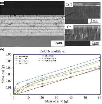
multilayer system by depositing successive layers of overlay coatings [21-23]. Fig. 2.4
resistance of Inconel® 718. While thin physically deposited multilayers are very promising
in improving the wear resistance, the deposition time and the associated cost of these
coatings is very high [17].
Figure 2.4: (a) Multilayer coating of Cr/CrN on an Inconel® 718 substrate.
(b) Erosion resistance of the coating when subjected to bombardment with SiC
particles (adapted from [24]).
2.2.2 Diffusion Coatings
Hard surfaces are commonly made on metal structures through a process that involves
solid-state diffusion of an alloying element into the metal. This technique is relatively easy
to perform and can invoke significant alloy element diffusion to depths up to about
100 µm. Depending upon the alloy element used, significant solid-solution and/or
chemical composition of the material in the diffusion zone ensures a gradient in interatomic
spacing which reduces the inter-atomic mismatch strains within the diffusion zone. This
reduces the chance for adhesive failure of the material within the hardened diffusion zone
from the substrate and results in a hardened layer that is more resistant to abrasive wear
[17].
Numerous diffusion coating techniques have been developed over the last century but the
oldest, and still the most commonly used, is the pack or solid cementation process. In this
process the diffusing agent is in form of a powder composed of three components; i) the
metal powder to be diffused into the substrate, ii) a halide compound that facilitates the
diffusion process, and iii) a filler material that controls the kinetics of the diffusion process.
The material to be surface hardened is embedded in the agent powder and is heated up to
the diffusion temperature. At this temperature, the halogen-carrying compound
decomposes, and the halogen part forms a metal halide gas with the metal that is to be
diffused into the substrate. When this gas adsorbs on the surface of the substrate it releases
the metal atoms and the halogen part then returns to its original activator composition to
repeat its task of transferring metal atoms [7]. Fig. 2.5 summarizes this mechanism.
This technique for making diffusion coatings is frequently applied to create carbon,
nitrogen, and/or boron diffusion hardened layers on steel alloys [25]. Nonetheless,
carburizing and nitriding are not ideal for nickel alloys because of the very limited
solubility of carbon and nitrogen in nickel [15, 25]. Boron, on the other hand, forms
extensive strongly bonded intermetallic compounds with nickel and this results in
significantly improved diffusion coatings. The life of boride diffusion layers is more than
twice that of carbide or nitride diffusion layers on Ni-based alloys subjected to intense
abrasive wear loadings [25].
2.2.2.1 Boride Diffusion Layers on Nickel Bearing Alloys
Solid or pack boronizing of nickel bearing alloys is very attractive because of the simplicity
of the technique, the unsophisticated equipment required, and its cost-effectiveness
[26-27]. The boriding powder, consisting of a boriding agent, halogen activator and filler,
is packed around a workpiece in a steel container and is heated up to between 700 and
1100 oC in a furnace with controlled atmosphere (nitrogen, helium or argon) for
3 to 16 hours in order to form a smooth boride layer through diffusion [2, 26, 28-29].
2.2.2.2 Boriding Agents
Various types of powders, from amorphous pure boron powder to proprietary boron-rich
powders have been used to perform boronizing of nickel-based alloys (Table 2.2). BorTec
GmbH & Co .KG is a German supplier for various grades of boriding powders with brand
name Ekabor®. Some versions of these products are Ekabor® II, Ekabor® III [28] and
Ekabor® Ni [30]. Ekabor® II contains 5% B4C, 5% KBF4 and 90% SiC. KBF4 is the
activator and silicon carbide (SiC) serves as the diluent. Formation of the boride layer is
based on the mechanism that was already described in Fig. 2.5 that is BF3 gas formation
which transfers boron atoms on the surface of the substrate to form boride islands [7, 31].
Furthermore, diluent SiC enforces some more reactions to the system by making silicide
compounds that assist controlling the rate of layer formation [6, 32]. In other words, when
temperature exceeds 600 oC, SiC particles oxidize to form a barrier SiO2 on the surface.
then, KBF4 decomposes to BF3. Subsequently, reaction between BF3 and SiO2 result in
enable further oxidation of SiC. SiF4 tends to react with atoms of nickel and those of other
elements to form Ni2Si, Fe2Si, Ni5Si etc. (Eq.2.2 and 2.3) [6]. The silicide compounds slow
the process of boride diffusion and thus limit the thickness of boride layer [6, 33].
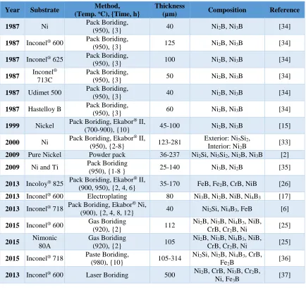
Table 2.2: Chronological sequence of studies on boronizing of nickel-based alloys.
Year Substrate Method, (Temp. oC), {Time, h}
Thickness
(µm) Composition Reference 1987 Ni Pack Boriding,
(950), {3} 40 Ni2B, Ni3B [34]
1987 Inconel® 600 Pack Boriding,
(950), {3} 125 Ni2B, Ni3B [34]
1987 Inconel® 625 Pack Boriding,
(950), {3} 100 Ni2B, Ni3B [34]
1987 Inconel ®
713C
Pack Boriding,
(950), {3} 50 Ni2B, Ni3B [34]
1987 Udimet 500 Pack Boriding,
(950), {3} 40 Ni2B, Ni3B [34]
1987 Hastelloy B Pack Boriding,
(950), {3} 60 Ni2B, Ni3B [34]
1999 Nickel Pack Boriding, Ekabor
® II,
(700-900), {10} 45-100 Ni2B, Ni3B [15]
2000 Ni Pack Boriding, Ekabor
® II,
(950), {2-8} 123-281
Exterior: Ni5Si2,
Interior: Ni2B [33] 2009 Pure Nickel Powder pack 36-237 Ni2Si, Ni5Si2, Ni2B, Ni3B [2] 2009 Ni and Ti Pack Boriding
(950), {1-8 } 25-140 Ni3B, Ni2B [35]
2013 Incoloy® 825 Pack Boriding, Ekabor® II,
(900, 950), {2, 4, 6} 35-170 FeB, Fe2B, CrB, NiB [26]
2013 Inconel® 600 Electroplating 80 Ni
3B, Ni2B, NiB, Ni4B3 [17] 2013 Inconel® 718 Pack Boriding, Ekabor® Ni,
(900), {2, 4, 8, 12} 40 Ni2Si, Ni4B3, FeB [6]
2015 Inconel® 600 Gas Boriding
(920), {2} 112
Ni2B, Ni3B, Ni4B3, NiB,
CrB, Cr2B, Ni
[25]
2015 Nimonic
80A
Gas Boriding
(920), {2} 105
Ni2B, Ni3B, Ni4B3, NiB,
CrB, Cr2B, Ni
[25]
2015 Inconel® 718 Paste Boriding,
(980), {10} 105-314
Ni2Si, Ni2B, Ni4B3, CrB,
Fe2B
[36]
2013 Inconel® 600 Laser Boriding 500 Ni2B, CrB, Ni3B, Cr2B,
Ni, Fe3B [37]
3SiO2 + 4BF3 → 3SiF4 + 2B2O3 (2.1)
2SiF4 + 5Ni → Ni5Si2 + 4F2 (2.2)
The nickel silicide, Ni5Si2, on the surface has equiaxed granular morphology and Ni2B has
needle-shaped structure. In one study the resulted coating consisted in 281 µm silicide layer
on top and only 10 µm boride layer [33].
Due to considerable amount of silicon, Ekabor® II ends up with an inner boride layer and
an outer porous silicide layer [2, 37]. While a multi-layer coating has some protective
benefits at high temperatures the outer silicide layer is softer than the boride layer and is
thus not desirable. Besides, the silicide layer has a very low thermal expansion coefficient
compared to the boride layer and thus, if the silicide layer is thick, large residual strain
accumulates in the layer leading to crack formation [6-7].
Recently the BorTec GmbH & Co .KG has introduced a new nickel boriding powder
formulation, Ekabor® Ni that has less silicon compound agent and thus limits the extent to
which a nickel silicide layer forms during boriding [2, 15]. It is this boriding agent that will
be used in the studies of this thesis.
2.2.2.3 Structure and Composition of a Boride Coating on a Nickel Alloy
The nickel-boron binary phase diagram is shown in Fig. 2.6 and indicates the presence of
various NixBy intermetallic phases [38]. The pack boronizing process naturally results in
the development of a boron concentration gradient within the near surface of the boronized
nickel alloy [39]. Therefore, NiB, Ni4B3, and Ni2B, precipitates may exist in different
regions of the boron diffusion zone. The final composition of the boride layer (e.g. NiB,
Ni2B, Ni3B, NiB2, etc.) depends on the thermodynamic activity of each of the compounds
[16].Table 2.3 shows crystallographic data of the nickel boride phases that are present in
a borided nickel-chromium alloy system similar to Inconel® 718 [17].
The morphology of this multiphase boride layer affects many properties of the layer since
the hardness of each phase is different (HNiB= 1800 Knoop, HNi2B =1400 Knoop) [11].
Besides, siliciding causes the layers close to the surface be enriched of silicon with Ni2Si
crystals which has low hardness [36]. The resulting coating consists of a top silicate layer
intermetallic compounds and diffusion zone consisting of grain boundary diffusion zone
(Fig. 2.7) [6, 18, 34].
Figure 2.6: Nickel-Boron binary phase diagram (adapted from [38]).
Table 2.3:Crystallographic parameters and coefficient of expansion of nickel and
chromium borides [17, 25].
Phase Ni
#70-1849
Ni2B
#82-1697
Ni3B
#89-3822
Ni4B3
#73-1793
NiB
#74-1207
Cr2B
#89-4876
CrB
#89-3587
Crystal
Structure Cubic Tetragonal Orthorhombic Orthorhombic Orthorhombic Tetragonal Orthorhombic Space Group Fe3̅m 14/mcm Pbnm Pnma Cmcm 14/mcm Cmcm
Volume (Å3) 43.80 105.82 151.38 234.10 64.16 - -
Lattice Parameters
(Å)
a = 3.525 b = 3.525 c = 3.525
a = 4.992 b = 4.992 c = 4.2465
a = 4.389 b = 5.211 c = 6.619
a = 11.954 b = 2.9815 c = 6.5684
a = 2.925 b = 7.396 c = 2.966
a = 5.1850 b = 5.1850 c = 4.3160
a = 2.9782 b = 7.8790 c = 2.9346
Density
(g/cm3) 8.90 8.05 8.20 7.58 7.20 - 6.17
2θ (I100, %)
(Deg.) 44.481 45.886 46.004 43.676 45.195 45.195 45.195 d (I100, %) (Å) 2.0352 1.9761 1.9713 2.0708 2.0047 2.0047 2.0047
Coefficient of Expansion
(oC-1)
11.4 × 10⁻⁶ 7.64 × 10⁻⁶ 7.9 × 10⁻⁶ - - - -
Figure 2.7: Coating structure of a borided surface (adapted from [34]).
2.2.2.4 Effect of Alloying Elements on Boride Hardness and Thickness
F. Matsuda et al. carried out an investigation on the effect of alloying elements on the
hardness and thickness of boride coatings. Binary alloys of nickel with either Ti, Zr, Hf,
V, Nb, Ta, Cr, Mo, Mn, Fe, Co, Al or Si were prepared and then boronized at 950 oC for
three hours. The average hardness and thickness of the resulting boride layer is shown as a
function of alloy content in Fig. 2.8 [34].
Figure 2.8: Effect of alloying element on the hardness (a), and coating thickness (b)
Most of alloying elements increase the hardness of the coating layer by forming various
types of boride precipitates which are actually harder than the nickel boride phase.
Therefore, up to 18% chromium, which is about the same amount as Inconel® 718,
significantly increases the hardness of the boride layer. In contrast, Makuch et al. reported
that alloying elements, such as chromium, often decrease the thickness of the boride layer
by increasing the activation energy for solid-state diffusion of boron in nickel [25]. 2.9 Based on these results Matsuda et al. deduced that the most effective alloying elements for
improved boride layer hardness and thickness for nickel-based alloys are Ti, Nb (<5 wt.%),
V, Cr (>10 wt.%) and Mo [34]. They proposed the following empirical equation to predict
the Vickers Hardness (VH) of the boron layer as a function of the chemical composition of
the borided alloy as:
HValloy = 220 × Hf (wt.%) + 170 × Zr + 95 × Ti + 54 × (2.4)
Ta + 46 × Nb + 44 × Si + 38 × V + 25 × Mo +
13 × Co + 5 × Mn + XCr + YFe + 800
where,
XCr: 47 × Cr (Cr ≤ 10%), 14 × Cr + 330 (Cr >10%) (2.5)
YFe: 13 × Fe (Fe ≤ 10%), 130 (Fe >10%) (2.6)
While the form of this equation has great potential usefulness for those considering to use
a pack boriding process to surface harden a nickel-based alloy, its empirical nature results
in it being quite inaccurate. The measured Vickers hardness of a selection of commercial
alloys (Inconel® 600, Inconel® 625, Inconel® 713C, Udimet 400, and Hastelloy B) were
about 250 to 610 HV less than that predicted by Eq. 2.4 [34].
2.2.2.5 Effect of Time and Temperature on the Boride Layer Thickness
Generally speaking, the thickness of coating increases with time and temperature [40].
temperature and, for a given temperature, the approximately linear dependence of layer
thickness upon boriding time [2, 15].
Figure 2.9:Relationship between (a) boriding temperature, (b) boriding time and
boride layer thickness for a nickel-based alloy (adapted from [2, 15]).
An important observation associated with the study depicted in Fig. 2.9 is that when the
boriding process was conducted at a very high temperatures, “flaking of treated layer occurred and thick boride layer was not obtained” [15].
2.2.2.6 Wear Properties
As was discussed in section 2.2.2.4, boride compounds significantly improve the hardness
of nickel bearing alloys. The wear resistance of nickel-bearing alloys is also improved to
the point where borided nickel-based alloys have wear resistance similar to sintered
carbides [25]. The amount of metal loss due to wear is about 100 times less for borided
samples than for untreated ones [15]. The boride layer can also significantly decrease the
coefficient of sliding friction [18]. As a case in point, the coefficient of sliding friction (µ)
of untreated Inconel® 718 is about 0.8 while that of borided Inconel® 718 is 0.4 to 0.7 [15,
36]. Higher boronizing temperature causes a harder boride layer with lower coefficient of
3 EXPERIMENTAL PROCEDURE
In this investigation, the effect of pack boronizing and thermal aging on the indentation
hardness and the wear resistance of the nickel-based Inconel® 718 alloy is studied. Samples
of this alloy were obtained from VDM METALS Ltd (Nevada, US). The chemical
composition of the alloy is shown in Table 3.1 and is within the range defined by
SAE AMS 5663M and ASTM A1014-03 [3-4]. The as-received alloy was in the solution
annealed condition (982 oC for 1 hour followed by water quenching).
Table 3.1:Chemical composition of Inconel® 718 in comparison with the standard
composition range for this alloy [3].
Element
(wt. %) Ni Cr Nb Mo Ti Co Al Mn Si Cu C
Min. 50 17.0 4.75 2.80 0.65 0 0.20 0 0 0 0 Max. 55 21.0 5.50 3.30 1.15 1 0.80 0.35 0.35 0.3 0.08
Sample 53.96 18.34 5.33 3.03 0.96 0.20 0.61 0.08 0.06 0.05 0.030
Element
(wt. %) Ta Ca S P B Mg Pb Se Bi Fe
Min. 0 - 0 0 0 - 0 0 0
Bal. Max. 0.05 - 0.015 0.015 0.006 - 0.0005 0.0003 0.00003
Sample 0.01 <0.010 0.001 0.008 0.004 0.0030 0.0001 >0.0001 0.00001 17.22
Two sets of samples were prepared from the Inconel® 718 material (Fig. 3.1): i) The first
set were cylindrical buttons of 10 mm diameter and 6 mm height. These samples were used
for microstructural studies and hardness measurements. ii) The second set was cylindrical
discs and pins used for wear evaluations. The cylindrical discs were of 6.4 mm thickness
with 6.4 and 25.4 mm inner and outer diameter respectively. The pins were of 6.4 mm
diameter and 25.4 mm length. Two samples were made of each set for each thermal
condition described in Section 3.1. Both flat surfaces of the samples were then prepared by
mechanical grinding with successively finer, from 800 to 2000 grit, SiC abrasive paper
Figure 3.1: Inconel® 718 samples (a) button sample; (b) disc and pin wear test
sample; (c) disc dimensions; (d) pin dimensions.
3.1 Thermal Treatments
The polished Inconel® 718 samples were then subjected to two thermal processes i) age
hardening (aging) and/or ii) pack boronizing. The order of the processes was changed to
investigate the effect of the combined processes on the overall hardness and wear resistance
of the alloy. The following five conditions were considered:
AB: In this condition the samples were first aged and then boronized.
BA: In this condition the samples were first boronized and then aged.
SAB: In this condition the samples were simultaneously aged and boronized.
JB: In this condition the samples were just boronized and not aged.
JA: In this condition the samples were just aged and not boronized.
For simplicity, these conditions will be referred to by their abbreviations. The Aging and
Boronizing thermal treatments are described below.
3.1.1 Aging Treatment
Aging thermal treatment was performed according to ASTM A1014-03 and
ASTM B 637-12 [3, 9]. The samples were heated in vacuum (6.6 × 10⁻² torr) up to 718 °C
for 8 hours, followed by slow cooling (100 °C/hr) to 620 °C, held at this temperature for
another 8 hours, and cooled in air to room temperature. The aging thermal
treatments were performed in an Ipsen vacuum induction furnace located at
Figure 3.2: Vacuum furnace employed for aging treatment.
3.1.2 Boriding Treatment
Boronizing was performed in a Thermo-Thermolyne FD 1500 Industrial Furnace (Fig. 3.3)
operating with a flowing Ar gas atmosphere to prevent oxidation of the samples. This
furnace is located at Surface Heat Treat and Coating Co. in Hamilton, Ontario. The
boriding agent used in this project was Ekabor® Ni powder purchased from BorTec Co. of
Germany. The exact chemical composition of the Ekabor® Ni powder is proprietary and,
hence not available, however previous researchers have analysed its composition with
X-ray diffraction analysis and have reported that it contains little or no SiC but contains
Ca6B and traces of KBF4 activating powders [2]. The Inconel® 718 samples were placed in
small steel containers which were then packed with the Ekabor® Ni powder.
For the AB, BA, and JB samples, the packed containers were heated to the boriding
temperature of 800 oC and held for 5 hours. For the SAB samples the boriding was done in
same furnace but with a thermal cycle that would promote concurrent age hardening of the
Inconel® 718 samples (718 °C for 8 hours, cooling down with rate 100 °C/hr and holding
Figure 3.3:Thermo-Thermolyne FD 1500 industrial furnace.
3.2 Evaluations and Equipment
After the aging and/or boronizing thermal treatments, the surface morphology/roughness,
microstructure, indentation hardness, and wear resistance of the Inconel® 718 samples were
evaluated using the equipment and methodologies described below.
3.2.1 Surface Morphology and Roughness Measurements.
The surface morphology of the aged and borided samples was studied by optical and
scanning electron microscopy (SEM). The optical microscope used was a Nikon Eclipse
L150 equipped with Nikon Digital Eclipse DXM1200 camera (Fig. 3.5 (a)) while the SEM
was a JEOL JXA-8530F field-emission analytical scanning electron microscope equipped
with secondary- and back scattered-electron detectors and a wavelength dispersive (WDS)
Figure 3.4: Temperature-Time histories of samples subjected to the AB, BA, SAB,
Figure 3.5: (a)Nikon Eclipse L150 optic microscope; (b) SEM microscope
(JEOL JXA 8530F).
The surface roughness of the samples was measured with a Micro Materials Nano Test
indention machine (Fig. 3.6 (a)). This machine consists of a ceramic pendulum on top of
which an electric coil is mounted (Fig. 3.6 (b)). Passage of an electric current through the
coil induces a magnetic field causing the pendulum to be attracted to the magnet. As a
result, the pendulum swings around the pivot, located at its midpoint, causing the sharp
conical diamond indenter, attached to the lower side of the pendulum, to swing toward and
lightly contact the surface of the sample. By maintaining a fixed electrical current to the
coil, a small constant indentation force is applied to the sample. A parallel plate capacitor,
located between the bottom of the pendulum and the fixed base of the instrument, is used
to measure, with high precision, the change in position of the indenter as the sample is
moved by computer-controlled micrometers, on an Y-Z plane perpendicular to the indenter.
The surface roughness of the samples of this study were measured, with this instrument,
using a conical indenter with a 5 µm diameter tip under the application of a small 0.1 mN
indentation load. The samples were moved along the Y- and Z-axes (The indentation
direction was along the orthogonal X-axis) a distance of 200 ± 5 µm while the displacement
of the indenter, indicating the surface roughness, was continuously recorded. Five parallel
horizontal (Y-axis) and five parallel vertical (Z-axis) scans, each spaced 20 µm apart, were
performed on samples from each of the five thermal conditions. An example of a typical
surface roughness measurement is depicted in Fig. 3.7 (a) and (b). The straight black lines
show the path of scanning while the blue lines illustrate the X-axis height deviation of the
Figure 3.6: (a)The Micro Materials Nano Test Indentation testing machine; (b) load
applying and displacement measurement system (adapted from [41]).
Figure 3.7: (a) Roughness condition of sample AB and (b) typical surface roughness
The acquired X-axis height data were used to calculate the average root mean square of
asperity height (Rrms) characteristic of the surface roughness of each sample as
Rrms = √ 1
𝑛∑ 𝑥
2 𝑛
𝑖=1 (3.1)
where x is vertical distance from the mean of the surface at the ith measurement point and
n is the total number of measurement points in the scan.
3.2.2 Microstructural Phase Analyses
The microstructural phases present in the surface region of the aged and/or borided
Inconel® 718 samples were analyzed by X-ray diffraction using a Bruker D8 Advance
diffractometer (Fig. 3.8). A Cu Kα X-ray source (λ = 15.406 Å) was directed on the surface
of the sample and scanned over a range of angles θ relative to the surface normal direction
from 2θ = 10 to 90 degrees. The X-ray diffraction signal was obtained as a function of θ
and the angular position of the Bragg reflection peaks was used to identify the crystal
phases present in the material. This identification was done using the X'Pert HighScore
software manufactured by PANalytical B.V.
3.2.3 Further Microstructural Characterization
Several samples from each thermal condition (AB, BA, SAB, JA, and JB) were
electroplated with a pure copper layer on the borided surface to protect the surface from
rounding during subsequent grinding and polishing operations. The electroplating was
done in an aqueous copper sulfate (CuSO4) solution electrolyte. A pure copper plate was
used as the anode and the sample to be protected was the cathode. A current density of
4 A/dm2 was used for 24 hours to deposit a coating layer of more than 100 µm thickness
onto the sample surface.
The copper plated samples were then sectioned, perpendicular to the borided surface, with
a Buehler IsoMet® low speed diamond saw. The sectioned samples were then mounted in
35 mm diameter disks of fast cure epoxy. The cut surface, perpendicular to the borided
800 to 4000 grit. The ground surfaces were then polished with a
Buehler Inc. Mastermet 2 colloidal silica, 20 nm diameter, aqueous suspension.
To reveal and compare grain size and shape in the regions near the borided surface the
sectioned Inconel® 718 samples were etched with Marble’s reagent (10 ml nitric acid
(HNO3), 10 ml acetic acid (CH3COOH), 15 ml hydrochloric acid (HCl) and 5 drops
glycerine) according to the procedure described in ASTM E 407 [42]. Etching was done
by immersion of the sample in the etchant for between 5 to 7 seconds. This process revealed
the grain structure clearly and allowed the thickness of the borided layer as well as the
grain size to be measured using the established procedure described in ASTM E 112-13
[43].
3.2.4 Indentation Hardness Tests
3.2.4.1 Nanoindentation Hardness Measurements
In order to understand the local variation in hardness resulting from surface coating or
hardening operations it is necessary to perform nano- rather than micro-indention hardness
tests. In this study we used a Micro Materials Nano Test indentation machine (Fig. 3.6) to
perform these nanoindentation hardness measurements. The tests were performed using a
three-sided pyramidal diamond indenter with 50 nm tip radius.
For these tests the indentation force (F) was applied at a constant loading rate of 0.1 mN/s
to a maximum indentation depth of hmax = 300 nm. The nanoindentation tests were
performed on the sectioned Inconel® 718 samples (Section 3.2.2). Multiple
nanoindentations were performed on the plane along a line that began within the bulk
sample, over 25 µm away from the borided surface and extended to, and across the borided
layer by every 1 μm steps. The nanoindentations were spaced about 30 μm apart along the
line to avoid the interaction of one on another (Fig. 3.9). Each indentation test was repeated
up to 9 times. The nano indentation hardness was determined from the F versus h data (Fig.
3.10) obtained from each indentation test using established methods [44-45].
Figure 3.9: Optical image of a typical line of indentations extending
Figure 3.10: Loading-unloading F - h diagram obtained from a typical nano
indentation test (adapted from [44, 45]).
The projected area (Ap) of the indentation is related to the plastic indentation depth (hp),
as:
Ap = 24.5 ℎ𝑝2 [mm2] (3.2)
This equation is valid when the tip of indenter is ideally sharp. However, the original
Berkovich indenter has a tip with 50 nm in radius while the indenter becomes blunter
during service. To avoid error in hardness measurements, “diamond area function
calibration’’ was periodically performed. It is calculating the hardness of a standard sample
(fused silica) with known hardness (9-10 GPa) at various indentation depths. From these
data the projected contact area (Ap) can be determined at each indentation depth (hp). A
high order polynomial function is then fitted to the data to express Ap(hp):
This polynomial contact area function is then used to calculate the indentation hardness of
the test samples as:
𝐻 = 𝐹
𝐴𝑝(ℎ𝑝) (3.4)
3.2.4.2 Microindentation Hardness Measurements
Vickers microindentation hardness measurements were performed on samples from each
thermal condition (AB, BA, SAB, JA, and JB) to assess the hardness of i) the boride
coatings, ii) the transition region below the borided layer, and iii) the bulk material. The
microindentation tests impose a relatively “large” indentation, of several tens of
micrometers dimension, into the material and thus the hardness value obtained from these
tests represents the average hardness of the material. The Vickers microhardness number
(VHN) is an industrial standard for characterizing the yield strength of common
engineering metals since VHN ≈ 3σyield [46]. In this study microindentation hardness tests
were performed, according to established procedure as described in ASTM E 384 [47],
with a Buehler Micromet II Vickers microhardness tester (Fig. 3.11).
For each sample, 5 to 7 indentations were made in each of the three regions described above
at indentation forces of F = 0.01, 0.025 and 0.05 kgf. The diagonal length (d) of the
resulting diamond shaped indentations was measured optically and the Vickers indentation
hardness number was calculated as:
HV = 𝐹
𝐴
≈
1.8544𝐹
𝑑2 [kgf/mm
2] (3.5)
3.2.5 Wear Behavior
A wear machine was developed for this project based on the published standards for
pin-on-disc wear testing, ASTM G 99 (Fig. 3.12 (a)). In this test, two specimens of the same
material become in contact, a disc and a pin. The disc is fixed at the center of a horizontally
aligned revolving wheel while the pin is perpendicularly in contact at a distance from the
central point of the disc. Therefore, a sliding path forms through rotation of the disc. A
suspending weight is applied over the pin to intensify the wear condition (Fig. 3.12 (b)).
Figure 3.12: (a) Developed pin on disc wear test machine; (b) Principles of pin on
The machine is capable of applying a load up to 160 N to an Inconel® 718 pin of 6.4 mm
diameter. The loaded pin is then placed in contact, 8 mm from the central axis, of a 25.4
mm diameter flat disc made of the same material. Pin-disc sets from each Inconel® 718
sample conditions (AB, BA, SAB and JA) were constructed and tested with this apparatus.
Before each test, the pin and disc components were degreased in acetone and isopropanol
and then weighed with a high precision laboratory scale (± 0.0001 g). Wear tests were
performed in the dry, nonlubricated condition under pin-disc contact pressures of 2.5, 3.3,
4.0 and 4.7 MPa. Each wear test was performed to a sliding distance of 1000 m. Each test
was intermittently stopped at 100 m sliding distance increments and the pin and disc were
ultrasonically cleaned in acetone and isopropanol to remove debris and wear products and
then reweighed. The accumulated weight loss of the samples was recorded as a function of
contact pressure and sliding distance. At the end of the wear test the wear tracks on the
4 RESULTS
In this study microstructural analyses, indentation hardness tests, and sliding wear tests
were performed on borided and/or age hardened Inconel® 718 alloy samples to determine
the most effective way to apply a nickel boride hard surface while still retaining the high
mechanical hardness of the age hardened Inconel® 718 alloy. In this chapter, we present
the results of the analyses on the samples made under the five conditions:
AB: In this condition the samples were first aged and then boronized.
BA: In this condition the samples were first boronized and then aged.
SAB: In this condition the samples were simultaneously aged and boronized.
JB: In this condition the samples were just boronized and not aged.
JA: In this condition the samples were just aged and not boronized.
4.1 Microstructural Analyses
4.1.1 Surface Roughness
The data of the typical roughness profiles is shown in Table 4.1. The root mean square of
asperities (Rrms) was calculated using Eq. 3.1. The polished surface of the starting solution
annealed (as received (AR)) Inconel® 718 sample has the lowest RMS surface roughness
(22 µm). The just aging (JA) process increases the roughness slightly (49 µm) however the
boriding process (AB, BA, SAB, or JB) results in substantially increased surface roughness
(388 to 857 µm).
Table 4.1: Root mean square of surface roughness (Rrms) of the Inconel® 718
samples subjected to various aging/boriding conditions.
Sample AR JA AB SAB JB BA
Root Mean Square of Roughness (Rrms) (µm) 22 49 675 388 530 857
Fig. 4.1 shows optical and scanning electron micrographs of the just aged (JA)
Inconel® 718 samples. In contrast, Fig. 4.2, 4.3 and 4.4 depict the rougher surfaces of the
conditions, a relatively uniform boride layer was created with only small regions of
imperfections as shown by the un-sintered particles labelled in Fig. 4.3. The unsintered or
unreacted crystalline structures of Ekabor® Ni particles are obvious in JB, AB and SAB
(Fig. 4.3), but not in BA.
4.1.2 Structure and Thickness of the Boride Layers
Fig. 4.5 shows optical images of polished sections perpendicular to the borided surface of
the Inconel® 718 samples. The boride layer is of generally uniform thickness around the
sample for all conditions. The etched surface of the selected sections in Fig. 4.5 is shown
in Fig. 4.6. The chemical etching process revealed that the boride layer consists of two
zones: i) the Dispersed Zone (DZ) where the nickel boride is present as a continuous phase
and ii) the Grain Boundary Zone (GBZ) where significant diffusion of boron, and hence
precipitation of nickel boride, occurs only along pre-existing grain boundaries. These two
zones are labelled in Fig. 4.6. The thickness of the DZs, GBZs, and overall boride layer are
given in Table 4.2 for each boriding condition tested.
A significant observation that can be made from Fig. 4.5 is the tendency of the JB, AB, and
SAB samples to contain large cracks running through the DZ region of the boride layer.
No crack was observed in the boride layer of the BA samples.
Figure 4.1:Surface condition in just aged (JA) condition. (a) 100X, (b) 500X and
Figure 4.2: Surface appearance after coating process at 100X; (a) JB,
(b) AB, (c) SAB, (d) BA.
Figure 4.3: Surface appearance after coating process at 500X. (a) JB,
Figure 4.4: SEM micrographs of coating surface at 1000X; (a) JB,
(b) AB, (c) SAB, (d) BA.
4.1.3 Chemical Composition of the Coating
As a precursor to our assessment of the chemical composition and phase identification
within the various boride layers, X-ray diffraction analysis was performed on the starting
Ekabor® Ni powder that was used as the pack in all the boriding treatments performed in
this study. While the exact chemical composition of the Ekabor® Ni powder is classified,
previous researchers have analysed its composition with X-ray diffraction analysis and
have reported that it contains little or no SiC but contains Ca6B and traces of KBF4 powders
[2]. Fig. 4.7 shows the indexed X-ray diffraction peaks obtained from a backscattered
analysis of the Ekabor® Ni powder. The powder is composed of B
4C, Si6B, CaF2, and
Figure 4.5: Unetched optical micrographs of the uniform boride layer
on samples from the (a) JB, (b) AB, (c) SAB, and (d) BA conditions.
Figure 4.6: Optical micrographs of the chemically etched boride layer
Table 4.2: Average boride coating thickness for different conditions.
Condition
Thickness (µm) JB AB SAB BA Dispersed Zone 29.5 25.6 15 15.1
Grain Boundary Zone 24.5 32.8 9.9 20.3
Overall 54.0 58.4 24.9 35.4
Similar to described mechanism in Fig. 2.5, in this Ekabor® Ni powder mixture, the B4C
and Si6B act as the boron carrying agent, the CaF2 acts as an activator to encourage the
decomposition of the carrying agents and the precipitation of nickel- or iron- borides, while
the Ni2O3 is a filler powder. The presence of silicon in the Ekabor® Ni powder results in
the possibility of NixSiy precipitation during the subsequent boriding process.
Figure 4.7: Indexed X-ray diffraction profile of the Ekabor® Ni
boriding powder.
Indexed X-ray diffraction peaks of the borided layers (JB, AB, SAB, and BA) are shown
in Fig. 4.8. These profiles indicate that a variety of nickel-/iron-borides,
chromium-/molybdenum-borides, nickel-silicides, and nickel-oxides are present in the
borided layer of the samples and the phases present are dependent upon the boriding/aging
treatment.
Fig. 4.9 shows SEM WDS X-ray boron and silicon composition maps of the polished
planes perpendicular to the various borided surfaces. A notable finding shown in these
figures is that nickel silicides appear on the top surface of the boride layer under certain
36 Figure 4.8: X-ray diffraction profiles of borided surface of samples in various boride conditions: (a) JB; (b) AB; (c) SAB;
37 Figure 4.9: SEM WDS X-ray composition maps of aged and borided Inconel® 718 samples reveal the presence of boron and
Fig. 4.10 shows more details of chemical analysis in the boride layer of the AB condition.
These observations reveal that the boride layer is actually composed of two sections; i) a
thin, 2-4 µm thick, nickel silicide layer at the top (Compound Zone) and ii) a thicker
underlying nickel-/iron-/chromium-boride layer (Dispersed Zone). X-ray point analyses
indicate that the amount of nickel in the upper region (i) is 80% while it is about 40% in
the lower region (ii), and about 52% in substrate Inconel® 718.
Figure 4.10: SEM BSE image (a), and WDS map of AB sample for (b) Ni,
(c) Cr, (d) Si, (e) Fe.
Fig. 4.9 indicates that the thickness of the nickel silicide region is very dependent upon the
that all the samples were produced from the same Ekabor® Ni boride powder. This disparity
is discussed inChapter 5.
4.2 Hardness of the Coating
4.2.1 Nanoindentation Hardness
Table 4.3 summarizes measured nanoindentation hardness while Fig. 4.11 depicts the
indentation track across the coating layer and the corresponding typical measured hardness
profile of the various borided/aged Inconel® 718 samples. The nanoindentation tests were
performed in parts of the coating that contained cracks in order to assess whether the
cracking corresponded to regions in the coating that displayed very high, or very low, local
hardness.
Table 4.3: Nanoindentation hardness test results of the various borided/aged
Inconel® 718 samples.
Condition Maximum Hardness (GPa) {HV} Thickness (µm) Average hardened layer (µm) Total thickness of Hardness at Crack (GPa) {HV} Bulk (GPa) {HV} Hardness of the
JA - - - - 8.9 {907.5}
JB 31.2 {3181} 25 30 21.4 {2182} 5.7 {581}
AB 30.5 {3110} 29 32 7.2 {734} 8.2 {836}
SAB 27.2 {2774} 13 16 12.9 {1315} 9.4 {958}
BA 25.3 {2580} 15 20 - 7.8 {795}
The Just Aged (JA) sample displayed a uniform hardness with little hardness variations
from the edge to the bulk of the sample (average hardness 8.9 GPa). The borided samples,
on the other hand, displayed significantly increased hardness in the borided region. The
hardness within the borided region of these samples was between 20 to 31 GPa.
Table 4.3 indicates that the Just Borided (JB) samples had the lowest bulk hardness
(5.8 GPa) while the aged samples (JA, AB, BA and SAB) displayed the highest bulk
hardness (7.5 to 9.4 GPa). The variability in the bulk hardness of the samples that were
both borided and aged reflects the effect of the boriding thermal process on the
microstructure created during the aging process. This will be discussed in more detail in
40 Figure 4.11: Nano hardness profile of samples across the borided layer and in the bulk of the Inconel® 718 alloy. The error
4.2.2 Microindentation Hardness
The nanoindentation hardness data, presented above, provide data on the fluctuations of
hardness through the borided layer. The microindentation,Vickers, hardness data give a
collective and complementary vision of the overall hardness of the boride layer and the
bulk Inconel® 718 substrate alloy. Table 4.4 and Fig. 4.12 illustrate the Vickers hardness
of the borided layer and substrate. The results confirm the findings of the nanoindentation
hardness. Fig. 4.13shows a typical Vickers hardness test that was done on the SAB sample.
The size of the indentations illustrates the increased hardness of the coating compared to
the substrate.
Table 4.4: Vickers hardness of aged and/or borided coatings.
Hardness (VHN) Condition
Coating Interface Bulk Coating vs Substrate (%)
JA - - 376 -
JB 1590.3 443.2 354.8 348
AB 1558.8 557.1 364 328.2
SAB 1526.5 449.1 381.4 300.2
BA 1169.3 478.3 373.2 213.3
Figure 4.12: Hardness of the coating, interface and substrate of samples from the


![Figure 2.5: General mechanism of pack cementation (adapted from [7]).](https://thumb-us.123doks.com/thumbv2/123dok_us/1965030.1259132/20.612.137.522.437.656/figure-general-mechanism-pack-cementation-adapted.webp)
![Table 2.3: Crystallographic parameters and coefficient of expansion of nickel and chromium borides [17, 25]](https://thumb-us.123doks.com/thumbv2/123dok_us/1965030.1259132/24.612.146.505.127.427/table-crystallographic-parameters-coefficient-expansion-nickel-chromium-borides.webp)
![Figure 2.7: Coating structure of a borided surface (adapted from [34]).](https://thumb-us.123doks.com/thumbv2/123dok_us/1965030.1259132/25.612.112.535.424.664/figure-coating-structure-of-borided-surface-adapted-from.webp)


