ISSN (Print) : 2320 – 3765 ISSN (Online): 2278 – 8875
I
nternational
J
ournal of
A
dvanced
R
esearch in
E
lectrical,
E
lectronics and
I
nstrumentation
E
ngineering
(An ISO 3297: 2007 Certified Organization)
Vol. 4, Issue 5, May 2015
Survey on Reduction of Ground Bounce Noise
in Combinational Circuits
Megha Agarwal
Sr. Assistant Professor Dept of ECE, ABES-EC, Ghaziabad, U.P., India
ABSTRACT: One of the effective method to reduce leakage current in logic circuits during sleep mode is Power gating technique. However, conventional power gating technique for minimizing leakage current introduces ground bounce noise during sleep to active mode transition. This Ground Bounce Noise or Power Gating Noise (PGN) which is generated during mode transition from SLEEP to ACTIVE mode is an important challenge in standard MTCMOS circuit. In this paper various Ground Bounce Noise reduction techniques in MTCMOS circuit has been discussed. An intermediate relaxation mode is investigated to gradually dump the charge stored on the virtual lines to the real ground distribution network during the SLEEP to ACTIVE mode transitions. In addition to this a high performance stacking power gating structure is discussed which minimizes the leakage power and provides a way to control the ground bounce noise in transition mode
KEYWORDS:Ground Bounce Noise, Power Gating, mode transition, intermediate mode.
I. INTRODUCTION
Shortening the gate length of a transistor increasesits power consumption due to the increased leakage current between the transistor’s source and drain during standby mode. A tremendous increase in transistor leakage current is the primary disadvantage of technology scaling. There are several different techniques that can be used to deal the leakage current problem from various angles. Multithreshold CMOS (MTCMOS) technology[1], [2], also frequently referred to as power-gating,is a widely used technique for reducing leakage power duringstandby (or sleep) mode.
In this technique a NMOS sleep transistor is connected between the circuit and the ground. During standby mode the sleep transistor is turned off, this in turn disconnect the path between the circuit and the ground and thereby reduces the leakage current significantly.When an MTCMOS circuit make transitions from the SLEEP mode to the ACTIVE mode, a high instantaneous short circuit currents flow through the sleep transistors. Large voltage fluctuations occur on both the real power line (power bouncing noise) and the real ground (ground bouncing noise). Bouncing noise generated in one power-gating domain during a wake-up event is transferred through the shared power and ground distribution networks to the surrounding active circuit blocks. The ground bouncing noise is becoming an increasingly important issue in deeply scaled multi domain MTCMOS circuits.
II. BACKGROUND
ISSN (Print) : 2320 – 3765 ISSN (Online): 2278 – 8875
I
nternational
J
ournal of
A
dvanced
R
esearch in
E
lectrical,
E
lectronics and
I
nstrumentation
E
ngineering
(An ISO 3297: 2007 Certified Organization)
Vol. 4, Issue 5, May 2015
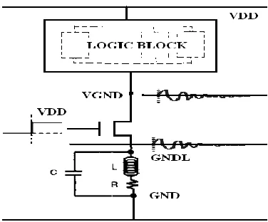
makes the sleep transistor turn ON in saturation. This instantaneous discharge through the sleep transistor which is operating in saturation region creates current surge at sleep/active mode transition, and causes high ground bounce noise [3]-[6].
Figure 1: Ground bounce noise in conventional power gating structure
Besides wasting power and increasing the wake-uptime, these current surges also cause voltage fluctuations in the power/ground network due to the parasitic impedances of the off-chip bonding wires and the on-chip power rails. The power gating noise (PGN) which includes the IR-drop and Ldi/dt during the wake-up process, can induce logic errors, increase the critical path delay of neighboring on-state circuits and affect the power plane integrity in low-power SoCsimplemented in deeply scaled technologies which have narrow noise margins [4], [7]. Detailed studies on PGN in different power-gated MTCMOS combinational and sequential circuits have been recently reported in [7] and [8] respectively. A common response for reducing PGN is to add extra decoupling capacitance which is not very effective because in order to limit Ldi/dt noise to allowable levels, the amount of decoupling capacitance required is very large. During last one decade, various alternatives and improvements of conventional power gating have been proposed.
III. GROUND BOUNCE NOISE REDUCTION TECHNIQUES
Different Ground Bounce Noise reduction techniques for combinational circuits are presented in this section. The Stacking Power gating technique is reviewed in Section III-A. The trimode MTCMOS circuit technique is introduced in Section III-B. The dual-switch MTCMOS circuit technique is presented in Section III-C
A. Stacking Power gating technique
ISSN (Print) : 2320 – 3765 ISSN (Online): 2278 – 8875
I
nternational
J
ournal of
A
dvanced
R
esearch in
E
lectrical,
E
lectronics and
I
nstrumentation
E
ngineering
(An ISO 3297: 2007 Certified Organization)
Vol. 4, Issue 5, May 2015
Figure2. Stacking Power gating technique
In this technique, to reduce the leakage current the stacking effect has been exploited. Both M1 and M2 has been placed as a stack and the stack effect will take place by turning both M1 and M2 sleep transistors OFF. This raises the intermediate node voltage VGND2 to positive values due to small drain current. Positive potential at the intermediate node has four effects:
1) The Vgs1 i.e. Gate to source voltage of M1 becomes negative
2) Negative Vbs1 of M1 i.e. body-to–source potential, causes more body effect
3) Drain-to-source potential (Vds1) of M1 decreases,resulting in less drain induced barrier lowering
4) Drain -to -source potential (Vds2) of M2 is less compared to M1, because most of the voltage drops across the M1 in sleep mode. This significantly reduces the drain induced barrier lowering. The expression for the sub threshold leakage current is
Isub = A𝑒𝑛𝑘𝑇𝑞 (𝑉𝑔𝑠 −𝑉𝑡ℎ0+𝛾𝑉𝑏𝑠 +𝜂𝑉𝑑𝑠 ) (1-𝑒−𝑞𝑉𝑑𝑠𝑘𝑇 ) (1)
Where A= μ0Cox (W/Leff) (kT/q),Vgs, Vds, and Vbs are the gate-to source, the drain-to-source, and the bulk-to-source voltages, respectively. The bulk is connected to ground.
γ
andη
are the body effect and DIBL coefficients respectively. Vth0 is the zero-bias threshold voltage. Cox is the gate-oxidecapacitance. μ0 is the zero-bias mobility, and is the subthreshold swing coefficient.From equation (1) it is observedthat an increase in the body effect (negative Vbs), andreduction in Vds (less DIBL) reduce the sub threshold currentexponentially.
In this technique ground bounce noise thatoccurs during mode transition is reduced by adopting the the following strategy:
ISSN (Print) : 2320 – 3765 ISSN (Online): 2278 – 8875
I
nternational
J
ournal of
A
dvanced
R
esearch in
E
lectrical,
E
lectronics and
I
nstrumentation
E
ngineering
(An ISO 3297: 2007 Certified Organization)
Vol. 4, Issue 5, May 2015
2) By turning ON the M2 transistor in linear region instead ofsaturation region to decrease the current surge.During sleep to active mode transition, transistor M1 isturned ON and transistor M2 is turned ON after a smallduration of time (ΔT). The logic circuit is isolated from theground for a short duration as the transistor M2 is turned OFF.During this duration, the ground bounce noise can be greatlyreduced by controlling the intermediate node voltage VGND2and operating the transistor M2 in triode region.
The intermediate node (VGND2) voltage can be controlledby 1) Inserting proper amount of delay, that is less than the discharging time of the M1 transistor.
2) Proper selection of the capacitance C2.
Figure3. Trimode power-gating structure. High |Vth| sleep transistorsare represented with a thick line in the channel region.
B. Trimode MTCMOS technique
The trimode power-gating structure (proposed in [10]) is presented in this section. An additional intermediate PARK mode is introduced between the SLEEP mode and the ACTIVE mode to lower the ground bouncing noise during transition. A high- | Vth| PMOS transistor (Parker) is connected in parallel with the footer sleep transistor (N1) as shown in Fig. 3.
ISSN (Print) : 2320 – 3765 ISSN (Online): 2278 – 8875
I
nternational
J
ournal of
A
dvanced
R
esearch in
E
lectrical,
E
lectronics and
I
nstrumentation
E
ngineering
(An ISO 3297: 2007 Certified Organization)
Vol. 4, Issue 5, May 2015
are not described in sufficient detail in [10]. Design tradeoffs such as the fluctuations of ground bouncing noise with the duration of the PARK mode, the size of the Parker, and the temperature are not evaluated in [10].
C. Dual-Switch MTCMOS Technique
Another Dual switch MTCMOS technique (proposed in [11]) reviewed in this section. As shown in Fig. 4, a high-Vth nMOS transistor(N2) is connected in parallel with a header sleep transistor (P1) between the real power supply and the virtual power line. Similarly, a high |Vth| pMOS transistor(P2) is connected in parallel with a footer sleep transistor (N1) between the real ground and the virtual ground line. In this technique in between the transition from sleep mode to active mode an intermediate HOLD mode (similar to the PARK mode in [10]) is realized by turning on P2 and N2 while the header and the footer are maintained cut-off. During the SLEEP mode, P1, N1, P2, and N2are turned off to reduce the subthreshold leakage currents. The voltagesof the virtual power and ground lines are approximately equalized. Prior to the switch the circuit to ACTIVE mode, P2 and N2 are activated. As a result the circuit transitions from the SLEEP mode to an intermediate HOLD mode. A differential voltage of VDD- Vth -|Vtp| is produced between the virtual lines. Then to complete the transition process i.e. to switch the circuit from HOLD mode to ACTIVE mode P1and N1 are activated. The virtual power line is charged to ~VDD. The virtual ground line is discharged to ~Vgnd. The groundbouncing noise is reduced by reducing the voltage swings on the virtual lines during the transition from the SLEEP mode to the ACTIVE mode through the HOLD mode, as shown in Fig. 4. Similar to [10], a detailed analysis of the ground-bouncing-noise generation process is not provided in [11]. The effects of the proposed two-step activation scheme and the temperature on theground bouncing noise and the design tradeoffs related to the dual-switch technique are not explored in [11].
Figure4.Dual-switch power-gating structure. High |Vth| sleep transistors are represented with a thick line in the channel region
V. CONCLUSION
ISSN (Print) : 2320 – 3765 ISSN (Online): 2278 – 8875
I
nternational
J
ournal of
A
dvanced
R
esearch in
E
lectrical,
E
lectronics and
I
nstrumentation
E
ngineering
(An ISO 3297: 2007 Certified Organization)
Vol. 4, Issue 5, May 2015
REFRENCES
[1]S. Mutoh, T. Douseki, Y. Matsuya, T. Aoki, S. Shigematsu, and J.Yamda, “1-V power supply high-speed digital circuit technology withmulti-threshold voltage CMOS,” IEEE J. Solid-State Circuits, vol. 30, no. 8, pp. 847–854, Aug. 1995.
[2] S. Shigematsu, S. Mutoh, Y. Matsuya, Y. Tanabe, and J. Yamada, “A 1-V high-speed MTCMOS circuit scheme for power-down application circuits,” IEEE J. Solid-State Circuits, vol. 32, no. 6, pp. 861–869, Jun. 1997.
[3]Y. Chang, S. K. Gupta, and M. A. Breuer, “Analysis of ground bounce in deep sub-micron circuits,” in Proc. 15th IEEE VLSI Test Symp.,,pp. 110– 116, 1997.
[4] S. Kim, S. V. Kosonocky, D. R. Knebel, K. Stawiasz,D. Heidel, and M Immediato, “Understanding and minimizing ground bounce during mode transition of power gating structure,” in Proc. Int. Symp. Low-Power Electron. Des, pp. 22–25, Aug. 2003.
[5] S. Kim, S. V. Kosonocky, D. R. Knebel, K. Stawiasz,D. Heidel, and M. Immediato, "Minimizing inductive noise in system-on-a-chip with multiple power gating structures," in Proceedings of European Solid-State Circuits: pp. 16-18, 2003.
[6] A. Kabbani and A. J. AI-Khalili, "Estimation of ground bounce effects on CMOS circuits," IREE Transactions on Components and Packaging Technology, vol. 22, pp. 316-325, June 1999.
[7] H. Jiao and V. Kursun, “Ground-bouncing-noise-aware combinational MTCMOS circuits,” IEEE Trans. Circuits Syst. I, Reg. Papers, vol. 57, no. 8, pp. 2053–2065, Aug. 2010.
[8] H. Jiao and V. Kursun, “Ground bouncing noise suppression techniques for data preserving sequentialMTCMOS circuits,” IEEE Trans. Very Large Scale Integr. (VLSI) Syst., vol. 19, no. 5, pp. 763–773, May 2011.
[9]Bhanuprakash,R. ; Pattanaik,M. ; Rajput,S.S. ; Mazumdar,K. ,Analysis and reduction of ground bounce noise andleakage current during mode transi tion of stacking power gating logic circuits”,TENCON 2009 - 2009 IEEE Region 10 Conference , pp. 1 - 6 ,2009.
[10] S. Kim, S. V. Kosonocky, D. R. Knebel, K. Stawiasz, and M. C. Papaefthymiou, “A multi-mode power gating structure for low-voltageDeep-submicronCMOS ICs,” IEEE Trans. Circuits Syst. II, Exp. Briefs,vol. 54, no. 7, pp. 586–590, Jul. 2007.