Survey Paper on Different Types of Reversible
Programmable Gate
Reena Mannewar, Prof. Pankaj Kumar Vyas
M. Tech. Scholar, Department of Electronics and Communication, SISTec, Gandhi Nagar, Bhopal, India
Assistant Professor, Department of Electronics and Communication, SISTec, Gandhi Nagar, Bhopal, India
ABSTRACT: Today security in digital computing and communication is of prime importance and therefore, cryptography protocol plays a major role. Reversible logic has emerged as one of the most important approaches and more prominent technology nowadays. Power is the main concern for development and growth of modern VLSI designs. In recent years, the growing market of electronic systems suffers from power dissipation and heat removal problem. If more and more power is dissipated, System becomes overheated which in turn reduces the lifetime of the electronic devices.Reversible logic has also promising application in an online and offline testing of faults. Reversibility circuitry is having its application in following areas: low power consumption, quantum computing, and communication and Nano technology.
KEYWORDS: Reversible Gates, Power Dissipation, Combinational Circuit
I. INTRODUCTION
Most traditional computers lose information in the process of computation. Consider the simple two input Boolean AND gate: Observing an output of 0 does not give enough information to identify the input combination that gave rise to the output. In fact, any one of three different input combinations (00, 01, 10) would force the output of the AND gate to 0. In computing the logical AND of two bits, a traditional AND gate would discard that input information. The only inherently logically reversible traditional primitives include the wire and inverter. The conclusions of Landauer and Bennett show that an energy loss of kTln2 joules in the form of heat unavoidably accompanies each bit of information discarded during computation, and that a completely reversible computer is theoretically possible [1, 2]. Only by performing the computation in a logically reversible manner can energy dissipation fall below kTln2 joules per bit per cycle.
Power crisis is a vital problem in today’s world. In recent years, the growing market of electronic systems suffers from power dissipation and heat removal problem. If more and more power is dissipated, system becomes over heated which reduces the life time of the electronic system. The need of microelectronic circuits with low power dissipation leads to the implementation of reversible logic circuit. Bennett [3] proved that the one-to-one mapping between the inputs and outputs of reversible circuit drastically reduces the power consumption and heat dissipation of a circuit. Today security in digital computing and communications is of prime importance and therefore cryptographic protocols play a major role.
There are four major design parameters of reversible circuits. First is the quantum cost which is the number of basic quantum gates like Controlled NOT, Controlled V+ etc. in the reversible circuit. Second is the quantum depth also called quantum delay [4]. Third is the number of ancillary inputs or ancilla inputs which are constant inputs which are used to maintain the reversibility of the device. Fourth is the number of garbage outputs i.e. output signals which are not used as inputs to other gates and are only there to maintain reversibility.
II. REVERSIBLE GATE
o BASIC REVERSIBLE GATES
Several reversible logic gates are used in previous design. In figure 1, show the block diagram of two input (A, B) and two output (P, Q) Feynman gate.
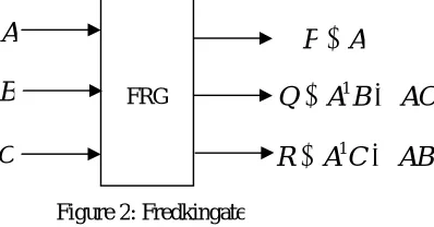
In figure 2, the block diagram of the three inputs (A, B, C) and three output (P, Q, R) Fredkin gate.
Figure 3 shows the Peres gate. A portion of the 4x4 doors are intended for executing some imperative combinational capacities notwithstanding the fundamental capacities. The vast majority of the aforementioned entryways can be utilized as a part of the outline of reversible adders.
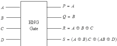
The HNG gate, presented in fig, produces the followinglogical output calculations:
A
P
(1)B
Q
(2)C
B
A
R
(3))
(
).
(
A
B
C
AB
D
S
(4)A
P
FGA
B
Q
A
B
AC
B
A
Q
1
C
B
A
AB
C
A
R
1
FRG
A
P
B
A
Q
C
B
A
C
B
A
R
.
Peres Gate
A
P
Figure 1: Feynman gateFigure 2: Fredkingate
The quantum cost and delay of the HNG is 6. At the point when D = 0, the consistent estimations created on the R and S yields are the required total and complete operations for a full snake. The quantum representation of the HNG is exhibited in Fig. 4.
A new programmable 4x4 reversible logic structure - Peres And-Or(PAOG) gate – is presented which produces outputs
A
P
(5)B
A
Q
(6)C
AB
R
(7))
)
((
).
(
AB
C
C
A
B
D
S
(8)Fig. 5 shows the block diagram of the PAOG gate. This gate is an extension of the Peres gate for ALU realization.
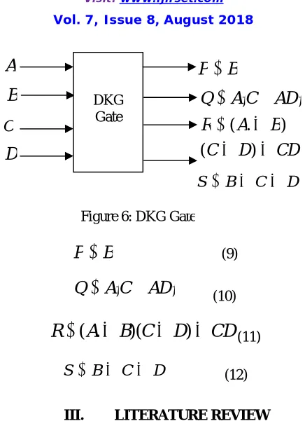
Several 4x4 gates have been described in the literature targeting low costand delay which may be implemented in a programmable manner to produce a high number of logical calculations. The DKG gate produces the followinglogical output calculations:
A
P
B
A
Q
C
AB
R
)
(
)
)
((
C
AB
D
B
A
S
A
B
C
D
PAOG
B
P
(9)D
A
C
A
Q
(10)
CD
D
C
B
A
R
(
.
)(
)
(11)D
C
B
S
(12)III. LITERATURE REVIEW
Gopi Chand Naguboina et al. (2017, [1]),reversible logic is the emerging field for research in present era. The aim of this paper is to realize different types of combinational circuits like full-adder, full-subtractor, multiplexer and comparator using reversible decoder circuit with minimum quantum cost. Reversible decoder is designed using Fredkin gates with minimum Quantum cost. There are many reversible logic gates like Fredkin Gate, Feynman Gate, Double Feynman Gate, Peres Gate, Seynman Gate and many more. Reversible logic is defined as the logic in which the number output lines are equal to the number of input lines i.e., the n-input and k-output Boolean function F(X1, X2, X3,…,Xn) (referred to as (n, k) function) is said to be reversible if and only if (i) n is equal to k and (ii) each input pattern is mapped uniquely to output pattern. The gate must run forward and backward that is the inputs can also be retrieved from outputs. When the device obeys these two conditions then the second law of thermo-dynamics guarantees that it dissipates no heat. Fan-out and Feed-back are not allowed in Logical Reversibility. Reversible Logic owns its applications in various fields which include Quantum Computing, Optical Computing, Nanotechnology, Computer Graphics, low power VLSI Etc., Reversible logic is gaining its own importance in recent years largely due to its property of low power consumption. The comparative study in terms of garbage outputs, Quantum Cost, numbers of gates are also presented. The Circuit has been implemented and simulated using Xilinx software.
Michael Nachigal et al. (2016, [2]), the design of encoder/decoder can be analyzed in terms of quantum cost, garbage outputs, constant inputs. Reversible computational work totally differs from traditional computation, as it preserves information while manipulating it. Various reversible combinational and sequential designs have been implemented based on reversibility nature of the circuit. Very little focus has been done on reversible encoder/decoder design. The author proposed a novel design, where 2:4 encoder and decoder are implemented by using Friedkin gates whose quantum cost associated is 5 instead of peres gate whose quantum cost is 4. This work also represents the improvement in garbage output that is added to a multiple output function to make it reversible. Implemented or proposed design for decoder/encoder improves over existing design in terms of performance metrics except for the delay.
Md. Shamsujjoha et al. (2015, [3]), by stating that a fault tolerance gate (F2G) itself work as 2 to 1 reversible decoder. A Figure 6: DKG Gate
C
B
A
D
B
P
DKG GateD
A
C
A
Q
CD
D
C
B
A
R
)
(
)
.
(
D
C
B
extended to 3 to 8 reversible decoder using FRG gates and Feynman double gate. Similarly a reversible 4 to 2 encoder design which behaves like a traditional encoder i.e., exactly one of its four inputs will have the value of logical 1 at any point. The design has zero constant inputs and two garbage outputs. Constructed circuits can detect any type of single bit error for stuck-at fault. This technique also minimizes the garbage outputs during the process of conversion to testable, but the design is not much optimized in terms of quantum gates, constant input, and delay.
Nusrat Jahan Lisa et al. (2014, [4]), designs a 2 to 4 decoder, which generates all four necessary AND functions using 1 Peres gate and 3 CNOT gate, therefore a total number of quantum gates are seven. The design can be extended to 3 to 8 decoder using 2 to 4 decoder circuit and four Fredkin gates and 4 to 16 decoder circuit using three 2 to 4 decoder and eight fredkin gates. Also, represent the properties of n to the 2n reversible decoder with a generalized algorithm. Design greatly improves over a conventional design of decoder can be constructed to improve the garbage output comes at the cost of a slightly higher quantum cost. Arvind Kumar et al. [9] concluded that the 2 to 4 decoder uses fredkin gates. Since all three fredkin gates are reversible in nature thus having less power dissipation. Design can be extended up to n to 2n decoder. A 4 to 16 decoder has been designed uses 15 constant inputs and 4 garbage outputs. This work is quite effective in terms of performance with three fredkingate; total delay will be more which in turn leads to more power dissipation claims that this design is not an effective approach.
IV. SIMULATION TOOL
Environment setup is the work environment or tools on which result analysis has been done for Xilinx 6.2i. Xilinx is the very strong software tool to analysis and simulate the complex circuits. There are so many versions for Xilinx software such as 6.1i, 9.1i, 10.2i, 13.1i and 14.2i. Generally two programming language are using VHDL and Verilog.
VHDL is an acronym for VHSIC hardware description language (VHSIC is an acronym for very high speed integrated circuits). It is a hardware description language that can be used to model a digital system at many levels of absorption ranging from the algorithm level to the gate level [14]. VHDL allows users or programmers to use certain blocks which comprise of certain set of sequential statements. One such block is called a process. The (<=) operator, it is called the assignment operator and is used only for assigning values to signals. For variables the operator used is (≔).
Some chief terms that are used at the basic level are: - Libraries, Data types, Signals, Variables, Entity, and Architecture. Other important terms for the VHDL program such as process, component, function, procedures and state diagrams are used in programming.
Reversible Gate Parameter:-
Gate Count (GC): The number of gates used to realize reversible circuit
Garbage Outputs (GO): The number of unused outputs in a reversible logic. The inputs regenerated at the outputs are not garbage outputs.
Ancilla Inputs (AI): The number of input kept constant at either 0 or 1.
Delay : It corresponds to number of primitive quantum gates in the critical path of the circuit.
Quantum Cost:- Quantum cost is defined, as the number of basic quantum gates like controlled-NOT, Controlled V+, Controlled V and NOT gate.
V. EXPECTED OUTCOMES
The resulting VHDL simulation models can then be used as building blocks in larger circuits (using schematics, block diagrams, or system-level VHDL descriptions) for the purpose of simulation.
1. Design 64-bit, 32-bit, 16-bit, 8-bit, 4-bit and 2-bit encoder and decoder using different types of reversible gate. 2. Design different types of programmable reversible gate and compared.
5. All the modules design to different device family i.e. Spartan-3, Virtex-4 and Virtex-7.
VI. CONCLUSION
This thesis mainly focuses on a novel design of reversible processor components. Internal architecture components I;e, ALU, CU, register files and PC having better performance with proposed circuitry as compared to previous counterparts. Also, registers and the memory for program and data fall into the category of improved performance with reduced delay. Memory access pattern, execution, and complexity of instruction are kept in mind improve the execution time by using Harvard architecture instead of von Neumann. Power dissipation is also less about negligible since an overall system is designed using reversible nature of logics. With all above demonstration, using proposed designs improve the performance of CPU and execution time will be faster.
REFERENCES
[1] Gopi Chand Naguboina and K. Anusudha, “Design and Synthesis of Combinational Circuits Using Reversible Decoder In Xilinx”, IEEE International Conference on Computer, Communication, and Signal Processing (ICCCSP-2017).
[2] Hatkar A. P., Hatkar A. A. and Narkhede N. P., “ASIC Design of Reversible Multiplier Circuit”, International Conference on Electronic Systems, Signal Processing and Computing Technologies, pp. 01-05, 2014 IEEE.
[3] Matthew Morrison and Nagarajan Ranganathan, “Design of a Reversible ALU based on Novel Programmable Reversible Logic Gate Structures”, IEEE Computer Society Annual Symposium on VLSI, pp. 01-06, 2013 IEEE.
[4] Mr. Abhishek Gupta, Mr. UtsavMalviya and Prof. Vinod Kapse, “Design of Speed, Energy and Power Efficient Reversible Logic Based Vedic ALU for Digital Processors”, IEEE Computer Society Annual Symposium on VLSI, vol. 12, Issue 05, pp. 3456-3463, 2012.
[5] H. Thapliyal and N. Ranganathan, "Design of Efficient Reversible Binary Subtractors Based oNew Reversible Gate," Processing of the Computer Society Annual Symposium on VLSI, pp. 01-06, 2009.
[6] Matthew Morrison and NagarajanRanganathan, “Design of a Reversible ALU based on Novel Programmable Reversible Logic Gate Structures”, 2013 IEEE Computer Society Annual Symposium on VLSI.
[7] LekshmiViswanath and Ponni. M, “Design and Analysis of 16 Bit Reversible ALU”, ISSN: 2278-0661 Volume 1, Issue 1 (May-June 2012), PP 46-53
[8] Akanksha Dixit and Vinod Kapse, “Arithmetic & Logic Unit (ALU) Design using Reversible Control Unit”, International Journal of Engineering and Innovative Technology (IJEIT) Volume 1, Issue 6, June 2012.
[9] Mr. Abhishek Gupta, Mr. UtsavMalviya and Prof. Vinod Kapse, “Design of Speed, Energy and Power Efficient Reversible Logic Based Vedic ALU for Digital Processors”, 2012 IEEE Computer Society Annual Symposium on VLSI.
[10]H. Thapliyal and N. Ranganathan, "A New Reversible Design of BCD Adder," To appear in Proc. Design Automation and Test in Europe (DATE), 2011.