Design of Power Efficient Memristor Based
SRAM Using MTCMOS Technique
Reena S. Wasankar, Ashish E. Bhande, Dr. U. A. Kshirsagar
M.E. Student, Dept. of Electronics & Telecommunication Engineering, HVPM COET, Amravati, Maharashtra, India
Asst. Professor, Dept. of Electronics & Telecommunication Engineering, HVPM COET, Amravati, Maharashtra, India
Professor & HoD, Dept. of Electronics & Telecommunication Engineering, HVPM COET, Amravati, Maharashtra,
India
ABSTRACT: In today’s world demand of low power devices is increasing and the reason behind this is scaling of CMOS technology. Due to the scaling, size of the chip decreases and number of transistor in system on chip (SOC) increases and this phenomenon also apply on memories that are used in SOC. Memories are the power hungry devices in any digital system but today no digital system can be completed without memories. However, the transistor miniaturization also introduces many new challenges in very large-scale integrated (VLSI) circuit design. So in future the need of low power memories is increasing and to design low power memories leakage power is attentive parameter to design low power devices because it plays a major role in increasing the total power consumption of the devices. In this project, MTCMOS (Multi Threshold CMOS) technique is used recently it is very famous in academia and industry. It is a power reducing technique that helps in reducing leakage power in the SRAM by turning of the inactive circuit domains. Designing and calculation of parameters of simple SRAM, Memristor based SRAM and MTCMOS based Memristor SRAM has been done with CMOS Design tool and that will do at 45 nm technology.
KEYWORDS: Low power, Speed, SRAM, Non Volitle Memory,CMOS, Memristor,MTCMOS.
I. INTRODUCTION
Since the invention of the first Integrated Circuit (IC), silicon technology scaling down continues to meet the increasing demands for higher functionality and better performance at a lower cost. The advances in VLSI integration technology have made it possible to put a complete System on a Chip (SoC) which facilitates the development of portable systems. The growing demand for VLSI circuits the leakage current on the oxide thickness is becoming a major challenge in deep-sub-micron CMOS technology. In deep submicron technologies, leakage power becomes a key for a low power design due to its ever increasing proportion in chip’s total power consumption.Motivated by emerging battery-operated application on one hand and shrinking technology of deep sub micron on the other hand, leakage power dissipation is playing a significant role in the total power dissipation as threshold voltage becomes low. Due to the trade-off between power, area and performance, various efforts have been done. So the low power devices are the first choice of VLSI designers and these low power devices fulfill the goal of the systems. The value of power that can be dissipated from the power supply mathematically is represented as-
(1)
Where is average power, T is time, I is current and V is voltage.In future demand of battery operated portable systems in electronic field increases such as mobile phones, laptops, notebook computers, Personal Digital Assistants (PDAs), military equipments and other handheld devices in electronic field Low power system and these systems to store their data use memories.
The capacitor can be either charged or discharged. These two states are 0 and 1. It stores each bit of data in a separate capacitor within IC. It has to be dynamically refreshed all of the time. In SRAM flip-flop holds each bit of memory. Flip-flop for a memory cell takes 4 or 6 transistors along with some wiring but never has to be refreshed. SRAM and DRAM holds data in different ways. SRAM can read and wright data faster than DRAM. SRAM consumes less power than DRAM. The main reason to use SRAM is its speed advantage over the main memory that uses DRAM. Now a day the aggressive scaling of the transistor size drastically affects SRAM devices, which are widely used in many digital chips such as cache and so on. In SRAM cell does not need refreshing technique and it is volatile in nature that means when power is plugged in, data is stored and as the power is plugged out data will get lost other qualities of SRAM is it use number of transistors to store a single bit in system on chip (SOC) and it reduces the delay between the processor and memories. These advantages of SRAM are used to design portable systems that is why low power SRAM is very demand full in handheld devices.
Memristor was invented by Leon O. Chua in 1971 and according to Chua Memristor is a fourth non-linear passive two terminal electrical component with variable resistance also called as memristance that give relation between flux
(Φm) and charge (q) in which the magnetic flux (Φm) between the terminals is a function of the amount of electric charge q that has passed through the device and it is denoted by M and its unit is Ω and mathematically represented as-
(2)
Where M is the Memristor, Φm is the magnetic flux and q is the charge. First Memristor was manufactured in HP labs
by the R. Stanley Williamsin 2008. Memristor is a new type of device that can be used to design memristive system, devices and memories. Resistance of memristor depends on the magnitude and polarity of the voltage applied to it. It has nonlinear relationship between voltages and current which is similar to memory devices. Using the Memristor technique in simple SRAM reduces the total powerand leakage power.
In this paper also apply MTCMOS technique on Memristor based SRAM it is a power switch and an effective circuit-level technique. It is a variation of CMOS chip technology which has transistors with multiple threshold voltages (Vth) in order to optimize delay or power. It uses sleep transistors which improves the speed of the devices and decrease the power remarkable. It is a power reducing technique that helps in reducing leakage power in the SRAM during standby mode and attains high speed in active mode. Therefore in this paper designed MTCMOS based Memristor SRAM. Memristor and MTCMOS have been used to designed low power SRAM.
II. LITERATURE REVIEW
Thangamani.V [2] presented by the approach to design memristor based nonvolatile 6-T static random access memory (SRAM) and analysis the circuit performance with conventional 6-T SRAM cell in order to prove the parameter optimizations. Then we address the memristor-based resistive random access memory (MRRAM) which is similar to that of static random access memory (SRAM) cell and we compare the nonvolatile characteristics of MRRAM with SRAM cell.
Uma Nirmal, Geetanjali Sharma, Yogesh Sharma [3] presented by the main objective is to provide new low power solution for Very Large Scale Integration (VLSI) designers. MTCMOS is an effective circuit-level technique that provides a high performance and low-power design by utilizing both low and high-threshold voltage transistors. MTCMOS technique has been proposed in this paper and the proposed technique has small power dissipation as compared to CMOS technique. Simulations based on BSIM 3V3 180nm CMOS technology. It shows 4 bit adders of the proposed technique have low power dissipation as compared CMOS technique.
Mika Kutila, Ari Paasio and Teijo Lehtonen [6] presented by the 8T SRAM and 6T SRAMmemory cells are compared in order to establish guidelines for choosing SRAM cell constructions for NTC systems. 8T SRAM is traditionally concerned as a more reliable memory cell, but we have managed to design 6T SRAM which executes read operation with an acceptaple reliability; read being the most vulnerable operation of conventional 6T SRAM cell. Also, our 6T SRAM cell has 31% smaller area and smaller power consumption.
III.IMPLEMENTATION 6T SRAM
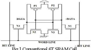
The static RAM is a very important class of memory. It consists of two cross-coupled inverters, which form a positive feedback with two possible states. Fig.1. shows the conventional SRAM cell. Word line is used for enabling the access transistors N1 and N4 for write operation. BL and ~BL lines are used to store the data and its compliment. Both the bit lines (BL and ~BL) are used to transfer the data during the read and write operations in a differential manner. To have better noise margin, the data signal and its inverse is provided to BL and ~BL respectively. For write operation one BL is High and the other bit line remain in low condition. It uses six transistors in Fig 1. to store and access one bit. The four transistors in the centre form two cross-coupled inverters. It has 2 pull up PMOS and 2 NMOS pull down transistors as two cross coupled inverters and two 2 NMOS access transistors to access the SRAM cell during Read and Write operations.
Fig.1 Conventional 6T SRAM Cell
Layout Design of 6-Transistor SRAM cell
Fig 2. layout design of 6T SRAM cell
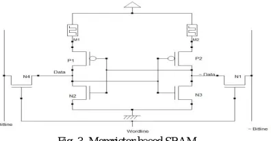
Memristor based SRAM
Fig. 3 Memristor based SRAM
Memristor works as a switch like transistor except that Memristor is a two terminal device while transistor is a three terminal device. Memristor is manufactured by two thin layers and these layers are sandwiched between platinum nano-wires and layers are also in nanometer size. These layers are of doped TiO2-x and another is undoped TiO2. Change in resistance occurs in these layer because one TiO2 layers receivesoxygen ions and other TiO2 layer losses the oxygen ions i.e. movement of mobile ionic charge inside the TiO2 layer result in change in Memristor resistance. That is why it is called variable resistance and it is used in designing of memories. This is the reason that Memristor can help in reducing total power in the Memristor based SRAM. In this paper, Memristor based 6T SRAM has been designed. Fig3. shows the Memristor based 6T SRAM cell. Memristor M1 is connected between Vdd supply and at centre point of 2 PMOS transistor. Using the Memristor technique in simple SRAM reduces the total power and leakage power.
Layout Design of Memristor based SRAM
Fig 4. shows the layout of Memristor based SRAM. The supply used Vdd is a DC supply of 0.4V.
Fig 4. Layout of Memristor based SRAM
MTCMOS
Fig 5.Memristor based SRAM using MTCMOS
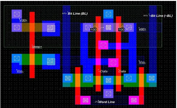
Layout Design of Memristor based SRAM using MTCMOS technique
Fig 6 shows the layout of Memristor based SRAM using MTCMOS technique. The supply used Vdd is a DC supply of 0.4V. The technology used is 45 nm technology.
Fig 6. Layout Memristor based SRAM using MTCMOS technique
In fig 2, fig 4 and fig 6 uses, Bit line is a clock of 0.40 V as a level 1 and 0.0 V as level 0 with time low(tl) = 0.045ns ns, Rise time (tr)=0.005 ns, high time (th) = 0.045 ns and fall time (tf)=0.005. Bit line bar is a clock of 0.40 V as a level 1 and 0.0 V as level 0 with time low(tl) = 0.450 ns, Rise time (tr)=0.005 ns, high time (th) = 0.450 ns and fall time (tf)=0.005 ns. Data line is a clock of 0.40 V as a level 1 and 0.0 V as level 0 with time low(tl) = 0.045 ns, Rise time (tr)=0.005 ns, high time (th) = 0.045 ns and fall time (tf)=0.005. Data bar line is a clock of 0.40 V as a level 1 and 0.0 V as level 0 with time low(tl) = 0.450 ns, Rise time (tr)=0.005 ns, high time (th) = 0.450 ns and fall time (tf)=0.005ns. Word line is a clock of 0.40 V as a level 1 and 0.0 V as level 0 with time low(tl) = 0.450 ns, Rise time (tr)=0.005 ns, high time (th) = 0.450 ns and fall time (tf)=0.005ns.
IV.SIMULATION RESULTS
Simulation result
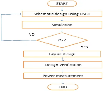
Every step of design follows the design flow of Microwind 3.1 software. The design methodology will be according to VLSI backend design flow. The main target is to design and analyze and verify operation of memory resistor. We simulate the proposed layout using the following design steps shown in the flow chart and obtained the simulation results. Following are the 4 steps.
3. CMOS layout for the proposed SRAM using VLSI backend. 4. Verification of CMOS layout and parameter testing
.
If the goal is achieved for all proposed parameter including detail verification, sing off for the design analysis and design will be ready for IC making. If detail verification of parameters would not complete then again follow the first step with different methodology. The operational voltage is usually from 0.2 V to 1.8 V, depending on the technology variant. In Microwind, it decided to fix VDD at 0.4 V in the cmos45nm. RUL rule file, which represents a compromise between all possible technology variations available for this 45-nm node. Effort has been taken to design Low Power, High performance memristor based SRAM cell using MTCMOS technology.
Fig7. Design Flow Chart
6T SRAM CELL
The simulation of the 6T SRAM cell on 45nmVLSI technology and obtained the corresponding results as shown in fig 8. To access a particular memory cell, the corresponding bit line and the corresponding word line must be activated (selected). Only one word line is activated (selected) at a time by raising its voltage to VDD. When applied logic 1 to word line, the data of the bit line get sampled means whatever the data bit line has get copied into data line. When applied logic 0 to word line, the data which previously get write on to the data line will now get read on data line and thus read-write cycle continues. The total power consumed by chip is 0.045μm.
Fig 8 Simulation for the 6T SRAM cell
Memristor based SRAM
to be stored either ‘0’ or ‘1’ is latched in. Also through appropriate cell or cells data is then read. Also the corresponding data and inverted data lines are shown in the following figure. The data line is at logic 0 and corresponding inverted data line is at logic 1.
Fig 9. Simulation for the Memristor based SRAM
3
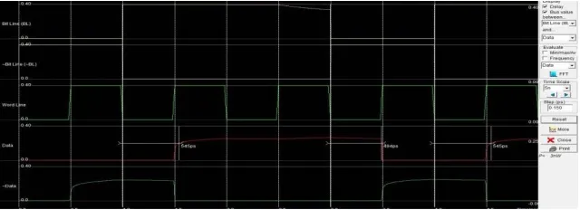
Memristor based SRAM using MTCMOS techniqueThe simulation of the Memristor based SRAM using MTCMOS technique cell is proposed in fig 10. To access a particular memory cell, the corresponding bit line and the corresponding word line must be activated (selected). Only one word line is activated (selected) at a time by raising its voltage to VDD. When applied logic 1 to word line, the data of the bit line get sampled means whatever the data bit line has get copied into data line. When applied logic 0 to word line, the data which previously get write on to the data line will now get read on data line and thus read-write cycle
continues. The total power consumed by chip is 0.003μm.
Fig 10 Simulation for Memristor based SRAM using MTCMOS technique
Table 1 Parameters of Memory Cell Using 45 nm CMOS Technology Memory Cell
Area (μm2 )
Delay Time
6T SRAM cell (power) Write time
(rise time) ps
Read time (fall time)
ps
Simple SRAM 1.153125 512 499 0.045 uW Memristor based
SRAM
1.153125 545 494 0.010 uW
MTCMOS based Memristor
SRAM
Above Table representing area, dalay time and power of Simple SRAM, Memristor based SRAM and MTCMOS based Memristor
V. CONCLUSION AND FUTURE WORK
The proposed Memory is designed using 45 nm CMOS/VLSI technology with Microwind 3.1. The Software used in program allows us to design and simulate an integrated circuit at physical description level. The proposed designed Memristor based 6T SRAM cell with the help of MTCMOS techniques. It is non-volatile in nature because of Memristor. it increases the packing density and reduces the power in system on chip (SOC) these techniques helps in reducing the leakage power in the device without loss of stored data. SRAM takes large part of power & area, therefore to improve power & speed here we are designing Memristor based SRAM. MTCMOS is a power reducing technique that helps in reducing leakage power in the SRAM by turning of the inactive circuit domains.
Memristor based 6T SRAM and MTCMOS based 6T Memristor SRAM at 45 nm technology was designed and was determined which SRAM is better based on total power . According to result analysis and graphs it is concluded that MTCMOS based 6T Memristor SRAM is better than the simple 6T SRAM and Memristor based 6T SRAM. MTCMOS based 6T Memristor consume less power uses only 0.003 uW .
REFERENCES
1. Vijay Singh Baghel and Shyam Akashe, “Low power Memristor Based 7T SRAM Using MTCMOS Technique,” IEEE , Fifth International Conference on Advanced Computing & Communication Technologies in MP,India, 2015.
2. Thangamani.V, “Memristor-Based Resistive Random Access Memory: Hybrid Architecture for Low Power Compact Memory Design,”IISTE, Control Theory and Informatics ISSN 2224-5774 (Paper) ISSN 2225-0492 (Online) Vol.4, No.7, 2014.
3. Uma Nirmal, Geetanjali Sharma, Yogesh Sharma, “A Low Power High Speed Adders using MTCMOS Technique,” IJCEM International Journal of Computational Engineering & Management, Vol. 13, July 2011.
4. Nobuaki Kobayashi, Ryusuke Ito and Tadayoshi Enomoto, “A High Stability, Low Supply Voltage and Low Standby Power Six-Transistor CMOS SRAM,” IEEE 978-1-4799-7792-5/15/$31.00 ©2015
5. Farshad Moradi and Jens K. Madsen, “Robust Subthreshold 7T-SRAM Cell for Low-Power Applications,” IEEE,2014.
6. Mika Kutila, Ari Paasio and Teijo Lehtonen, “Comparison of 130 nm Technology 6T and 8T SRAM Cell Designs for Near-Threshold Operation,” IEEE ,978-1-4799-4132-2/14/$31.00 ©2014
7. G.-F. Wang, W. Kang, Y.-Q. Cheng, J. Nan, J.-O. Klein, Y.-G. Zhang, and W.-S. Zhao, “Low Power Computing Paradigms Based on Emerging Non-Volatile Nanodevices,” JOURNAL OF ELECTRONIC SCIENCE AND TECHNOLOGY, VOL. 12, NO. 2, JUNE 2014. 8. Amit Grover, “Low Power 7-T SRAM using 90 NM Technology with Tanner Tool,” IEEE, FirstInternational Conference on Artificial
Intelligence, Modelling & Simulation, 2013.
9. U. Supriy, K. Ramana Rao, “Design of Low Power CMOS Circuits using Leakage Control Transistor and Multi-Threshold CMOS Techniques,” IJCTA ,July-August,Vol 3 (4), 2012.
10. Bastien Giraud and Amara Amara, Andrei Vladimirescu, “A Comparative Study of 6T and 4T SRAM Cells in Double-Gate CMOS with Statistical Variation,” IEEE ,1-4244-0921-7/07 $25.00 © 2007.
11. Nikhil Raj, Rohit Lorenzo “An effective design technique to reduce leakage power” IEEE Students,” Conference on Electrical, Electronics and Computer Science, pp 1-4, March 2012 in Bhopal.