Area Decreased With Compact Size Multiplier
by Using Common Boolean Logic with Low
Power Dissipation
S.Sangeetha Priya, .N.Rajkumar
Assistant Professor, Dept. of Electronics and Communication, V.R.S College of Engineering and Technology,
Tamilnadu, India
Assistant Professor, Dept. of Information Technology, V.R.S College of Engineering and Technology,
Tamilnadu, India
ABSTRACT: Nowadays multiplier plays an vital role in today’s digital signal processing and other high performance system. With the help of multiplier nowadays various high speed, low power and compact system of VLSI implementation can be made. The conventional multiplier there is the reduction of delay, but the proposed multiplier will reduce the delay in each and every gate. By using the common Boolean logic, we can reduce the area,delay,power of the multiplier. And hence we can reduce the delay,area,power of each and every gates.
KEYWORDS: Digital signal processing, common Boolean Logic, conventional multiplier.
I.INTRODUCTION
The process of creating integrated circuits is by combining thousands of transistors into a single chip in the VLSI .there are many challenges in VLSI circuit which must be developed to make the VLSI in efficient manner. With the advances in the technology and also in the electronics, many researchers have tried and are trying for the various designs of multipliers which will offer for various targets such as high speed, low power consumption, regularity of layout, less area. The multiplication method is mainly based on Add and Shift algorithm. The performance of the multiplier which determines the main parameter is that adding the number of partial products in the parallel multiplier. To reduce the partial products the modified booth algorithm is one of the most popular algorithms. Then Wallace tree multiplier reduces the sequential adding stages. However the no of shifts between the partial products and the intermediate sums to be added will increase which may result in reduced speed by increasing the parallelism in multiplier.
II.EXISTING SYSTEM
The CSLA partitions the adder into several groups, each of which performs two addition operations parallel. So two copies of ripple carry adder act as carry evaluation per block to select stage. One copy evaluates the carry chain assuming the block carry is zero, While another to be one. Once the carry signals are finally computed the desired sum and the carry will be simply select from the multiplexer.
ISSN(Online): 2320-9801
ISSN (Print) : 2320-9798
I
nternational
J
ournal of
I
nnovative
R
esearch in
C
omputer
and
C
ommunication
E
ngineering
(An ISO 3297: 2007 Certified Organization)
Vol. 4, Issue 4, April 2016
The carry generation of ripple carry generation is done in four stages
1. Half sum generation (HSG)
2. Half carry generation(HCG)
3. Full sum generation(FSG)
4. Full carry generation(FCG)
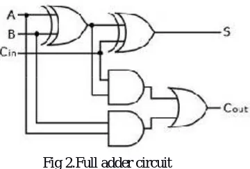
Fig 2.Full adder circuit
the circuit evaluation is done by total no of gates in the circuit and hence the circuit of multiplexer is given by,
Fig 3.Circuit diagram of 2:1 multiplexer
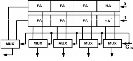
The conventional multiplier does the operation of multiplication. The conventional system circuit consists of 8 full adder and 4 half adder.CSLA is not efficient because of using the multiple pairs of ripple carry adders. To generate the partial sum and carry by considering the carry inputs cin=0 and cin=1,then the final sum and the carry is selected by the multiplexer.
Fig 4. Conventional adder structure
Here the inputs are given as A0,A1,A2,A3,B0,B1,B2,B3.The desired partial products are mentioned as S0,S1,S2,S3,S4,S5,S6,S7.FA is the full adders in the circuit .HA is the half adder in the circuit. We are going to replace the full adders by using the common Boolean logic.
III.PROPOSED SYSTEM
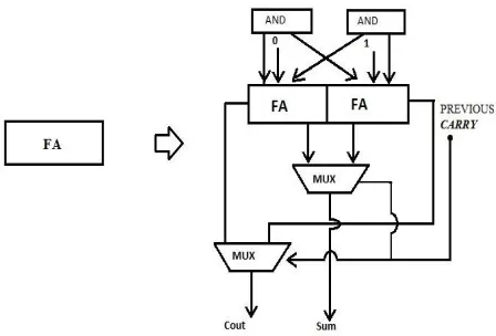
The delay of the circuit is reduced initially by replacing the full adders in the conventional CSLA and hence
the process is more efficient by the replacement. To overcome this problem we introduce CBL in proposed methodology;
ISSN(Online): 2320-9801
ISSN (Print) : 2320-9798
I
nternational
J
ournal of
I
nnovative
R
esearch in
C
omputer
and
C
ommunication
E
ngineering
(An ISO 3297: 2007 Certified Organization)
Vol. 4, Issue 4, April 2016
Fig 6. Replacement of conventional full adder with proposed full adder
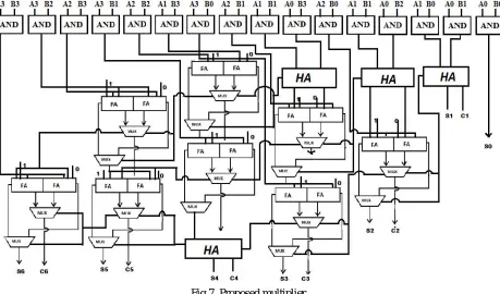
By analysing the truth table of a single bit full adder the output of summation signal as carry –in signal is logic ¨0¨is the inverse of itself as carry-in signal is logic¨1¨.to share the common Boolean logic term it only needs to implement one OR gate with one INVERTER gate to generate the carry signal and summation signal pair. The truth table and the circuit of proposed system is given below
Fig 7. Proposed multiplier
IV. SIMULATION AND RESULTS
ISSN(Online): 2320-9801
ISSN (Print) : 2320-9798
I
nternational
J
ournal of
I
nnovative
R
esearch in
C
omputer
and
C
ommunication
E
ngineering
(An ISO 3297: 2007 Certified Organization)
Vol. 4, Issue 4, April 2016
Output by using microwind to find the power dissipation of the circuit is shown below .The following diagram represents the four bit conventional multiplier and the proposed system by using common Boolean logic by using the microwind.
4 BIT MULTIPLIER OUTPUT
OUTPUT COMPARISON BETWEEN MULTIPLIERS
FACTORS 4 BIT MULTIPLIER 4 BIT CONVENTIONAL MULTIPLIER 4 BIT PROPOSED MULTIPLIER AND GATE NOT GATE XOR GATE OR GATE HALF ADDER FULL ADDER MULTIPLEXER 16 00 00 00 04 08 00 16 00 00 00 04 16 16 24 08 08 08 04 00 16
NO. OF GATES
ISSN(Online): 2320-9801
ISSN (Print) : 2320-9798
I
nternational
J
ournal of
I
nnovative
R
esearch in
C
omputer
and
C
ommunication
E
ngineering
(An ISO 3297: 2007 Certified Organization)
Vol. 4, Issue 4, April 2016
V.CONCLUSION
A new multiplier is designed by using CBL logic it achieved area and speed higher than that of the existing multiplier, with an area requirement comprisable with the CSLA demonstrated .These multiplier could propagate a carry signal and sum signal with low power dissipation and propagation delay. In addition because of adopted basic logic and layout strategy number of clock cycle required for completing the elaboration was limited and hence it reduce the power dissipation. The area and the propagation delay should be reduced by using CBL logic. Finally the multiplier has been designed efficiently in terms of low area, less propagation delay and low power dissipation.
REFERENCES
[1] Shin-Kai Chen, Chih-Wei Liu, Member, IEEE, Tsung-Yi Wu, and An-Chi Tsai,” Design and Implementation of High-Speed and Energy-Efficient Variable-Latency Speculating Booth Multiplier (VLSBM)”, IEEE transactions on circuits and systems regular papers, vol. 60, no. 10, october 2013
[2] B.Ramkumar, . and Harish M Kittur, (2012) 'Low Power and Area Efficient Carry Select Adder', IEEE Transactions on Vel), Large Scale
Integration (VLSI) Systems, pp.I-S.
[3] I- Chyn Wey, Cheng-Chen Ho, Yi-Sheng Lin, and ChienChang Peng 'An Area-Efficient Can), Select Adder Design by Sharing the Common Boolean Logic Term' Proceeding on the international Multiconference of eng. and computer scientist 2012 , IMECS 2012.
[4] G.Shyam Kishore, “A Novel Full Adder with High Speed Low Area”, 2nd National Conference on Information and Communication Technology (NCICT) 2011,Proceedings published in International Journal of Computer Applications® (IJCA).
[5] Deepa Sinha, Tripti Sharma, k.G.Sharma, Prof.B.P.Singh, “Design and Analysis of low Power 1-bit Full Adder Cell”,IEEE, 2011.
[6] Ning Zhu, Wang Ling Goh, Weija Zhang, Kiat Seng Yeo, and Zhi Hui Kong, “Design of Low-PowerHigh-Speed Truncation-Error-Tolerant Adder and Its Application in Digital Signal Processing”, IEEE Transactions on Very Large Scale Integration (VLSI) Systems, Vol.
18, No. 8, August 2010.
[7] Padma Devi, Ashima Girdher and Balwinder Singh, “Improved Carry Select Adder with Reduced Area and Low Power Consumption”,
International Journal of Computer Application,Vol 3.No.4, June 2010
[8] Y. He, C. H. Chang, and 1. Gu, "An area efficient 64-bit square root can),-select adder for low power applications," in Proc. IEEE Int.
Symp. Circuits Syst., 2005, vol. 4, pp. 4082-4085.
[9] O. T. Chen, S. Wang, and Y.-W. Wu, “Minimization of switching activities of partial products for designing low-power multipliers,”
IEEE Trans. Very Large Scale Integr. (VLSI) Syst., vol. 11, no. 3, pp. 418–433, Jun. 2003.
[10] K. Rawat, T. Darwish, and M. Bayoumi, "A low power and reduced area carry select adder", The 45th Midwest Symposium on Circuits
and Systems., vol. 1, pp.467-470, 2002.