ISSN(Online): 2320-9801
ISSN (Print): 2320-9798
I
nternational
J
ournal of
I
nnovative
R
esearch in
C
omputer
and
C
ommunication
E
ngineering
(An ISO 3297: 2007 Certified Organization)
Vol. 3, Issue 7, July 2015
An Efficient Low Power Multiplier Based on
Shift-and-Add Architecture
Mahesh Gajula, N. Rushi Shrunga
M.Tech (VLSI), Dept of ECE, Avanthi Scientific Technology& Research Academy, Hyderabad, India
Associate Professor, Dept of ECE, Avanthi Scientific Technology & Research Academy, Hyderabad, India
ABSTRACT: In this paper, an efficient low-power structure called bypass zero, feeding directly to An Efficient Low Power Multiplier based on shift-and-add multipliers is proposed. This architecture derives for lowers the switching activity of conventional multipliers. The modifications made to the multiplier which multiplies by include the removal of the shifting of the register and direct feeding to the adder, It bypasses the adder whenever possible, by using The ring counter instead of a binary counter and removal of the partial product shift. In this architecture we make use of a low-power ring counter proposed. The Simulation results for 32-bit radix-2 multipliers show that the Very an Efficient Low architecture and lowers the total switching activity up to 76% and power consumption up to 30% than to the conventional architecture. The proposed Architecture of multiplier can be used for low-power applications and where the speed is not a primary design parameter
KEYWORDS: Hot-block ring counter, low-power multiplier, low-power ring counter, shift-and-add multiplier, switching activity reduction.
I. INTRODUCTION
MULTIPLIERS are among the fundamental components of many digital systems and, hence, their power dissipation and speed are of prime concern. For portable applications where the power consumption is the most important parameter, one should reduce the power dissipation as much as possible. One of the best ways to reduce the dynamic power dissipation, henceforth referred to as power dissipation in this paper, is to minimize the total switching activity, i.e., the total number of signal transitions of the system.Many research efforts have been devoted to reducing the power dissipation of different multipliers. The largest contribution to the total power consumption in a multiplier is due to generation of partial product. Among multipliers, tree multipliers are used in high speed applications such as filters, but these require large area. The carry-select-adder (CSA) based radix multipliers, which have lower area overhead, employ a greater number of active transistors for the multiplication operation and hence consume more power. Among other multipliers, shift-and-add multipliers have been used in many other applications for their simplicity and relatively small area requirement. Higher-radix multipliers are faster but consume more power since they employ wider registers, and require more silicon area due to their more complex logic.
ISSN(Online): 2320-9801
ISSN (Print): 2320-9798
I
nternational
J
ournal of
I
nnovative
R
esearch in
C
omputer
and
C
ommunication
E
ngineering
(An ISO 3297: 2007 Certified Organization)
Vol. 3, Issue 7, July 2015
In this work, we propose modifications to the conventional architecture of the shift-and-add radix-2 multipliers to considerably reduce its energy consumption. This paper is organized as follows: toward a low power shift-and-add multiplier hot block ring counter results.
II. TOWARD A LOW POWER SHIFT-AND-ADD MULTIPLIER
A. Main Sources of Switching Activity
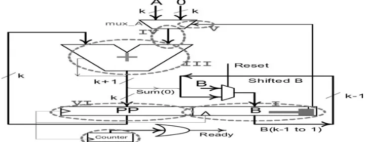
The architecture of a conventional shift-and-add multiplier, which multiplies by is shown in Fig. 1 [4]. There are six major sources of switching activity in the multiplier. These sources, which are marked with dashed ovals in the figure, are: (a) shifts of the B register (b) activity in the counter; (c) activity in the adder; (d) switching between “0” and A in
the multiplexer; (e) activity in the mux select controlled by B(0); and (f) shifts of the partial product (PP) register. Note
that the activity of the adder consists of required transitions (when is nonzero) and unnecessary transitions (when is zero).
By removing or minimizing any of these switching activity sources, one can lower the power consumption. Since some of the nodes have higher capacitance, reducing their switching will lead to more power reduction. As an example, is the selector line of the multiplexer which is connected to gates for a -bit multiplier. If we somehow eliminate this node, a noticeable power saving can be achieved.
Next, we describe how we minimize or possibly eliminate these sources of switching activity B. Proposed An Efficient
Low Power Multiplier:
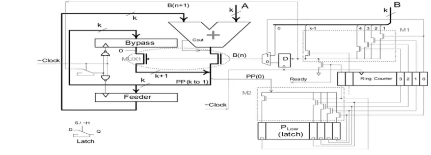
To derive a low-power architecture, we concentrate our effort on eliminating or reducing the sources of the switching activity discussed in the previous section. The proposed architecture which is shown in Fig. 2.
.
Fig. 2. Proposed An Efficient low power Multiplier architecture.
1) Shift of the B Register: In the traditional architecture (see Fig. 1),to generate the partial product, is used to decide
between and 0. If the bit is “1”, should be added to the previous partial product, whereas if it is “0”, no addition
ISSN(Online): 2320-9801
ISSN (Print): 2320-9798
I
nternational
J
ournal of
I
nnovative
R
esearch in
C
omputer
and
C
ommunication
E
ngineering
(An ISO 3297: 2007 Certified Organization)
Vol. 3, Issue 7, July 2015
current partial product is added to (when is one) or to 0 (when is zero). This leads to unnecessary transitions in the adder when is zero. In these cases, the adder can be bypassed and the partial product should be shifted to the right by one bit. This is what is performed in the proposed architecture which eliminates unnecessary switching activities in the
adder. As shown in Fig. 2, the Feeder and Bypass registers are used to bypass the adder in the cycles where is zero. In
each cycle, the hot bit of the next cycle is checked. If it is 0, i.e., the adder is not needed in the next cycle, the Bypass
register is clocked to store the current partial product. If is 1, i.e., the adder is really needed in the next cycle, the Feeder register is clocked to store the current partial product which must be fed to the adder in the next cycle. Note that to
select between the Feeder and Bypass registers we have used NAND and NOR gates which are inverting logic,
therefore, the inverted clock is fed to them. Finally, in each cycle. Determines if the partial product should come from the Bypass register or from the Adder output.
In each cycle, when the hot bit is zero, there is no transition in the adder since its inputs do not change. The reason is
that in the previous cycle, the partial product has been stored in the Bypass register and the value of the Feeder register,
which is the input of the adder, remains unchanged. The other input of the adder is , which is constant during the multiplication. This enables us to remove the multiplexer and feed input directly to the adder, resulting in a noticeable power saving. Finally, note that the BZ-FAD architecture does not put any constraint on the adder type. In this work, we have used the ripple carry adder which has the least average transition per addition among the look ahead, carry skip, carry-select, and conditional sum adders.
3) Shift of the PP Register: In the conventional architecture, thepartial product is shifted in each cycle giving rise to transitions. Inspecting the multiplication algorithm reveals that the multiplication may be completed by processing the most significant bits of the partial product, and hence, it is not necessary for the least significant bits of the partial product to be shifted. We take advantage of this observation in the BZ-FAD architecture. The lower half of the partial product, we use latches (for a -bit multiplier). These latches are indicated by the dotted rectangle in Fig. 2. In the first
cycle, the least significant bit PP(0) of the product becomes finalized and is stored in the right-most latch of . The ring
counter output is used to open (unlatch) the proper latch. This is achieved by connecting the line of the latch to the bit of the ring counter which is “1” in the cycle. In this way, the latch samples the value of the bit of the final product. In the subsequent cycles, the next least significant bits are finalized and stored in the proper latches. When the last bit is stored in the left-most latch, the higher and lower halves of the partial product form the final product result.
In brief, from the six sources of activity in the multiplier, we have eliminated the shift of the B register, reduced the activities of the right input of the adder, and lowered the activities on the multiplexer select line. In addition, we have minimized the activities in the adder, the activities in the counter, and the shifts in the PP (partial product) register. The proposed architecture, however, introduces new sources of activities. These include the activities of a new multiplexer which has the same size as that of the multiplexer of the conventional architecture. Note that the higher part of the partial product in both architectures has the same activity. Adder which has the least average transition per addition among the look ahead, carry skip, carry-select, and conditional sum adder.
II. HOT BLOCK RING COUNTER
In the proposed multiplier, we make use of a ring counter the architecture of which is described in this section. In a ring counter always a single “1” is moving from the right to the left. Therefore in each cycle only two flip-flops should be clocked. To reduce the switching activity of the counter, we propose to partition the counter into blocks which are clock-gated with a special multiple-bit clock gating structure shown in Fig. 4, whose power and area overheads are
independent of the block size. In the proposed counter, called HotBlock ring counter fewer superfluous switching
ISSN(Online): 2320-9801
ISSN (Print): 2320-9798
I
nternational
J
ournal of
I
nnovative
R
esearch in
C
omputer
and
C
ommunication
E
ngineering
(An ISO 3297: 2007 Certified Organization)
Vol. 3, Issue 7, July 2015
Fig. 3. Hot Block architecture for a 16-bit ring counter. The ring counter is partitioned into blocks of size only two clock gators are shown.
We have utilized the property that in each cycle, the outputs of all flip-flops, except for one, are “0”. Thus in the partitioned ring counter of Fig. 3, there is exactly one block that should be clocked we call this block the Hot Block. Therefore, for each block, the clock gating structure (CG) should only know whether the “1” has entered the block and has not yet left it. The CG starts passing the clock pulses to the block once the “1” appears at the input of the first flip-flop of the block. It shuts off the clock pulses after the “1” leaves the left-most flip-flip-flop of the block.
Fig. 4. Cock gating structure used in the proposed architecture.
The clock gating structure (CG) proposed for the Hot Block ring counter is shown in Fig. 4. It is composed of a multiplexer , a NAND gate, and a resettable latch. In this work, the multiplexers are implemented with transmission
gates. In addition to the Reset and 0 signals, there are two other signals called Entrance and Exit, coming from the
neighboring left and right blocks. These are usedto determine whether the “1” is present in the block to which the
output of the CG goes. When the active high Reset signal is “1”, the latch is reset which causes the value of the
Entrance signal to be placed on the line of the latch through multiplexer M1.
ISSN(Online): 2320-9801
ISSN (Print): 2320-9798
I
nternational
J
ournal of
I
nnovative
R
esearch in
C
omputer
and
C
ommunication
E
ngineering
(An ISO 3297: 2007 Certified Organization)
Vol. 3, Issue 7, July 2015
This in turn causes the latch to read the Entrance signal, which was previously reset to “0”, since the whole ring
counter is reset and all the bits except the first are reset to “0”. After a sufficiently long interval, Reset goes to “0” and
since Entrance has a value of “0”, the latch keeps holding “0” on its output, forcing Clock-OUT to “1” after the CG is
reset. This condition should persist until the “1” is about to enter to the block.
Multiplexer plays the watchdog role. After the CG is reset, the selector line of multiplexer, has the value of “0” which
causes the Entrance signal to be selected (watch dogged) by this multiplexer. Theoutput of the latch is also connected
to the NAND gate which causes the input clock signal to be shut off (gated), after the CG is reset. The Entrance and
Exit signals have special meanings as follows. When “1”, Entrance means that the “1” is about to enter the block in the
nextcycle. This line is connected to the block input, namely, the input of the right-most flip-flop in the block, as shown
in Fig. 3. The Exit signal on the other hand indicates the “1” has left the block and hence it should no longer be clocked.
Notice that the Exit signal is connected to the output of the right-most flip-flop of the left hand block.
Once the Entrance signal becomes “1”, the sample and data-in lines of the latch are set to “1”.This causes multiplexer
to select (watch dog) the Exit signal which is “0”, since all cells of the ring counter except one, have the value of “0” in
them. Through multiplexer , the value of the Exit signal (“0”) goes to the line of the latch, which in turn causes the
latch to hold “1” (the value of the Entrance signal) on its output. From this moment on, the Exit signal is watch dogged
by multiplexer; in addition, clock pulses are no longer gated by the NAND gate. To reduce the layout area, we have used a NAND gate instead of an AND gate, and thus, the input clock signal to the clock gator should be the inverted
clock ( 0 in Fig. 4). In the cycles when the Entrance signal becomes “1”, no positive clock edges should appear at the
output of the clock gator; instead it should only prepare to pass clock pulses during the next clock cycles.
This is achieved by using the inverted clock signal; the flip-flops are positive-edge triggered, and hence, when the
Entrance signal, which is the output of some flip-flop, becomes “1” at a positive clock edge, the “0” (negative edge), meaning that no extra positive edge is produced at the clock gator output.
The clock pulses come to the clock gating structure, propagate through the NAND gate, and go to the block cells via
Clock-OUT, until the Exit signal becomes “1”. Then the line of the latch becomes “1” through multiplexer causing the
latch to read its input (the Entrance signal), which is ’0’ at this time. The “0” prop-agates through the latch and reaches
the selector line of multiplexer giving rise to the Entrance signal to be watch dogged again. The output of the latch,
which is “0” in this state, also forces the NAND gate to shut off the input clock pulses. Note that regardless of the block size, the proposed CG has a total of four inputs.
IV SIMULATION RESULTS
In this section, we present experimental results for the proposed ring counter and multiplier. We used Xilinxs for the synthesis. Since we have used a standard cell library for this technology, all pass-transistors have been replaced with buffers during the synthesis of the implementations.
A. Ring Counter
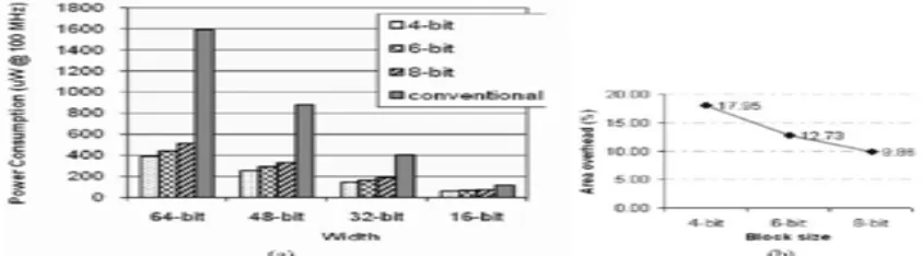
In Fig. 5(a), you can see the power consumption of the conventional and Hot Block (see Fig. 3) ring counters of 16-, 32-, 48-, and 64- bits. As seen in this diagram, the efficiency of the Hot Block architecture is more pronounced as the width of the ring counter increases; e.g., with the width of 64 bits, the conventional and Hot-Block consume 1591 and 389 W, respectively. The maximum power reduction is achieved for a 64-bit ring counter with blocks of 4 flip-flops, where a power reduction of 75% is achieved.
Now, we estimate the area overhead of the proposed ring counter. Note that the hot block clock gating structure (see Fig. 4) can be implemented using 18 transistors, which include 10 for the resettable latch, 4 for the multiplexer, and 4 for the NAND gate. As mentioned earlier, the multiplexers were implemented with transmission gates.
ISSN(Online): 2320-9801
ISSN (Print): 2320-9798
I
nternational
J
ournal of
I
nnovative
R
esearch in
C
omputer
and
C
ommunication
E
ngineering
(An ISO 3297: 2007 Certified Organization)
Vol. 3, Issue 7, July 2015
HDL Synthesis Report:
Macro Statistics
# Adders/Subtractors :1
17-bit adder :1 Counters :1
32-bit up counter : 1
# Registers : 18
1-bit register : 16
17-bit register : 1
32-bit register : 1 : 1
# Comparators : 2
33-bit comparator greater : 1
33-bit comparator lessequal : 1 # Multiplexers : 1
1-bit 16-to-1 multiplexer : 1
====================================
B. Multiplier
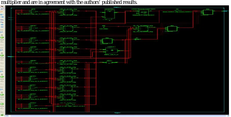
To evaluate the efficiency of the proposed architecture, we implemented three different Radix-2 16-bit multipliers corresponding to the conventional, and SPST architectures. The spurious power suppression technique (SPST) architecture is a very low-power tree-based. In general, array multipliers offer high speed and low power consumption. However they occupy a lot of silicon area. The SPST results presented in this paper are based on our implementation of this multiplier and are in agreement with the authors’ published results.
Fig. 6 A Schematic of 32-bit Multiplier Diagram.
ISSN(Online): 2320-9801
ISSN (Print): 2320-9798
I
nternational
J
ournal of
I
nnovative
R
esearch in
C
omputer
and
C
ommunication
E
ngineering
(An ISO 3297: 2007 Certified Organization)
Vol. 3, Issue 7, July 2015
activity of the proposed multiplexer is due to its higher fan-out.
In terms of the area, the proposed technique has some area over-head compared to the conventional shift-and-add multiplier. Comparison between Figs. 1 and 2 reveals that, and the ring counter is responsible for additional area in the proposed architecture.
V. SUMMARY AND CONCLUSION
In this paper, efficient low-power architecture for shift-and-add multipliers was proposed. The modifications to the conventional architecture included the removal of the shift of the register & direct feeding to the adder, bypassing the adder whenever possible, use of a ring counter instead of the binary counter, and removal of the partial product shift. The results showed an average power reduction of 30% by the proposed architecture.
Fig. 7 Project Status Summary Report.
ISSN(Online): 2320-9801
ISSN (Print): 2320-9798
I
nternational
J
ournal of
I
nnovative
R
esearch in
C
omputer
and
C
ommunication
E
ngineering
(An ISO 3297: 2007 Certified Organization)
Vol. 3, Issue 7, July 2015
The simulation results showed that in comparison with the conventional architecture, the proposed architecture reduced the power consumption more than 75% for the 64-bit counter.
REFERENCES
[1] A. Chandrakasan and R. Brodersen, Low-power CMOS digital de-sign,” IEEE J. Solid-State Circuits, vol. 27, no. 4, pp. 473–484, Apr. 1992. [2] N.-Y. Shen and O. T.-C. Chen, “Low-power multipliers by minimizing switching activities of partial products,” in Proc. IEEE Int. Symp. Cir-cuits Syst., May 2002, vol. 4, pp. 93–96.
[3] O. T. Chen, S. Wang, and Y.-W. Wu, “Minimization of switching ac-tivities of partial products for designing low-power multipliers,” IEEE Trans. Very Large Scale Integr. (VLSI) Syst., vol. 11, no. 3, pp. 418–433,Jun. 2003.
[4] B. Parhami, Computer Arithmetic Algorithms and Hardware Designs, 1st ed. Oxford, U.K.: Oxford Univ. Press, 2000.