SMaRT: Small Machine for Research and
Teaching
Nozar Tabrizi
Department of Electrical and Computer Engineering, Kettering University, Flint, USA Email: [email protected]
Abstract—We introduce SMaRT, a 16-bit single-cycle RISC-type processor with 16-bit-wide instructions. SMaRT features the novel concept of 2.5-address instructions to avoid the data loss that inherently exists in 2-address processors. Additionally, SMaRT’s short-branch instructions take advantage of the temporal locality of reference in accessing the upper or lower halves of the CPU’s 16x16 orthogonal register file. This allows SMaRT to significantly extend the range of the short-branch instructions. We show that these novelties are achieved at almost no performance cost and negligible hardware cost. SMaRT has four operation modes, namely Single-Step, to execute one instruction at a time, Manual, to display and inspect individual locations of data memory, Run, to run the whole code nonstop, and Init, to copy a read-only memory to the data memory for initialization purposes. We also implement and present an input/output port and a sorting coprocessor, and then hook it up to SMaRT through the port as an example. We have successfully synthesized the combined SMaRT and the sorting coprocessor into the Altera Cyclone II FPGA chip, and tested them.
Index Terms—2.5-address processors, FPGA synthesis, microcontrollers, microprocessors, RISC, single-cycle CPUs, temporal locality
I. INTRODUCTION
Sixteen-bit microcontrollers are manufactured by different semiconductor companies and used in a verity of embedded systems in different areas such as office equipment, power tools, toys, medical/healthcare industry, remote controls, automotive industry and appliances [1]. Freescale, recently combined with NXP and called NXP, manufactures the S12XE family of 16-bit automotive and industrial microcontrollers. NXP is a global semiconductor company specializing in embedded technologies. For detailed information on a full range of the NXP 16-bit microcontrollers such as the HCS12 see [2]. The Microchip PIC24 MCUs and dsPIC® DSCs [3] and the Texas Instruments MSP430 [4] are also widely used families of modern 16-bit processors. Microchip Technology Inc. and Texas Instruments are leading providers of microcontrollers and analog semiconductors. Sixteen-bit microcontrollers are also commonly used in academia. Numerous textbooks, such as [5]-[8], are on the market focusing on this size microcomputers. There
Manuscript received February 22, 2016; revised June 3, 2016.
are also 16-bit microcontroller-based training boards on the market such as the HCS12-based Dragon12Plus [9], and the PIC24-based Explorer 16 [10]. We have been using the Dragon12Plus education board and an HCS12-based textbook [6] for a Microcomputers course in our ECE department for many years.
Although the PIC24 family of Microchip microcontrollers uses a 16-bit datapath with same-size instructions, its instructions are 24 (not 16) bits wide. Additionally, this family is not a load/store machine unlike the PIC32 family of microcontrollers [11].
The 16-bit microcontrollers from NXP are built on CISC-type processors. Since there is almost no restriction on the instruction length, number of addressing modes or instruction types in this class of processors, their programmer’s model is rich and flexible but complex; this is why their time to market is usually long. Researchers as well as the market have given significant attention to RISC-type architectures since the early 1980s. One of the pioneering works on modern RISC was reported in [12]. The RISC-type ARM family of processors, which has taken over the mobile-device market, reached the 50-billion-chip milestone in 2014 [13].
The Texas Instruments MSP430 family is not a load/store machine although it enjoys a reduced instruction set. This is why the MSP430 User's Guide calls it a RISC architecture [4]. Besides, it is a multi-cycle- multi-length-instruction processor. On the other hand, 4 out of 16 registers in the register file of this family of microcontrollers are special-purpose. Additionally, the arithmetic and logical instructions are two-address instructions, and therefore the second operand will be overwritten, hence lost.
The rest of the paper is organized as follows: In Section II some related work is reviewed and compared with SMaRT. Section III describes SMaRT instruction set. The performance and hardware costs due to the SMaRT novelties are discussed in Section IV. SMaRT operation modes are explained in Section V. You read about a sorting coprocessor and the way it is hooked up to SMaRT in Section VI followed by an example in Section VII. The conclusion is in Section VIII.
II. BACKGROUND WORK
unfortunately not orthogonal; e.g., the Format 2 add/sub does not work on Hi register file. The ALU instructions (Format 4) only operate on Lo register pairs. Additionally, they are 2-address instructions. The Format-5 add instruction is also a 2-address one and cannot operate on a pair of Lo registers. A gate-array-based 16-bit microprocessor using an ASM controller is reported in [15], where the instructions operate on only two operand registers A and B. xQ16v3, a FPGA-based 16-bit 2-stage pipelined microprocessor, is introduced in [16], but again it is a 2-address machine. SAVAGE16, a 16-bit pipelined microprocessor is developed in [17]; however, its instructions are 32 bits wide. This processor has been used in some university projects. In [18] Sakthikumaran
et al. develop a 16-bit single-cycle RISC processor for signal processing applications. They use a low-power incrementor for the PC and a high-speed/low-power modified Wallace tree multiplier in the ALU. The register file, however, consists of 8 general-purpose registers. In their MMP16 project [19], Presa et al. introduce a complete learning tool based on a 2-stage 16-bit pipelined and micro-programmed microprocessor. Although MMP16 enjoys a reduced instruction set, it is not a RISC CPU. 4, 8, 12 or 16-bit-wide OpCodes are used in different instructions of MMP16.
In addition to being a research topic, 16-bit microcontrollers are also used by researchers. Tang et al.
use the Microchip PIC18F4520 to design an embedded controller for a portable fuel cell [20]. A 16-bit dsPIC is used in [21] for motion control of a mobile robot.
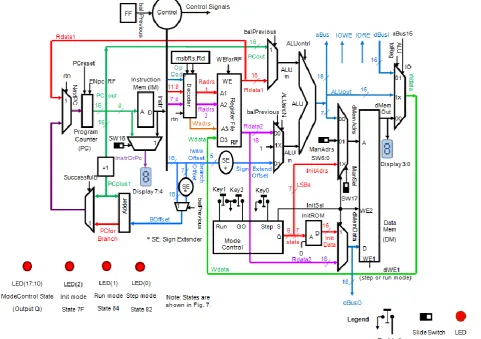
SMaRT enjoys separate data bus and address bus as well. However, each bus is only 16 (not 32) bits wide, as
smaller is faster! SMaRT is a memory-mapped I/O machine with an address space of up to 64 K. See SMaRT datapath in Fig. 1.
SMaRT instructions are single cycle and 16 bits wide with one exception: the branch and link instructions each are 2 words wide and also 2 clock cycles long. The 16x16 register file of SMaRT is orthogonal with one exception: register 1 (R1) is the return address register as explained shortly; otherwise it can be used as a general-purpose register.
In 16-bit-instruction RISC machines with 16 general-purpose registers, it is a challenge to avoid the data loss due to 2-address instructions. To address this shortcoming, we introduce the concept of the so-called
2.5-address machine: SMaRT programmers may specify the register located right after the first operand register as the destination register. For example, the following instruction will add R5 to R2 and place the result in R3, so R2 is not lost anymore:
add+R2, R5
III. SMARTINSTRUCTION SET ARCHITECTURE
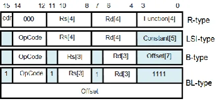
There are four different instruction formats in this machine as shown in Fig. 2, namely R-type, LSI-type, B-type and BL-B-type. Each SMaRT instruction is 16 bits wide (same as the data-bus width) with an exception of baleq and balne to be discussed in this section. The OpCode is always 3 bits wide and occupies bits 12 through 14 of each instruction.
Figure 2. SMaRT instruction formats
A. R-Type Instructions
All the instructions in this category have the same OpCode; the Function field distinguishes between the R-type instructions. In the current (first) version of SMaRT, the following operations are supported: add, sub, and, or, nand, nor, slt. The specified operation is carried out on registers Rs and Rd, and the result goes to register Rd if cdr (MSB of instruction) = 0. See R-type in Fig. 2.
The set less than instruction (slt) compares Rs and Rd, and sets the destination register to 1 if Rs < Rd; otherwise to 0.
Example: slt R3, R6; which means R3 <= 1 if R6 < R3, else 0.
Example: sub R3, R6; which means R3 <= R6 – R3. This, however, may result in a major shortcoming: one of the operand registers, R3 in the above two examples, is overwritten hence lost, which is not something that we like to happen if the overwritten register is going to be used later. We may resolve this issue by adding one more instruction, i.e. spending more time and power, to save the problematic register. Adding one instruction, however,is not an option in this work; we are looking for a less expensive solution to resolve the issue.
A common technique used by processor designers to avoid the data loss is to use 3-address instructions but at a high cost: now the instructions each must be 24 or 32 bits wide as discussed in computer architecture textbooks. But remember smaller is faster!
Example: Use 3-address instruction (not a SMaRT instruction): sub R12, R3, R6; which means R12 <= R6 – R3.
Our novel idea of 2.5-address instructions implemented in SMaRT is able to resolve this issue while the instruction is still 16 bits wide. The cdr bit must be set to 1 to operate in the 2.5-address mode.
Example: sub+R3, R6; which means R4 <= R6 – R3. We frequently need this mode of addressing to avoid the above data loss. The following are two examples to show the need:
Example: In the well-known bubble sort, every two adjacent numbers are read and then swapped if they are not in the right order. Let us use a 2-address instruction to compare the two numbers. We assume that they have already been placed in registers R1 and R2:
slt R2, R1
This way, however, we will lose R2, and therefore not be able to store it at the right address if the numbers happen to be out of order. To resolve this issue we use the following 2.5-address instruction instead:
slt+R2, R1
Example: Suppose that class grades for two tests have been placed in two arrays, and now we are going to write a program to obtain a list of grade pairs each with 10+ points of improvement. In our code, we need to read each grade pair, subtract them, and then compare the difference with 10. Let us say the grade pair is read into R4 and R7. To get the difference if we use instruction sub R4, R7, we will lose R4 and therefore not be able to save it in the output array in case of a satisfactory grade improvement. To resolve this issue, we use the 2.5-address version of sub instead:
sub+R4, R7
Note on 2.5-address instructions: In the current implementation, even if cdr was set to 1, the MSB of the destination register address would not be affected; so Rd: 0111 would create Rd+1: 0000, and Rd: 1111 would result in Rd+1: 1000.
The concept of 2.5-address instructions is the first major contribution of our work in this paper. This way we are able to avoid data loss that inherently exists in 2-address processors. The second major contribution of our work is taking advantage of the temporal locality of reference in accessing the two upper and lower halves of the register file to significantly extend the short-branch range as be explained in Section C.
B. LSI-Type Instructions
There are one arithmetic and two memory reference instructions in this category:
Add Immediate (addi): The 5-bit constant is signed extended and added to Rs; the sum goes to Rd. See LSI- type in Fig. 2.
Load Word (lw): The 5-bit constant is signed extended and added to Rs, the base register, to get the effective address. The word at this address is read from the data memory and placed in Rd. See Fig. 2.
Store Word (sw): The effective address is generated as explained above. Then Rd is written at this address in the data memory. See Fig. 2.
The MSBs of Rs and Rd fields are saved by the R and LSI categories in two flip-flips called msbRs and msbRd, respectively, and then used by the branch instructions that appear after the R or LSI instruction in the SMaRT code as explained shortly.
C. B-Type Instructions
with a range of +/- 64. We also use two special cases to create two more instructions:
Branch on Equal (beq): The 7-bit offset is sign extended and added to PC+1 to get the successful branch address. See B-type in Fig. 2. The next instruction will be taken from this address if Rs = Rd; otherwise the code will continue sequentially.
Note that the Rs and Rd fields are now only 3 bits wide; their MSBs are hidden and will be taken at run time from msbRs and msbRd, the two MSB flip-flops in the CPU. These flip-flops are updated by LSI- and R-type instructions as explained above. This way SMaRT may take advantage of the temporal locality of reference in accessing the two upper and lower halves of the register file. This means that, for example, it is very likely that a branch instruction will use the lower half of the register file if the most recent LSI- or R-type instruction also uses the lower half. Our preliminary studies show a high hit rate for this locality-in-time. As part of our ongoing research, we are looking at different benchmarks to better understand the hit rate. Hiding the two MSBs widens the offset field to 7 bits resulting in a 4-fold increase in the branch range.
Branch on Not Equal (bne): This instruction is similar to the “brach on equal” instruction, but now the branch condition is Rs ≠ Rd.
Set msb FFs and Return from Subroutine: We use the B-type with offset = 0 to create the following two instructions:
Set msb FFs (sff): When the above mentioned temporal locality of reference fails, the programmer may use set msb FFs instruction to explicitly set the MSB flip flops. This instruction stores its bits 10 and 9 in msbRs and msbRd flip-flops, respectively. See Fig. 3. The branch instructions use these MSBs as explained above.
Figure 3. Set msb FFs, a special B-type instruction
Return from Subroutine (rtn): This instruction jumps to the instruction-memory location pointed to by R1. Use this instruction to return from a subroutine.
D. BL-Type Instructions
The range of a short branch instruction is only +/- 64. This constraint is removed in BL-type branches at the cost of one more word (offset) and one more clock cycle. There are 2 instructions in this category, namely baleq
and balne, which additionally save the return address (the word address right after the offset) in register R1. So these instructions are also used to conditionally call subroutines. We have used the short branch instruction formats with an offset of -1 to create the long branches.
Branch and Link on Equal (baleq): The 16-bit offset is added to PC+1 to get the successful branch address. The next instruction will be taken from this address if Rs = Rd; otherwise the code will continue sequentially. In case of a successful branch, the return address will be saved in R1.
The MSBs of Rs and Rd fields will be taken from the MSB flip-flops, which are updated by R-type and LSI-type instructions.
Branch and Link on Not Equal (balne): This instruction is similar to the above instruction, but now the branch condition is Rs ≠ Rd.
E. Input/Output
SMaRT is a memory-mapped I/O processor. The I/O is mapped to the lower half (towards the higher addresses) of the 64-K address space. Therefore, a 1 at the MSB implies an I/O address. SMaRT asserts output lines IORE or IOWE when a lw from an Input Device or a sw to an Output Device, respectively, is being executed. See the SMaRT datapath in Fig. 1.
IV. IMPLEMENTATIONS COSTS
In this section we look at the performance and hardware costs incurred by the above two SMaRT’s novelties. We also show how the control unit takes care of the 2-word 2-cycle long-branch instructions.
A. Cost of 2.5-Address Mode
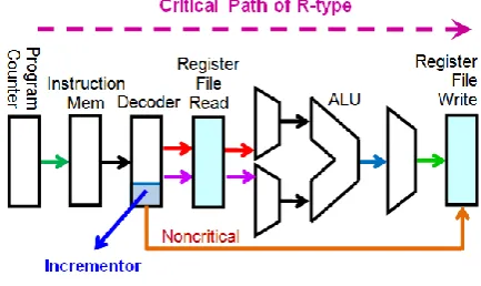
In terms of hardware, the main cost1 for this feature is only one 3-bit incrementor, which takes the 3 LSBs of the Rd field of R-type instructions and generates the 3 LSBs of the destination register address should the cdr bit be set to 1. (The MSB of the destination register address remains unchanged in this process.) In terms of performance, however, no cost is incurred by this novelty as the incrementor is not added to the critical path of the R-type instruction, let alone the critical path of SMaRT. See Fig. 4, where the register file is split into two logical parts, namely “Read Register File” and “Write Register File” to better illustrate the critical path. As you see, the output of the incrementor, the destination register address, will have stabilized well before the output of the ALU stabilizes leaving the incrementor out of the critical path.
Figure 4. Critical path of R-type instructions
The critical path of SMaRT is shown in Fig. 5. In this diagram, the multiplexers are removed to save space. This critical path, which belongs to the lw instruction, is the same as that of the R-type instructions plus the data memory.
1
Figure 5. Critical path of SMaRT
B. Cost of Taking Advantage of Locality of Reference
The major cost components to hide the most significant bits of the register fields in a branch instruction are as follows:
SMaRT uses two flip flops2, msbRs ans msbRd, and logic circuits to set or reset the flip flops by the LSI- and R-type instructions as well as the sff instruction as illustrated in Fig. 6.
Figure 6. MSB FFs: Read and write operations
Flip flop msbRs is loaded with bit 11 of the current instruction if it is LSI or R-type. The flop will be loaded with bit 10 of the current instruction if it happens to be a sff instruction. Similarly, flip flop msbRd is loaded with bit 7 of the current instruction if it is LSI- or R-type. The flop will be loaded with bit 9 of the current instruction if it happens to be a sff instruction. See also Fig. 3.
Fig. 6 additionally shows how the output of the two flip flops are used: If the current instruction is a branch instruction, the MSB of the Rs field will be taken from flip flop msbRs, otherwise from bit 11 of the current instruction. Similarly, if the current instruction happens to be a branch instruction, the MSB of the Rd field will be taken from flip flop msbRd, otherwise from bit 7 of the current instruction. The two flip flops are also shown in Fig. 1 next to the register address decoder.
C. Cost of Long-Branch Instructions
To support the long-branch instructions, SMaRT needs a memory cell in its control unit as shown in Fig. 1. This cell is set to 1 should the current instruction be the first word of a long branch, otherwise it is reset to 0. On the other hand, the memory cell is checked every cycle: if it is set, the current instruction will be interpreted as the
2 We could also use two latches instead of the two flip flops.
offset of the long branch; this will set the program counter to the right jump address if the branch instruction happens to be successful; otherwise SMaRT will skip the offset and continue sequentially.
V. SMARTOPERATION MODES
SMaRT has four operation modes, namely, Single-Step,
Manual, Run and Init. In the Single-Step mode the clock signal is virtually generated by a pushbutton, while the clock frequency is high in the Run mode as well as the Init mode. In the Single-Step mode, you may take SMaRT to the Manual mode in which each data-memory location may be addressed and displayed individually. The output of instruction memory or the output of the program counter may always be selected manually one at a time and displayed. See the SMaRT datapath in Fig. 1. In the Init mode, the contents of a data ROM are copied into the data memory. You may use this mode to initialize the data memory.
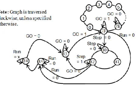
Fig. 7 shows the state machine to control the SMaRT operation modes. There are 3 pushbuttons used in this graph, namely Step, Run and GO. The Step button executes one instruction at a time. The GO button copies the data ROM into the data memory. The Run button executes the program nonstop at a high frequency. In the current implementation, the data ROM is 128 words long. See also the SMaRT datapath in Fig. 1.
Figure 7. SMaRT mode controller
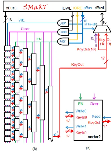
VI. SORTING COPROCESSOR AND PORTS
We first explain a sorting algorithm, then show its 32-key implementation, and finally hook it up to SMaRT, and illustrate the results.
A. Sorting Algorithm
We have used the pipelined and parallel sorting algorithm that we developed in [22] to implement a 32-key bit sorting coprocessor for SMaRT. The 8-32-key 16-bit version of the sorter is depicted in Fig. 8 to better explain how the algorithm works.
is no valid input, the sorting element stays idle. If there is only one valid key, then the sorting element reads and places the key at the output of the element while its valid bit at the output is asserted. If there are two valid inputs, then the sorting element compares them, and places the largest one at the output of the element while its valid bit is asserted. When a valid key is read, its valid bit at the input is deasserted to mark the key as invalid. Invalid keys are grayed out in Fig. 8. The sorting tree will look like Fig. 8b during the second clock cycle. In two more such cycles, the largest key would appear at the root of the sorting tree as shown in Fig. 8d. The other 7 keys will appear at the tree’s root one at a time during the following 7 cycles.
Figure 8. Pipelined 8-leaf sorting tree during 4 clock cycles
B. Implementation
A logic symbol for sorter2, a 2-bit sorting element, is depicted in Fig. 9a. There are 2 input ports for 2 input keys in sorter2. Once sorter2 decides which key to read, it asserts the associated “write” output to mark the selected key as invalid. The selected key is placed at the output of sorter2 along with an asserted valid bit.
We have used thirty one instances of sorter2 organized as a binary tree with 32 leaves to design a 32-key sorter. Fig. 9b illustrates only the upper half of this symmetric tree to save space. A 32-stage shift register is located on the left. The other rectangles are identical instances of sorter2. The way that the sorter is hooked up to SMaRT is also shown in Fig. 9b.
SMaRT is able to write one 16-bit word or key at a time at the tail of the shift register. The tail is mapped to address 8001. So that, a store 8001 instruction will write into the shift register, and additionally will shift the contents of the shift register one location forward. Therefore, the memory bank will fill up after 32 store 8001 instructions. When a word is written at the tail, the valid bit of the tail is set to 1 to indicate a valid key.
Since the sorter’s output is 17 bits wide, the 16-bit key portion and the 1-bit status portion (the MSB) of the sorter’s output are mapped to two different addresses, namely odd and even addresses, respectively. See Fig. 9b. Therefore, a load 8001 instruction will read the “key” output of the sorting tree. Additionally, the same load
instruction will apply one clock pulse to the sorter pipeline, and move it one stage forward. A load 8000 instruction, on the other hand, will only read the status and not move the tree forward anymore. The status word consists of 15 leading 0s followed by the valid bit. Therefore, the status word may be either 1 or 0, which indicates a valid key or an invalid key, respectively.
Once the shift register fills up, SMaRT starts reading and keeps reading the root of the sorting tree until the valid bit is asserted. From now on and with every load 8001 instruction, the valid key at the output of the sorter is read, while the next sorted key replaces the current one.
The port reset address is 8000. So, a store 8000 instruction will reset the system as shown in Fig. 9b. When the sorter is reset, all the valid bits are deasserted.
Figure 9. (a) Sorting element, (b) upper half of sorter
VII. EXAMPLE
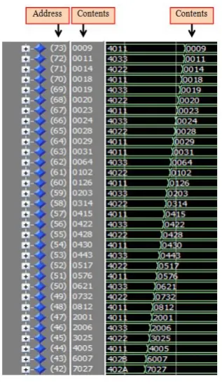
The following SMaRT program sends 32 keys located at data memory addresses 10 through 41 to the sorting coprocessor, waits for the largest number to appear at the root of the sorting tree, and then reads the sorted keys one at a time as they reach the root, and seats them in memory locations 42 through 73:
start: -- machine code
0 sub R0, R0 0x0008 -- reset pointer 1 lw R2, (R0) 0x4020 -- get “reset port”
Adrs 2 addi R1, R2, 1 0x1211 -- get “data port” Adrs 3 sw R2, (R2) 0x5220 -- reset all Valid bits 4 lw R7, 1(R0) 0x4071 --“end of array”
7 sw R6, (R1) 0x5160 -- write it in sorter 8 bne R7, R0, again 0xBF8C -- repeat if not done wait: -- Run sorter and read valid bit until it is set to 1 9 lw R6, (R1) 0x4160 -- run sorter
10 lw R6, (R2) 0x4260 -- read key’s valid bit 11 beq R6, R0, wait 0xAE8D -- do it again if
invalid
--Read sorted keys & put them in dMem until key is invalid: 12 lw R7, 2(R0) 0x4072 --pointer to sorted
array
repeat:
13 lw R6, (R1) 0x4160 -- read key from sorter 14 sw R6, (R7) 0x5760 -- store it in dMem 15 addi R7, R7, 1 0x1771 -- update pointer 16 lw R6, (R2) 0x4260 -- read valid bit 17 bne R6, R0, repeat 0xBE8B -- repeat if valid 18 beq R0, R0, -2 0xA88E -- stay here forever!
Note that this is just an I/O-intensive example to demonstrate the functionality of SMaRT. The performance will be improved should SMaRT communicate with the sorter through a DMA channel. We have implemented a DMA controller for this processor. It is part of our ongoing research to make the most of SMaRT. Fig. 10 shows the simulation result for the above code using the Altera Modelsim simulator.
Figure 10. Simulation results
VIII. CONCLUSION
We presented SMaRT, our small machine for research and teaching, and introduced the novel idea of 2.5-address instructions. This 2.5-addressing mode enables SMaRT to avoid the data loss that exists in 2-address machines, and therefore makes our 16-bit SMaRT
comparable to expensive 3-address 32-bit processors in accessing the register file. In our architecture, the MSBs of the operand registers in LSI- and R-type instructions are carried over to the following conditional branch instructions unless otherwise specified by the programmer. This lets SMaRT’s branch instructions take advantage of the temporal locality of reference in accessing the two upper and lower halves of the register file, and get a significantly larger range by increasing the offset-field width to 7 bits. Based on our preliminary studies we are expecting a high hit rate for this locality-in-time. As part of our ongoing research, we are taking closer look at the hit rate. We then showed that there is almost no performance penalty to achieve these novelties. We also demonstrated that the associated hardware penalty is negligible. To illustrate SMaRT’s functionality, we implemented a sorting accelerator, plugged it into SMaRT, and successfully mapped the whole system into a FPGA chip. The accelerator receives the keys from SMaRT, sorts them and returns them to SMaRT.
SMaRT is our current research platform. The plan is to expand this platform in a variety of directions. To improve SMaRT’s performance, we are now working on a pipelined version of SMaRT. We are also looking at different algorithms and see how efficiently they may be mapped on SMaRT, and therefore how to improve SMaRT to map those algorithms more efficiently. This direction may take us to a SMaRT-based MIMD architecture and open research avenues within the paradigm of Adaptive Network on Chip. Low-power SMaRT is another avenue for our future work towards IOT, the Internet of Things. As the first step in this direction, we are planning to minimize SMaRT’s power consumption at logic level as well as microarchitecture level.
ACKNOWLEDGMENTS
This work was supported by a Topical Grant from KEEN, the Kern Entrepreneurial Engineering Network [23].
REFERENCES
[1] What is a 16 bit microcontroller? Future electronics. [Online]. Available:
https://www.futureelectronics.com/en/Microcontrollers/16-bit-microcontroller.aspx
[2] NXP 8/16 bit MCUs. [Online]. Available:
http://www.nxp.com/products/microcontrollers-and-processors/more-processors/
[3] Microchip 16-bit MCU and DSC programmer’s reference manual.
[Online]. Available:
http://ww1.microchip.com/downloads/en/DeviceDoc/70157F.pdf [4] Texas Instruments MSP430x2xx Family User's Guide. [Online].
Available: http://www.ti.com/lit/ug/slau144j/slau144j.pdf [5] S. Barrett and D. Pack, Microcontroller Programming and
Interfacing: Texas Instruments MSP430, 1st ed., Morgan &
Claypool Publishers, 2011.
[6] H. W. Huang, The HCS12 / 9S12: An Introduction to Software and Hardware Interfacing, 2nd ed., Delmar Cengage Learning, 2009.
[7] L. D. Jasio, Programming 16-Bit PIC Microcontrollers in C Learning to Fly the PIC 24, 2nd ed., Newnes, 2011.
[8] T. Wilmshurst, Designing Embedded Systems with PIC Microcontrollers: Principles and Applications, 2nd ed., Newnes,
[9] Dragon12-Plus-USB trainer for Freescale HCS12 microcontroller family user’s manual for Rev. G board, Revision 1.10. [Online]. Available:
http://www.evbplus.com/download_hcs12/dragon12_plus_usb_9s 12_manual.pdf
[10] Microchip explorer 16 development board user’s guide. [Online]. Available:
http://ww1.microchip.com/downloads/en/DeviceDoc/Explorer%2 016%20User%20Guide%2051589a.pdf
[11] Microchip PIC32MX family reference manual. [Online]. Available:
http://hades.mech.northwestern.edu/images/2/21/61132B_PIC32R eferenceManual.pdf
[12] D. A. Patterson and D. R. Ditzel, “The case for the reduced instruction set computer,” ACM SIGARCH Computer Architecture News, vol. 8, no. 6, pp. 25-33, 1980.
[13] ARM’s Reach: 50 billion chip milestone. [Online]. Available: http://www.broadcom.com/blog/chip-design/arms-reach-50-billion-chip-milestone-video/
[14] F. C. Yang and I. J. Huang, “An embedded low power/cost 16-bit data/instruction microprocessor compatible with ARM7 software tools,” in Proc. Asia and South Pacific Design Automation Conf., Yokohama, 2007, pp. 902-907.
[15] S. M. S. Muslim and Z. U. Ahmad, “Design of an algorithmic state machine controlled, field programmable gate array based 16-bit microprocessor,” in Proc. Intl Symposium on Integrated Circuits, Singapore, 2007, pp. 434-436.
[16] L. Morales-Velazquez, R. A. Osornio-Rios and R. J. Romero-Troncoso, “FPGA embedded single-cycle 16-bit microprocessor and tools,” in Proc. IEEE Intl Conf. on Reconfigurable Computing and FPGAs, Cancun, 2012, pp. 1-6.
[17] A. S. Gheorghe and C. Burileanu, “Savage16 - 16-bit RISC architecture general purpose microprocessor,” in Proc. Intl Semiconductor Conf., Sinaia, 2010, pp. 521-524.
[18] S. Sakthikumaran, S. Salivahanan, and V. S. K. Bhaaskaran, “16-Bit RISC processor design for convolution application,” in Proc. Intl Conf. on Recent Trends in Information Technology, Chennai, 2011, pp. 394-397.
[19] J. L. L. Presa and E. P. Calle, “MMP16 a 16-bit didactic micro-programmed micro-processor,” in Proc. International Conf. on Computer Research and Development, Shanghai, 2011, pp. 61-65. [20] T. C. Tang, L. Kung, C. C. Ho, and H. J. Chang, “Embedded
controller design for portable fuel cell,” in Proc. 9th
Intl Conf. on Information, Communications and Signal Processing, Tainan, 2013, pp. 1-3.
[21] A. Suwannakom, “Adaptive control performance of a mobile robot using hybrid of SLAM and fuzzy logic control in indoor environment,” in Proc. Intl Electrical Engineering Congress, Chonburi, 2014, pp. 1-4.
[22] N. Tabrizi and N. Bagherzadeh, “An ASIC design and formal analysis of a novel pipelined and parallel sorting accelerator,” Integration, the VLSI Journal, vol. 41, no. 1, pp. 65-75, 2008. [23] The Kern Family Foundation. [Online]. Available:
http://www.kffdn.org/entrepreneurial-mindset/
Dr. Nozar Tabrizi received his BS and MS