Advanced design and characterization methodologies for
memory-aware CMOS power-amplifier implementation
Martin Schleyer, Dominic Maurath, Heinrich Klar, and Friedel Gerfers
Department Mixed Signal Circuit Design, Faculty IV, Technical University Berlin, 10587 Berlin, Germany
Correspondence to:Dominic Maurath ([email protected])
Received: 21 December 2016 – Revised: 13 April 2017 – Accepted: 22 April 2017 – Published: 21 September 2017
Abstract.This paper reports on an effective root-cause anal-ysis method of memory effects in power amplifiers, as well as introduces compensation techniques on a circuit design level. Despite conventional memory-effect approaches, the discussed method uses a two-tone scan over a wide op-eration and modulation range. This enables an in-depth study of physical causes and helps to implement compen-sation techniques at design stage. On the one hand, this circuit investigation is optimized using an automated Sys-temC model parametrized with real device and measurement values. Hence, computation time is widely reduced which shortens design cycles. On the other hand, the implemen-tation of the derived circuit compensation means will duce the complexity of digital pdistortion due to a re-duced memory-effect inre-duced AM/AM and AM/PM hystere-sis. The approach is demonstrated on a 65 nm CMOS power amplifier with an OIP1 of 27 dBm and a PAE of over 30 % using WCDMA and LTE signals. In fact, mismatch could be reduced by more than 8 %.
1 Introduction
A common approach in radio transmitter design is using digital pre-distortion (DPD) and linearization in order to deal with power amplifier induced linearity. These non-linearities are usually a function of signal power and fre-quency. Since such effects are very deterministic, DPD can be used with high reliability. However, as real transmitter systems are actually more complex the signal history has ap-peared as an important measure for signal distortion (Bösch et al., 1989). This is addressed/concluded as the memory ef-fect of power amplifiers, and is non-deterministic (no (quasi) steady state available) due to the unknown signal history
at design time (Martens et al., 2012). That is, while distor-tion caused by regular non-linearity (frequency, amplitude) is much easier to be compensated, non-linearity induced by memory effects inflate DPD efforts, causing significant pro-cessing overhead, and reduce the reliability of RF signal fi-delity (Brunk et al., 2011). That is, in non-linear circuits there are intermodulation products near the location of the actual modulation frequencies and its harmonics (Vuolevi et al., 2000). In case of further non-linear processes the impedances of the source, load, and the amplifier itself become more important as the modulation frequencies are mixed into the band of the fundamental frequency.
As the need for higher data rates and spectrum efficien-cies continuously rises, so is the need for RF signal linearity. Higher-order modulation schemes only allow a small error vector magnitude, and thus, any amplitude or phase error di-rectly degrades possible data rate, i.e. increases the bit-error rate (BER). Further on, power amplifier memory effects usu-ally causes asymmetric sidebands in the frequency spectrum, which is problematic for the needed compliance to adjacent channel power ratio specifications (e.g.−60 dBm) – hence, the maximum output power of the radio transmitter need to be artificially reduced.
Figure 2.Evaluation of the time-domain measurement withPin=22 dBm and 10 MHz two-tone spacing.
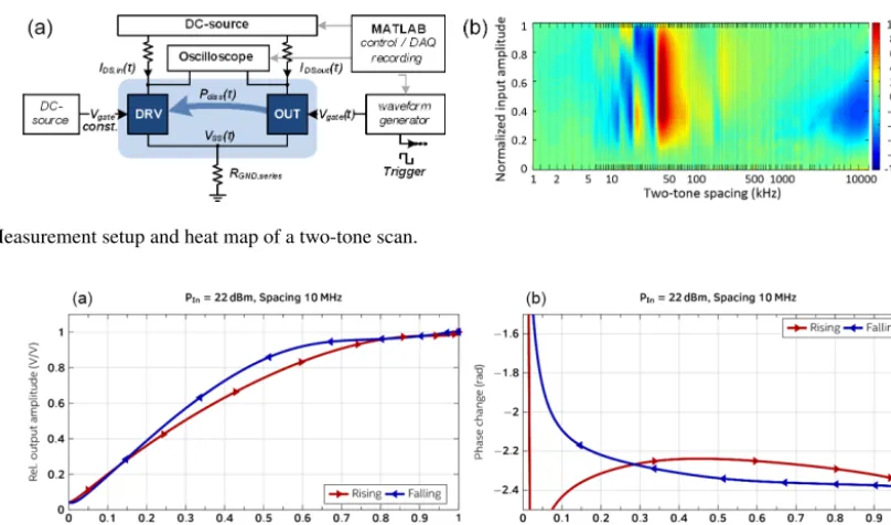
In general, there are short-term, and long-term memory ef-fects. Both have different physical root-causes as suggested in Wolf et al. (2010). Short-term effects are referred to as electrical effects (inductive behavior) usually caused by fre-quency depend impedances of the source, the load, and the amplifier itself. This is particular significant for narrowband matching networks. The long-term effects are caused by ther-mal processes due to therther-mal conductance and therther-mal ca-pacitance (e.g. due to self-heating) Hence, transferring these electrical and thermal effects into a system design context, there are additional poles and zeros due to the memory ef-fect. Figure 1b provides a heatmap recorded with the two-tone setup. While the left-handed areas refer to thermal ef-fects (long-term, capacitive poles), the further right-hand side areas refer to a larger envelop frequency, thus, indicating memory effects related to electrical causes (short-term, in-ductive zeros). The red to blue color range indicates positive and negative distortions of the AM/AM time-domain trajec-tories. The sudden phase change at about 35 kHz two-tone spacing indicates a thermal pole. As usually multi-stage am-plifiers are used, there is a critical issue if the thermal cou-pling between individual amplifier stages create additional feedback loops which interact with the designed and imple-mented electrical feedback loops. That is, in conjunction with such thermal poles, the phase margin deteriorates, and the power amplifier could even enter instability, i.e. resonance states. Thus, causes signal loss, as well as device stress and operation failure.
Figure 2 shows a concrete sample of the heatmap scan. For better distinction, the plots use a blue line for ascending amplitudes, and a red line for decreasing amplitudes. More
specifically, it can be concluded that the influence of the ther-mal RC network on AM/AM results for higher temperatures are that there is (i) less gain, and (ii) a frequency shift due to capacitive behavior. This is also clearly visible in the model as well as measurements. The relation of the time constants and hysteresis, is that there is for low frequencies also a low hysteresis, but no hysteresis for high frequencies. Further-more, the simulation shows a strong hysteresis around corner frequency.
2 Modelling, parameter extraction and design flow
Figure 3.Detailed SystemC/AMS block level modelling for the parameter extraction.
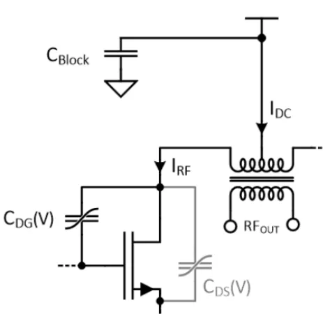
Figure 4.Band pass effect of the drain bias node.
2.1 Root-cause analysis
Using the proposed measurement concept the memory ef-fect is scanned (measured and quantified) over envelop fre-quency (two tone spacing) and input amplitude variation. As compared to other measurement approaches which only fo-cus on certain inter-modulation products (IMDs), the two-tone method does not suffer from information loss. This is possible because the efficient modelling approach allows a full scan of a wide two-tone range, as well as for the full amplitude range in an affordable time and computa-tion power. However, the measurement is significantly more effort. Therefore, an appropriate concept is introduced, to shorten the characterization procedure, as shown in Figs. 1 and 3. A detailed introduction into the automation and model
Figure 5.Memory-aware design concept.
verification is given in Schleyer et al. (2014). The algo-rithm processes the AM/AM and AM/PM time-domain tra-jectories, and applies calibration with chirp-signals (Wolf et al., 2009). The design framework is optimized for electro-thermal co-design. By transferring the electro-thermal behavior into an equivalent electrical model (RC approach, thermal co-evaluation), also electrical evaluation methods of circuit sim-ulators are useable.
2.2 Thermo-induced operating point effects
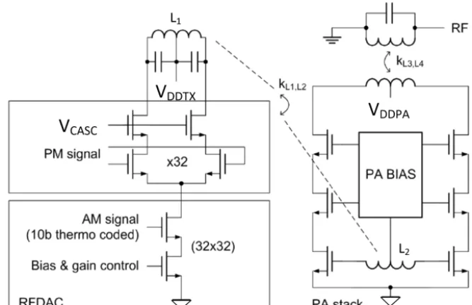
Figure 6.Connection of RFDAC and an integrated PA.
Figure 7.Stacked cascode circuit with dynamic biasing.
2.3 Specification driven design methodology
Figure 5 concludes the electro-thermal effects, and maps them to modelling as well as implementation concepts. A memory aware design certainly relies on the designer’s ex-perience, but coordinating the root-cause and design options in a structured and quantifiable manner inevitable for good performance results. As system specifications tend to higher carrier frequencies, as well as a high integration density, low
Q-factors of passive components as well as the thermal inter-action, e.g. in flip-chip packages, add design complexity and need to be optimized. In addition, appropriate biasing
con-cepts, multi-stage feedback structures, and impedance trans-formation networks need to be optimized, as well as the bandwidth limitation to be understood.
Memory-aware specification allow more effective and re-liable designs.
3 Design example: dynamic biasing in CMOS RF power amplifiers
Based on the root-cause analysis provided above, this sec-tion discusses two successful design approaches to compen-sate memory effects in power amplifiers. The discussion here focuses on the output stage of power amplifiers as they trans-form most power into heat.
3.1 Connection of RFDAC and integrated PA
In order to compensate for the thermally inducedCDS and bias point modulation the gate biasing needs to be adapted accordingly. A possible implementation is presented in Fig. 6 (Moreira et al., 2015). A RF digital-to-analog converter (RF-DAC) is used to generate bias and gain control as well as an AM signal. In addition, a differential PM signal improves the dynamic bias tracking for reduced memory effect. Even-tually the bias setting is RF-coupled to the power amplifier gate biasing circuit. The advantage of this approach is that the drain node of the PA transistors is at a constant level that implies zero drain impedance. Thus, the gain is only reduced by compression, but not by memory effects. Hence, also the baseband spectrum is improved.
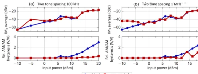
mit-Figure 8.Improvement due to the compensation of memory effects. Flattening of the AM/AM line indicates the reduced dependency on the input signal amplitude (OIP1 equals 27 dBm, with a PAE of over 30 %).
igate device voltage stress. Due to this additional transistors, the design needs to be carefully optimized in order achieve a good trade-off between robustness to voltage stress and effi-ciency.
3.2 Dynamic gate modulation (concept of VG2 modulation)
Another design approach is to modulate the complete tran-sistor well with a dynamic biasing, as illustrated in Fig. 7. A successful implementation of this approach is discussed in Leuschner et al. (2010) and Leuschner et al. (2011). The baseband impedanceZBBis seen from the cascade load tran-sistor into VDD nodes. The drain impedance ZM1 is seen from M1into cascade. Thereby, the assumption is that the impedance ZM1 influences linearity and memory. There-fore, for large RF signals, the power amplifier goes into class-B operation, and the drain node of M1 sees a vary-ing impedance and thus the AM/AM and AM/PM behav-ior is altered. Hence, two direct implications are to avoid a phase shift between drain voltage and current, which can be achieved by a real-valuedZbias. Moreover, the termination of baseband (BB) components with a short circuit will reduce theVdrain,BBcomponent. The positive effect is a reduced PM hysteresis due toCDS(Vdrain,BB),and also a reduced AM hys-teresis due to up-mixing ofVdrain,BB.
The stacked cascode approach has different degrees of freedom. First, the bias network limited to one inductive el-ement (transformer), second, the drain resistance seen from input transistorM1can be varied via the additional gate bias node. Third, overcompensation helps the correction of IM2 contribution. In addition, the overall IM3 can be real valued and hence symmetric.
4 Performance results
Applying the aforementioned design options from Sect. 3 to-gether with the analysis methodology discussed in Sect. 2 allows already at design time the quantification of
perfor-mance improvements. This is important for the system design as early insights are available regarding the need for or avoid-ance of additional digital linearization and pre-distortion measures.
In order to evaluate the performance improvement, a two-tone excitation in the range of 100 kHz and 1 MHz is per-formed. The objective is the flattening of the AM/AM line as a result of the minimization of the dependency on input sig-nal amplitude. As shown in Fig. 8, using dynamic bias point modulation and baseband injection can significantly reduce memory effects, which is visible by the reduced opening of graphs for compensated operation. Hence, using a stan-dard peak-to-average-power-ratio (WCDMA), the improve-ment of AM/AM mismatch can be over 8 % in average.
5 Conclusions
The root-cause analysis and design conclusions presented in this paper are shown to be relevant for future high-performance power amplifiers in radio front-ends. Analyz-ing and understandAnalyz-ing the root-cause of the memory-effects and mapping them to design methodology leads to significant improvement, while additional complexity in the digital do-main is avoided. Starting from an electro-thermal co-design approach with automated measurement setup, the electrical on operating point and parasitic device capacitances can be linked to the circuit behavior. The development of dynamic compensation methods revealed a stacked-cascode approach as well as a modulated-well technique as two potential candi-dates for the compensation of memory-effect by analog cir-cuit design.
Data availability. Proprietary channel model from company was used and is not publicly available.
on Microwave Theory and Techniques, 37.12, 1885–1890, https://doi.org/10.1109/22.44098, 1989.
Brunk, M. and Jüngel, A.: Self-heating in a coupled thermo-electric circuit-device model, J. Comput. Electron., 10, 163–178 https://doi.org/10.1007/s10825-010-0324-9, 2011.
Leuschner, S., Pinarello, S., Hodel, U., Mueller, J. E., and Klar, H.: A 31-dBm, high ruggedness power amplifier in 65-nm standard CMOS with high-efficiency stacked-cascode stages, in: Radio Frequency Integrated Circuits Symposium (RFIC), IEEE, 395– 398, https://doi.org/10.1109/RFIC.2010.5477401, 2010. Leuschner, S., Mueller, J.-E., and Klar, H.: A 1.8GHz wideband
stacked-cascode CMOS power amplifier for WCDMA applica-tions in 65 nm standard CMOS, in: Radio Frequency Integrated Circuits Symposium (RFIC), IEEE, 1–4, 2011.
https://doi.org/10.5194/ars-12-95-2014, 2014.
Wolf, N., Mueller, J.-E., and Klar, H.: Identification of frequency dependent memory effects and the lineariza-tion of a CMOS PA for multiple standards, in: Ra-dio and Wireless Symposium (RWS), IEEE, 598–601, https://doi.org/10.1109/RWS.2009.4957422, 2009.
Wolf, N., Müller, J.-E., and Klar, H.: Simple pre-distortion system for compensation of temperature dependent nonlinearity of power amplifiers, in: Radio and Wireless Symposium (RWS), IEEE, 152–155, https://doi.org/10.1109/RWS.2010.5434250, 2010.