T E C H N I C A L N O T E
Open Access
Development of SEM and STEM-in-SEM
grid holders for EDS analysis and their
applications to apatite phases
Yong-Eun Kwon
1,2, Jung-Kyun Kim
3, Yong-ju Kim
4, Jin-Gyu Kim
2*and Youn-Joong Kim
1,2*Abstract
Background:With the application of the scanning transmission electron microscopy (STEM) detector, transmitted electron images similar to transmission electron microscopy (TEM) can be obtained from scanning electron microscopy (SEM), which is referred to STEM-in-SEM imaging. Compared to TEM-energy dispersive spectroscopy (EDS), SEM-EDS is expected to be more efficient and reliable for chemical analysis of TEM specimens due to the larger sample space in SEM and the higher take-off angle of the SEM-EDS detector. Unfortunately, this advantage is not well applied to TEM specimens in practice, mainly because of fault signals generated from the commercial grid holders used in SEM and STEM-in-SEM. This study is designed to solve this problem by modifying the commercial holders and to test them through EDS analysis of apatite phases.
Findings:We first changed the way of assembling parts of the commercial multi-grid holder for SEM. This new assembly was capable of producing a thinner upper cover part, resulting in the reduction of the EDS fault signals generated from the holder. Furthermore, the thin upper part allowed us to get images in shorter working distances, that is, at higher magnifications. This design concept was also applied to the commercial single-grid holder for STEM-in-SEM, producing a new multi-grid holder to be used for loading multiple samples.
Conclusion:We confirmed that the new holders produced reliable chemical data from apatite phases. In case of
oxygen analysis, despite of low electron brightness from the tungsten source, 5 kV provided more stable acquisition and signal yields than 15 kV. We expect that these modified holders facilitate more efficient EDS analysis for multiple samples under the same analytical conditions in SEM and STEM-in-SEM.
Keywords:SEM, STEM-in-SEM, EDS, TEM specimen, Multi-grid holders, Apatite phases
Introduction
Through the advance of electron microscopy, structural and chemical information of various materials can be routinely obtained at the nanometer scale. Detectors have been continuously developed for collecting a range of specific electronic signals generated from the sample. Among them, the detector for scanning transmission electron microscopy (STEM) can produce high contrast images due to its selective detection of transmitted elec-trons. Moreover, the STEM detector is not just applied to transmission electron microscopy (TEM), but can be
utilized in scanning electron microscopy (SEM) as well. In case of STEM study in SEM, referred to as STEM-in-SEM, the STEM detector can select specific diffraction angles or directions of the transmitted electrons by adjusting various apertures and detector positions owing to its large detecting area (Probst et al., 2007; Beyer et al.,2012; Hondow et al.,2012; Holm & Keller,2016).
As STEM-in-SEM uses low accelerating voltages usu-ally below 30 kV, it has an advantage of producing high-contrast images from samples which could be vulnerable to electron beam damage such as polymers and biomate-rials (Guise et al., 2011; Garcia-Negrete et al., 2015). In addition, STEM-in-SEM is capable of loading multiple TEM grids, which makes it easier to conduct analysis under consistent analytical conditions without sample exchange. Since SEM and STEM images can be obtained
© The Author(s). 2019Open AccessThis article is distributed under the terms of the Creative Commons Attribution 4.0 International License (http://creativecommons.org/licenses/by/4.0/), which permits unrestricted use, distribution, and reproduction in any medium, provided you give appropriate credit to the original author(s) and the source, provide a link to the Creative Commons license, and indicate if changes were made.
* Correspondence:[email protected];[email protected]
2Korea Basic Science Institute, Daejeon 34133, Republic of Korea
1Graduate School of Analytical Science and Technology, Chungnam National
University, Daejeon 34134, Republic of Korea
simultaneously, STEM-in-SEM can provide us morpho-logical three-dimensional information, rather than pro-jected two-dimensional information from the TEM specimen (Probst et al.,2007; Beyer et al.,2012).
Although a large number of studies have been car-ried out utilizing STEM-in-SEM, such studies do not emphasize the advantages of SEM-energy dispersive spectroscopy (EDS) for chemical analysis. Because the SEM-EDS detector is typically installed with higher take-off angles compared to the TEM-EDS detector, it does not require specimen tilting during analysis, which is favorable for stable signal acquisition. Fur-thermore, flexible accelerating voltage settings to low voltages such as 5 kV are useful to find suitable ana-lytical conditions considering the ionization yields of light elements to be analyzed (Wu et al., 2015; Wil-liams & Carter, 2009; Goldstein et al., 2018).
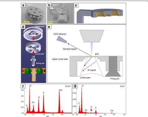
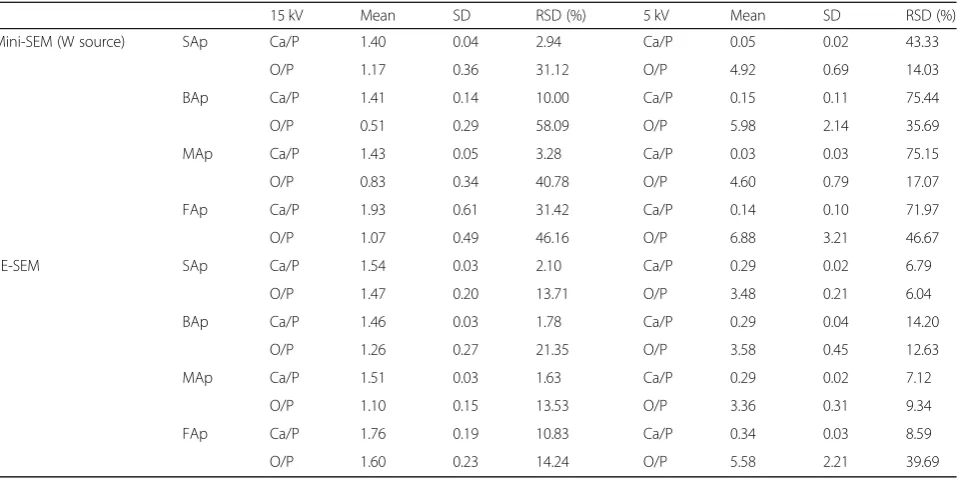
However, due to the spacious SEM chamber with lots of accessories inside and the large size of the sample holder itself, unwanted EDS signals could be generated from other sources than the actual sample to be ana-lyzed. The commercial SEM grid holder, used for load-ing four TEM grids, actually produced unwanted Al signals during the test session (Fig. 1). To mitigate this problem, we modified the commercial grid holder to re-duce the fault signals. Additionally, a new grid holder for STEM-in-SEM was designed to load four separate TEM grids instead of the commercial single-grid holder. We designated the modified holders as multi-grid holders of type 1 for SEM and type 2 for STEM-in-SEM in our de-scription (Fig.2).
Using the modified multi-grid holders, we have carried out EDS analysis of four types of apatite phases at 15 kV and 5 kV. Each EDS spectrum was obtained at a single
session in consistent analytical conditions, and intensity ratios of Ca/P and O/P were interpreted. Through com-parative analysis of apatite phases with both pure and mixed chemistry, we were able to distinguish specific chemical characteristics of the four apatite phases which have similar chemistry (Lee et al.,2013; Kim et al.,2018).
Experimental
For this study, two types of commercial grid holders were used, a multi-grid holder for SEM (catalog #75949-03, EMS) and a single-grid holder for STEM-in-SEM (COXEM). These holders were modified to be suitable for EDS analysis. To test the commercial and modified grid holders, we used two types of SEM instruments, a table-top tungsten filament SEM (Mini-SEM, EM-30SX, COXEM) operating at 1~30 kV, and a normal field emis-sion SEM (FE-SEM, Merlin, Carl Zeiss, installed at the
Korea Basic Science Institute) operating at 0.02~30 kV. The Mini-SEM was equipped with a Mini-EDS detector (Elements, EDAX: take-off angle 24.37°; detector area 15 mm3), and the FE-SEM was equipped with a normal EDS detector (XFlash 6l60, Bruker: take-off angle 35°; detector area 60 mm3).
Limitations of the commercial grid holders
Figure 1a and d display the commercial multi-grid holder and COXEM single-grid holder. As shown in Fig.1b and e, these holders were manufactured for SEM and STEM-in-SEM imaging only, without considering EDS analysis, and had thick upper cover parts. Since the thick cover obscured sample signals and generated Al signals, we obtained EDS spectra having dominantly Al intensities originated from the holder material as shown in Fig. 1g and h. Although synthetic hydroxyapatite
Fig. 2aThe modified multi-grid holder (type 1) for SEM.bThe modified multi-grid holder (type 2) for STEM-in-SEM.cThe cross-section image of
(SAp, Ca5(PO4)3OH, 574791-15G, Sigma-Aldrich) was examined at 15 kV, the spectra did not show noticeable Ca and P peaks, which are major constituting elements of apatite. We presumed these shortcomings originated from how the holder was assembled. That is, the com-mercial holders were designed to support the cover from above by the fixing screw. As shown in Fig.1i, the fixing pin is a type of flat-head cap screw, and the screw head presses the upper cover for support. Therefore, the upper cover requires a thickness level compatible with the screw head. The thick cover generated strong Al sig-nals which were a major obstacle to the genuine sample signals. Finally, we arrived at the conclusion that it was important to minimize the holder regions which may potentially generate the fault signals for proper EDS ana-lysis on the TEM specimen.
Developing modified multi-grid holders
On the purpose of directing EDS signals into the de-tector and loading multiple samples, we modified the commercial grid holders. Figure 2a and b show the modified multi-grid holders of type 1 and type 2, re-spectively. In order to minimize interaction between the upper cover part region and the signal, we changed the assembling way of the grid holder. The new assembly supported the holder in such a way that the fixing pin pushed the lower part from below, which allowed the screw head to be hidden underneath, and the upper cover to be much thinner. Figure 2d shows how to as-semble parts of the type 1 holder by the fixing pin. In addition, we processed the lower part in concave form to minimize the interaction with the transmitted elec-trons. The schematic diagram in Fig. 2e illustrates that the thin cover does not block EDS signals from the sam-ple to the detector. We confirmed that EDS analysis using the modified holders detected Ca, P, and O peaks of SAp as shown in Fig. 2f and g. Because the modified holders were designed to load four separate samples, we can perform EDS analysis in consistent conditions with multiple samples both in SEM and in STEM-in-SEM. In addition, the thinner upper part allowed us to carry out SEM and light microscopy (LM) in shorter working dis-tances, thus, at higher magnifications. Since the type 1 holder is adaptable to any SEM instruments which use the pin-type stub, we can evaluate performances of SEM-EDS systems of interest using the same standard materials. On the other hand, the type 2 holder is cur-rently dedicated to the Mini-SEM attached with the STEM detector. We can carry out STEM imaging and EDS analysis at the same time with this holder.
Application of the modified holders to multiple samples
Both synthetic and natural apatite samples (Kim et al.,
2018; Song et al.,2012; Meneghini et al.,2003; Young et al.,
1969; Kim et al.,2017) were used to test the efficacy of the modified holder for STEM-in-SEM EDS analysis. While commercial SAp was available in powder form, mineral apatite (MAp, 470104-508, Ward’s Science) and fossil apatite (FAp, left femur from a Cretaceous dinosaur (Kim et al.,2017)) required powdering via diamond sawing (deb-ris collection), ultrasonic drilling, and/or were ground with an agate mortar and pestle in order to avoid chemical and structural alterations. In case of bone apatite (BAp), aiming to retain its original state, we avoided using chemical agents that were involved in decalcification and fixation (Kim et al.,2018). The bone sections were cut using a diamond wire saw (Model 3242, Well), were subsequently dried in a crit-ical point dryer (Samdri®-PVT-3D, Tousimis) for an hour, and were finally powdered using a freezer mill (SPEX Sam-ple Prep™). The collected BAp was added to a 70% ethanol solution (Kim et al., 2018). All the other apatite samples were added into 99.9% ethanol solutions, and the solutions were stored in room temperature. The nanoparticles within each sample solution were separated into individual parti-cles by a probe sonicator (EpiShear, Active Motif). We sprayed each sample solution onto each TEM grid using the custom-made ultrasonic sprayer to prevent aggregation between particles as well as to disperse the sample particles widely enough during the drying of the solution on the grid (Kim et al.,2018).
For comparison, we tested the same samples with a Zeiss grid holder (12x STEM-probenhalter) for the FE-SEM, which is manufactured by Carl Zeiss, but covered with a custom-made Be plate to avoid generation of Al signals. Four TEM specimens were analyzed at the same analytical conditions. Forty spectra per each sample from each instrument were acquired at both 15 kV and 5 kV, considering the ionization yields of Ca and O (Wu et al.,
2015; Williams & Carter, 2009; Goldstein et al., 2018; Newbury & Ritchie, 2013). Although the image quality was somewhat poor in case of 5 kV using the Mini-SEM, we adjusted the condenser lens to increase the electron dose. Each spectrum in all samples was collected for 100 s from the 500 × 500 nm region. To compare the ra-tio of Ca and O to P, we calculated the Ca/P and O/P ratio using the spectra obtained at 15 kV and 5 kV. Data analysis and configuration were done with the EDAX software TEAM for the Mini-SEM and the Bruker soft-ware ESPRIT 2.0.0 for the FE-SEM.
Results and discussion
EDS analysis of apatite phases
was higher at 5 kV due to the low ionization energy of oxygen (Wu et al.,2015; Williams & Carter,2009; Gold-stein et al.,2018). Relative standard deviations (RSD) in-dicated that statistical data reliability of each element was affected by accelerating voltages selected.
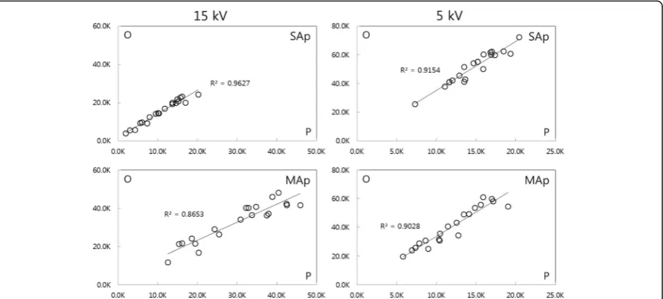
In order to interpret the EDS results more quantita-tively, we plotted the data on the correlation graphs of Ca and P. Figure 3 shows correlation graphs of four types of apatite. Although each intensity value is not constant due to the irregular population of sample parti-cles from the analyzed area, the correlation graphs of Ca and P show good proportionality, and the trend lines represent the characteristics of each apatite phase. The graphs of SAp and MAp in Fig. 3 have constant and straight trend lines as they are reference materials with high chemical purity, in contrast to those of BAp and FAp. Since the slopes represent Ca/P of each apatite, we notice that Ca/P of BAp is lower than those of SAp and MAp. However, the data points of BAp show larger devi-ation from the trend line, which suggests that the chem-istry of BAp maybe not homogeneous possibly due to material exchange (LeGeros et al., 2009; Fleet et al.,
2004). In case of FAp, the Ca/P value listed in Table 1
has an abnormally high mean value, suggesting the pres-ence of Ca-rich minerals other than FAp, such as calcite (CaCO3). For this reason, it is difficult to find the true Ca/P of FAp by using the calculated mean values only. On the other hand, the graph of FAp in Fig. 3 clearly shows the trend line as well as points deviating from the trend line originating from Ca-rich minerals. This ana-lytical method, comparing unknown materials with the
reference materials using our multi-grid holders, is quite useful for the analyses of inhomogeneous samples like BAp and mixed samples with other impurities like FAp. It is also noticed that the statistical processing using a large amount of EDS data is very important for reliable chemical analysis of materials through SEM and STEM-in-SEM.
Comparison of EDS data for oxygen
As shown in Fig. 4, the EDS data of the Mini-SEM using the reference materials indicated that the reli-ability of O/P was improved at 5 kV compared to the data at 15 kV. Although the total intensity was de-creased at 5 kV, the distributions of data changed from sporadic to linear, which was reflected in higher R2
(coefficient of determination) values. However, these values were insufficient to do reliable chemical analysis on light elements, comparing to the data ob-tained by the FE-SEM, as shown in Fig. 5. In case of the Mini-SEM, it is estimated that some oxygen sig-nals were absorbed by the geometry of particle sur-faces due to the low electron penetration depth at 5 kV, resulting in insufficient signals (Wu et al., 2015; Goldstein et al., 2018; Newbury & Ritchie, 2013).
By comparison, the FE-SEM, besides the field emission source, uses a special electron optical column technology which is called“integrated beam-accelerator,”to achieve high resolution and brightness even at the lowest accel-erating voltages (Jaksch & Martin, 1995). Because the FE-SEM is able to reduce the loss of electrons moving from the gun to the sample by “cross-over-free-mode”
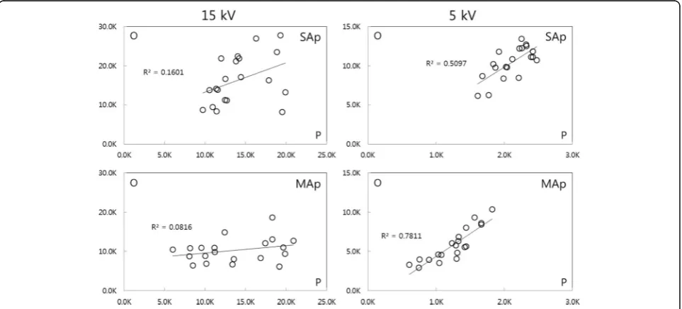
Table 1Intensity ratios of Ca and O to P at 15 and 5 kV from the Mini-SEM and FE-SEM. (Mean, SD = standard deviation. RSD = relative standard deviation (SD/Mean × 100(%))
15 kV Mean SD RSD (%) 5 kV Mean SD RSD (%)
Mini-SEM (W source) SAp Ca/P 1.40 0.04 2.94 Ca/P 0.05 0.02 43.33
O/P 1.17 0.36 31.12 O/P 4.92 0.69 14.03
BAp Ca/P 1.41 0.14 10.00 Ca/P 0.15 0.11 75.44
O/P 0.51 0.29 58.09 O/P 5.98 2.14 35.69
MAp Ca/P 1.43 0.05 3.28 Ca/P 0.03 0.03 75.15
O/P 0.83 0.34 40.78 O/P 4.60 0.79 17.07
FAp Ca/P 1.93 0.61 31.42 Ca/P 0.14 0.10 71.97
O/P 1.07 0.49 46.16 O/P 6.88 3.21 46.67
FE-SEM SAp Ca/P 1.54 0.03 2.10 Ca/P 0.29 0.02 6.79
O/P 1.47 0.20 13.71 O/P 3.48 0.21 6.04
BAp Ca/P 1.46 0.03 1.78 Ca/P 0.29 0.04 14.20
O/P 1.26 0.27 21.35 O/P 3.58 0.45 12.63
MAp Ca/P 1.51 0.03 1.63 Ca/P 0.29 0.02 7.12
O/P 1.10 0.15 13.53 O/P 3.36 0.31 9.34
FAp Ca/P 1.76 0.19 10.83 Ca/P 0.34 0.03 8.59
and “beam-accelerator-mode,” it is possible to obtain high electron density, that is, high signals in EDS ana-lysis at low kV (Jaksch & Martin, 1995). In Fig. 5, the graphs show that the FE-SEM obtains sufficient intensity of O and P even at 5 kV, resulting in statistically reliable data with high R2. On the other hand, the Mini-SEM, with the tungsten filament and only minimal electron optical column configuration within the small space, is easily exposed to the analytical limitation at low voltages where the amount of electrons is not sufficient.
Since low-voltage EDS is useful to achieve high-reso-lution chemical mapping and to obtain efficient chemical spectra in low ionization energy ranges, its demand is in-creasing in the fields of surface analysis and light element analysis (Burgess et al.,2017). In this study, we confirmed that the electron source is very important for signal acqui-sition. In the Mini-SEM, if the electron source is replaced with other sources of higher brightness, we will have higher signal acquisition and more reliable EDS analysis, in addition to higher resolution in imaging due to the
Fig. 3Correlation of the Ca and P intensities for apatite phases obtained at 15 kV using the Mini-SEM. The data of the reference materials, SAp and MAp, show constant and straight lines. The slope of the trend line from BAp indicates lower Ca/P compared to SAp and MAp. FAp shows certain data points distributed outside the line, which suggests the presence of Ca-rich minerals other than apatite, such as calcite (CaCO3)
smaller crossover size (Williams & Carter,2009). Through improvement of additional parts such as power supplies affecting the stability of voltage and current, we expect that the Mini-SEM could become a better analytical and imaging tool with the multi-grid holder for SEM and STEM-in-SEM.
Conclusions
We first modified the commercial multi-grid holder for SEM through changing the assembling way of the holder, which allowed us to make the upper cover much thinner. This design concept was also applied to the commercial single-grid holder for STEM-in-SEM, producing a new multi-grid holder which can load four TEM grids. The modified holders minimized the EDS fault signals gener-ated from the previous commercial holders and allowed us to carry out SEM and LM works in shorter working distances, thus, at higher magnifications. For EDS analysis of apatite phases utilizing the modified holders, the statis-tical data processing made it possible to overcome the limitation of error-prone EDS data and led us to more re-liable interpretation, which was especially useful to in-homogeneous and mixed samples such as BAp and FAp. In case of oxygen analysis, despite of the low electron brightness from the tungsten source, 5 kV gave more stable acquisition and signal yields than 15 kV. Neverthe-less, the Mini-SEM with the tungsten source showed ana-lytical limitation due to its insufficient signal yields at 5 kV, which was reflected in high RSD and low R2values. We expect that these modified holders facilitate more effi-cient EDS analysis for multiple samples under the same analytical conditions in SEM and STEM-in-SEM.
Abbreviations
BAp:Bone apatite; EDS: Energy dispersive spectroscopy; FAp: Fossil apatite; LM: Light microscopy; MAp: Mineral apatite;R2: Coefficient of determination; RSD: Relative standard deviation; SAp: Synthetic apatite; SD: Standard deviation; SEM: Scanning electron microscopy; STEM-in-SEM: Scanning transmission electron microscopy in SEM; TEM: Transmission electron microscopy
Acknowledgements
We thank Hwanuk Guim for his cooperation to use the equipment for experiments and Jong-Man Jeung for his advice in machining and designing of multi-grid holders. We would like to express our appreciation to the re-viewers for their constructive and thoughtful comments.
Authors’contributions
YJK and JGK suggested and coordinated the initial idea of this study. YEK designed the multi-grid holders for experiments. YK and JGK supported the testing of the holders. YEK and JKK carried out the experiments and drafted the manuscripts. All authors have read, corrected, and approved the final manuscript.
Funding
This study was financed by the Korea Basic Science Institute (Institutional Programs: D37623, D39612) and by the National Research Foundation of Korea Grant funded by the Korean Government (MSIP) (2019, R&D Equipment Engineer Education Program, 2014R1A6A9064166).
Availability of data and materials
Data sharing not applicable to this article as no datasets were generated or analyzed during the current study
Competing interests
The authors declare that they have no competing interests.
Author details
1Graduate School of Analytical Science and Technology, Chungnam National
University, Daejeon 34134, Republic of Korea.2Korea Basic Science Institute, Daejeon 34133, Republic of Korea.3Daejeon, Republic of Korea.4Research and Development Center, COXEM Co., Ltd, Daejeon 34025, Republic of Korea.
Received: 30 April 2019 Accepted: 25 June 2019
References
Beyer Y, Beanland R, Midgley PA. Low voltage STEM imaging of multi-walled carbon nanotubes. Micron. 2012;43:428–34.
Burgess S, Sagar J, Holland J, Li X, Bauer F. Ultra-low kV EDS - A new approach to improved spatial resolution, surface sensitivity, and light element
compositional imaging and analysis in the SEM. Micros Today. 2017;25:20–9. Fleet ME, Liu X, King PL. Accommodation of the carbonate ion in apatite: An FTIR
and X-ray structure study of crystals synthesized at 2–4 GPa. Am Miner. 2004; 89:1422–32.
Garcia-Negrete CA, Jimenez de Haro MC, Blasco J, Soto M, Fernandez A. STEM-in-SEM high resolution imaging of gold nanoparticles and bivalve tissues in bioaccumulation experiments. Analyst. 2015;140:3082–9.
Goldstein JI, Newbury DE, Michael JR, Ritchie NWM, Scott JHJ, Joy DC. Scanning electron microcopy and X-ray microanalysis, 4th ed. Springer Science 209-339; 2018.
Guise O, Strom C, Preschilla N. STEM-in-SEM method for morphology analysis of polymer systems. Polymer. 2011;52:1278–85.
Holm J, Keller RR. Angularly-selective transmission imaging in a scanning electron microscope. Ultramicroscopy. 2016;167:43–56.
Hondow N, Harrington J, Brydson R, Brown A. STEM mode in the SEM for the analysis of cellular sections prepared by ultramicrotome sectioning. J Phys Conf Ser. 2012;371:012021.https://doi.org/10.1088/1742-6596/371/1/012021. Jaksch H, Martin JP. High-resolution, low-voltage SEM for true surface imaging
and analysis. Fresenius J Anal Chem. 1995;353:378–82.
Kim J-K, Kwon Y-E, Lee S-G, Jeong J-M, Kim J-G, Kim Y-J. Comparative SEM and TEM analyses of apatite phases prepared by a multi-sample loading device. Mater Charact. 2018;135:1–7.
Kim J-K, Kwon Y-E, Lee S-G, Lee J-H, Kim J-G, Huh M, Lee E, Kim Y-J. Disparities in correlating microstructural to nanostructural preservation of dinosaur femoral bones. Sci Rep. 2017;7:45562.
Lee J-M, Kim J-K, Jeong J-M, Kim J-G, Lee E, Kim Y-J. Development of multi-sample loading device for TEM characterization of hydroxyapatite nanopowder. Bull Korean Chem Soc. 2013;34:788–92.
LeGeros RZ, Ito A, Ishikawa K, Sakae T, LeGeros JP. Fundamentals of hydroxyapatite and related calcium phosphates. Ch. 2 in Advanced biomaterials: fundamentals, processing, and applications. Am Ceram Soc. 2009:19–52.
Meneghini C, Dalconi MC, Nuzzo S, Mobilio S, Wenk RH. Rietveld refinement on X-Ray diffraction patterns of bioapatite in human fetal bones. Biophys J. 2003;84:2021–9.
Newbury DE, Ritchie NWM. Is scanning electron microscopy/energy dispersive X-ray spectrometry (SEM/EDS) quantitative? Scanning. 2013;35:141–68. Probst C, Gauvin R, Drew RAL. Imaging of carbon nanotubes with tin-palladium
particles using STEM detector in a FE-SEM. Micron. 2007;38:402–8. Song K, Kim Y-J, Kim Y-I, Kim J-G. Application of theta-scan precession electron
diffraction to structure analysis of hydroxyapatite nanopowder. J Electron Microsc. 2012;61:9–15.
Williams DB, Carter CB. Transmission electron microcopy, 2nd ed. Springer Science 55-60; 2009.
Wu W, Liu Z, Lin C, Hua J, Zeng Y. Application of low voltage in quantitative analysis by energy dispersive spectrum (EDS). Mater Sci Forum. 2015;804: 165–8.
Young EJ, Myers AT, Munson EL, Conklin NM. Mineralogy and geochemistry of fluorapatite from Cerro de Mercado, vol. 650-D. Durango: Mexico. U.S. Geol. Surv; 1969. p. 84–93.
Publisher’s Note