University of New Orleans University of New Orleans
ScholarWorks@UNO
ScholarWorks@UNO
University of New Orleans Theses and
Dissertations Dissertations and Theses
Summer 8-11-2015
Study of Piezo-phototronic Effect on Type-II Heterojunction ZnO/
Study of Piezo-phototronic Effect on Type-II Heterojunction ZnO/
ZnSe Core/Shell Nanowire Array
ZnSe Core/Shell Nanowire Array
Fahad Alqarni
[email protected] Fahad Dhafer Alqarni [email protected]
Follow this and additional works at: https://scholarworks.uno.edu/td
Recommended Citation Recommended Citation
Alqarni, Fahad and Alqarni, Fahad Dhafer, "Study of Piezo-phototronic Effect on Type-II Heterojunction ZnO/ZnSe Core/Shell Nanowire Array" (2015). University of New Orleans Theses and Dissertations. 2034.
https://scholarworks.uno.edu/td/2034
This Thesis is protected by copyright and/or related rights. It has been brought to you by ScholarWorks@UNO with permission from the rights-holder(s). You are free to use this Thesis in any way that is permitted by the copyright and related rights legislation that applies to your use. For other uses you need to obtain permission from the rights-holder(s) directly, unless additional rights are indicated by a Creative Commons license in the record and/or on the work itself.
Study of Piezo-phototronic Effect on Type-II Heterojunction
ZnO/ZnSe Core/Shell Nanowire Array
A Thesis
Submitted to the Graduate Faculty of the University of New Orleans in partial fulfillment of the requirements for the degree of
Master of science Chemistry
by Fahad Alqarni
ii
iii
Acknowledgments
iv
Table of Contents
List of Figures...v
List of Tables...vi
Abstract...vii
1. Introduction and Background...1
1.1 The basics of ZnO and ZnSe...2
1.2 Importance of piezo electronic materials...4
2. Growth of ZnO nanowire...7
2.1 Background...7
2.2 ZnO nanowire array grown on ITO substrate by CVD...7
3. Core/shell ZnO and ZnO/ZnSe synthesis...9
3.1 ZnO/ZnSe core-shell nanowire array by CVD and PLD method...9
3.2 Structures analysis of ZnO/ZnSe core-shell nanowire...10
4. Device processing and measurements...13
4.1 Experimental...13
4.2 Piezo-phototronic photodetector performance of ZnO/ZnSe nanowire array...16
Conclusion...21
Reference...22
v
List of Figures
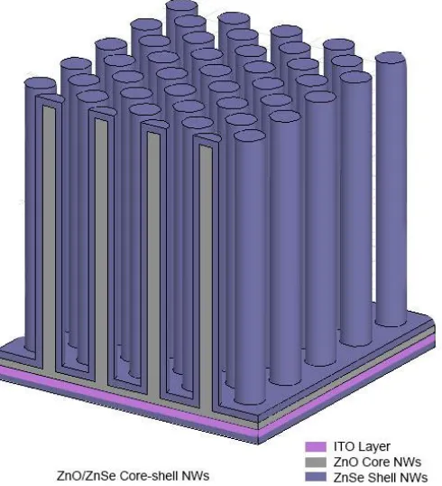
Figure 1.1 Schematic representation of type II heterojunction ZnO/ZnSe core/shell nanowire array ...2
Figure 2.1 Schematic representation of the CVD Chemical Vapour Deposition process shows how ZnO NWs can be grown on ITO Substrate...8
Figure 3.1 SEM images of ZnO nanowire array on ITO substrate (a, b and c) top-view SEM images at different magnifications of ZnO Nanowire array on ITO substrate (d) Cross-sectional SEM image of ZnO nanowire array with an average length of 5μm...10
Figure 3.2 TEM image and EDX pattern of the as-synthesized ZnO/ZnSe core/shell heterostructures: (a) TEM image of the ZnO/ZnSe core/shell heterostructure tip and mid part of the nanowire. (b) The corresponding EDS spectrum of the samples taken from the NW tip, mid and root, respectively. The signals for C and Cu peaks is originated from the amorphous carbon substrate and the TEM grid substrate...12
Figure 4.1 Schematic illustration of the fabrication process of ZnO/ZnSe core/shell NWs. A-F, present commonly used configurations of the device integration. ...13
Figure 4.2 This schematic shows the temperature profiles for both zones. The central heating zone is labeled as a blue line and the right heating zone as a grey line. The approximate time consumed for cooling each zone is depicted as dashed lines...15
Figure 4.3 I–V Current–voltage characteristic of ZnO/ZnSe core/shell nanowire array photodetectors under different UV illumination densities as shown in Figure (a). Photocurrent response under variable UV illumination (b) and (c) calculated relative responsivity under various illumination densities...16
Figure 4.4 I–V Current–voltage characteristic of ZnO/ZnSe core/shell nanowire array photodetectors under different compressive loads. As shown in (a) and (b), the photocurrent response under different compressive loads when the illumination density is 0.04 mW cm-2 and
vi
vii
List of Tables
Table 1.1 Typical physical parameters of zinc oxide (ZnO)...3
viii
Abstract
A two-step synthesis was performed to fabricate type-II heterojunction ZnO/ZnSe core/shell nanowires. First, ZnO core NWs were synthesized on ITO substrate via chemical vapor deposition (CVD). Then pulsed laser deposition (PLD) technique was carried out to coat the ZnO core with ZnSe Shell. The ZnO/ZnSe core-shell NWs which has application on optoelectronics, such as photodetectors and photosensors were characterized via scanning electron microscope (SEM), transmission electron microscope (TEM) and finally photodetector devices were measured via current–voltage characteristics under ultraviolet (UV) illumination to investigate the effect of the inner piezopotential. The ZnO-nanowire-based photodetector ultraviolet (UV) light devices with core/shell structure show excellent photo-responsivities. Ultimately, the results in this work of ZnO/ZnSe core/shell heterojunction with excellent piezoelectric properties is demonstrated to show great promise in the piezo-phototronic device application.
1
Introduction and Background
Recent development advances have allowed wide band-gap II-VI compound semiconductors to
approach applications of these materials to fabricate novel devices, such as optoelectronic devices,
light emitting diode, laser diode, solar cell, sensor, pyroeletric & piezoelectric devices,
self-compensating gas sensor, substrate transparent electrode, electronic devices, filed-effect transistor,
high power electronic devices, low threshold optical pumping, SAW devices, SAW filter and SAW
oscillator. Wide band-gap II-VI compound semiconductors can be obtained when group II elements and group VI elements are combined in a synthetic way. In addition, wide-bandgap II– VI compounds such as ZnS, ZnO, ZnSe, ZnTe, CdSe and CdTe have been studied and applied to
optoelectronic devices like photodetectors or photosensors (1).
2
Figure 1.1 Schematic representation of type II heterojunction ZnO/ZnSe core/shell nanowire array
1.1 The basics of ZnO
Zinc oxide (ZnO) is a II-VI compound semiconductor, which is called a multifunctional material
due to its unique physical and chemical properties. Zinc oxide is an intrinsic n-type semiconductor
because of a deviation from stoichiometry, due to the presence of intrinsic defects such as oxygen
vacancies and zinc interstitials (4). Its application for optoelectronics refers to its physical and
chemical properties, such as high chemical stability, high electrochemical coupling coefficient,
broad range of radiation absorption and high photostability (5).
Zinc oxide is an attractive semiconductor material that displays semiconducting and piezoelectric
properties. It has been studied and found to be a very promising material for optoelectronic devices.
3
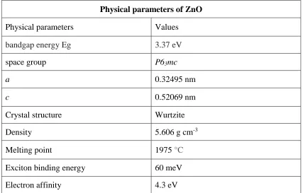
Additionally, zinc oxide mainly exhibits a wide and direct bandgap ~3.37 eV. Since the zinc oxide (ZnO) bandgap is too large for visible light absorption, it makes it very attractive for optoelectronic devices in the near UV region. Besides, the inherent piezoelectric property of ZnO can produce voltage output from applied stress. Therefore, the semiconducting and piezoelectric properties of ZnO means that it can be used as photodetectors(8).
Zinc oxide (ZnO) which is an important and promising metal oxide has been widely studied in
many areas because of its diverse properties and potential applications. ZnO as a semiconductor
has been used for medicinal purposes and in electronics, such as in laser diodes, LED’s, transparent
thin film coatings, and various piezoelectrics. Practically, it shows very promising application in
nanoscale range, such as ultralight UV detectors, actuators, transistors, sensors, etc (9).
Physical parameters of ZnO
Physical parameters Values
bandgap energy Eg 3.37 eV
space group P63mc
a 0.32495 nm
c 0.52069 nm
Crystal structure Wurtzite
Density 5.606 g cm-3
Melting point 1975 °C
Exciton binding energy 60 meV Electron affinity 4.3 eV
4
1.1 The basics of ZnSe
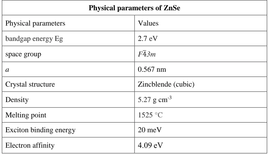
Zinc selenide (ZnSe), a II-VI compound semiconductor with cubic zinc blende structure and a direct bandgap of 2.7 eV, is considered a very favorable semiconductor material for optoelectronic devices. Due to its great bandgap as well, it has low optical absorption in the visible and infrared spectral region. It has potential to be used in optoelectronic devices such as light emitting diodes, optical coatings, ultrasonic transducers, and photodetectors due to its wide range of useful properties, such as large band gap, low resistivity and photosensitivity (12).
Physical parameters of ZnSe
Physical parameters Values
bandgap energy Eg 2.7 eV
space group F4̅3m
a 0.567 nm
Crystal structure Zincblende (cubic)
Density 5.27 g cm-3
Melting point 1525°C
Exciton binding energy 20 meV Electron affinity 4.09 eV
Table 1.2 Typical physical parameters of zinc selenide (ZnSe) (10) & (13).
1.2 Importance of piezo electronic materials
5
properties (15). These piezoelectric materials have been employed in an impressive range of applications, such as piezoelectric resonators, transducers, sound emitters, receivers, solar cells, photodetectors and LEDs. Moreover, sonar is a sound navigation and ranging, which is a device used for board ships, boats and submarines to detect other sonar objects under water. TMD is a tuned mass damper device that is used in skyscrapers at the top of the building as a motion control device. TMD is a system being used in skyscrapers to stabilize the building in the case that its stability is ever threaten by earthquakes, storms, or heavy winds (16). Therefore, piezoelectric materials are very important in our lifestyle and in the following paragraphs the coupling system, important definitions, effects and mechanism of these materials will be discussed.
Piezoelectric potential or piezopotential is created when pressure/stress is applied upon the
piezoelectric material. For instance, there are several ways that the coupling system can be
combined and therefore each coupling system or sometimes combination of them can be used for
a variety of applications of the piezoelectric material,such as Piezotronics, Piezophotonics,
Opto-electronics and Piezo phototronics. Piezotronics can be obtained when piezo-electricity and semiconductor are coupled, while by joining piezo-electricity and photonic excitation, a
Piezophotonics can be attained. Also, by coupling the semiconductor and photonic excitation, a
Piezo phototronics can be achieved. Finally Piezo-phototronics is a result of the three-way-coupling between piezo-electricity, photonic excitation and semiconductor. Consequently, by using piezoelectric semiconductor materials, the piezoelectric, photoexcitation and semiconducting properties can be coupled together to investigate their physics and novel applications (17).
The elements ZnO, GaN, InN, and CdS in group II-VI and III-V in the periodic table are wide bandgap semiconductor materials that possesses piezopotential, which in turn leads them to be fabricated as a device causing their piezoelectric potential to be used. The piezopotential is an
inner potential inside the crystal that is formed by non-mobile, non-annihilative ionic charges.
6
significantly boost piezopotential inside the nanowire and this in turn improves charge carrier transport (18) and (19).
Recently, rapid progress in the dominant fields of piezo-phototronics and piezotronics has been observed. The significance of the piezo-phototronic devices are to use the inherent piezoelectric polarization to tune the charge generation, separation, and transport and/or recombination process at the interface for enhancing optoelectronic processes, while piezotronics is about using the built-in piezopotential as a ‘gate’ voltage to adjust charge-carrier transport across the metal– semiconductor contact or the p–n junction. Piezoelectric charges at the interface/junction can significantly affect the charge carrier separation and transport. For instance, when optoelectronic
devices are fabricated using piezo-phototronic effect, their performance and interaction with light
are significantly changed by externally applied strain. Finally, charge generation, separation, transport and recombination process are the essential physics of piezotronic and piezo-phototronics devices (20).
As it is very well known, piezoelectric materials can be used to convert mechanical energy into electric energy and vice versa. For instance, when an external voltage is applied to devices fabricated using the piezoelectric potential like sensors and actuators, a mechanical action or geometric deformation occurs, and this phenomena is known as “Inverse Piezoelectric Effect”. Also, when piezoelectric semiconductor materials are under externally applied forces, an electric filed “voltage” will be generated, and this phenomena is called “Direct Piezoelectric Effect” (17) and (20).
7
Growth of ZnO nanowire
2.1 Background
The growth techniques of ZnO are very important since they influence their structure and since there are a lot of techniques to synthesize ZnO NWs, the choice method to make ZnO NWs for optoelectronic device is a crucial step. Choosing the appropriate method allows one to take advantage of its useful properties. Zinc oxide naturally crystallizes in wurtzite structure. ZnO which has a melting point of 2248 K typically show three types of growth direction like [211̅̅̅̅0], [011̅0] or [0001] (21).ZnO single crystals and semiconductors II–VI compounds can be epitaxially grown in a variety of ways, such as the hydrothermal method, vapour liquid solid (VLS) (22), liquid-phase epitaxy (LPE) (23), hot-wall epitaxy (HWE) (24), metalorganic chemical vapor deposition (MOCVD) (25) or metalorganic phase epitaxy (MOVPE) (26), molecular-beam epitaxy (MBE) (27) and atomic-layer epitaxy (ALE) (28). Therefore, the method being used for growing ZnO NWs can contribute to its properties and by taking advantage of the morphologies will therefore effectively enable scientists to optimize optoelectronic devices.
2.2 ZnO nanowire array grown on ITO by CVD
8
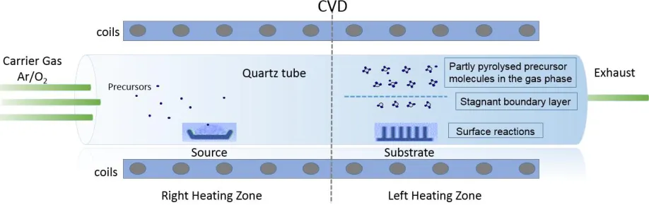
Figure 2.1 Schematic representation of the CVD Chemical Vapour Deposition process shows how ZnO NWs can be grown on ITO Substrate.
Synthesis
The ZnO powder was loaded into an alumina boat as the source material. Cleaned ITO substrates (area, 1 cm x 1 cm) were placed downstream of the precursor. The furnace was heated to a preset temperature and maintained at this temperature for 60 minutes. A mixture of Ar/O2 as carrier gases,
9
Core-shell ZnO and ZnO/ZnSe synthesis
3.1 ZnO/ZnSe core-shell nanowire array by PLD method
In the past decade, pulsed laser deposition, PLD, is considered a very exciting technique that has been widely used and applied for a variety of materials. It has been extensively utilized to deposit or coat thin films for superconductors, semiconductors and insulators. The idea of this technique is based on the interaction of a pulsed laser beam with the surface of a solid target (31). The PLD of a semiconductor compound has been successfully carried out in our research group for optoelectronics and solar cell application with good optical properties (32) (33) and (34).
Thin films properties, such as crystalline structure, thickness, stoichiometry and composition, can be controlled by using pulsed laser deposition, PLD, technique. Moreover, excellent coating properties can be obtained through low deposition temperatures. However, PLD has a series of disadvantages, some examples of this are that roughness and clusters may appear at the surface resulting in bad optical and electrical properties. Additionally, it cannot be made into larger amounts (35).
10
3.2 Structures analysis of ZnO/ZnSe core-shell nanowire
A two-step synthesis has been utilized to fabricate type II heterojunction ZnO/ZnSe core/shell nanowire array. First, as-grown ZnO NWs on ITO substrates (area, 1 cm x 1 cm), their samples were taken to be examined by Scanning Electron Microscope, SEM, to look for morphological and structural details of the as-synthesized ZnO. Subsequently, the ITO substrate with ZnO nanowire array was taken to perform a coating layer of ZnSe layer on the surface of NWs.
Figure 3.1 SEM images of ZnO nanowire array on ITO substrate (a, b and c) top-view SEM images at different magnifications of ZnO Nanowire array on ITO substrate (d) Cross-sectional SEM image of ZnO nanowire array with an average length of 5μm
11
12
Figure 3.2 TEM image and EDX pattern of the as-synthesized ZnO/ZnSe core/shell heterostructures: (a) TEM image of the ZnO/ZnSe core/shell heterostructure tip upper and mid lower pictures. (b) The corresponding EDS spectrum of the samples taken from the NW tip, mid- and root, respectively. The signals for C and Cu peaks is originated from the amorphous carbon substrate and the TEM grid substrate, respectively.
13
spectrometer (EDS) was conducted to investigate the coated ZnO/ZnSe core/shell nanowire array structure. Figure 3.2(a) displays a typical low-magnification TEM image of a ZnO/ZnSe core/shell nanowire array heterostructures. The interface region between the ZnO core and ZnSe shell is clearly observed and the thickness of the ZnSe shell is about 18 nm. For further investigation, the corresponding EDS spectrum was conducted on tip middle and root of a single core/shell nanowire structure. Figure 3.2(b) shows the composition distribution of the as-synthesized ZnO/ZnSe core-shell nanowire array heterostructures, the spatial distribution of the ZnO and ZnSe elements in the core and shell, respectively, were obtained by using EDS spectrum. The spectrum exhibits strong Zn and Se peaks indicating the formation of ZnSe product. The C and Cu signals come from the amorphous carbon substrate and the TEM grid, respectively.
Device processing and measurements
4.1 Experimental
14
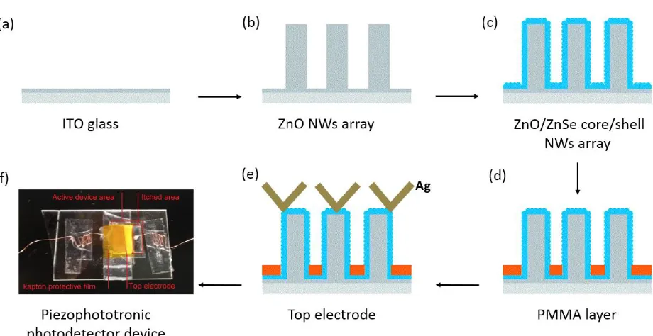
Figure 4.1 illustrates the brief fabrication of the final ZnO/ZnSe core/shell nanowire array heterostructures photodetector devices. After providing several procedures including: 4.1(a), ITO substrate with standard wafer cleaning procedure; 4.1(b), ZnO NWs grown on ITO sub. via CVD method; 4.1(c), ZnSe product as a shell coated on ZnO core using PLD technique; 4.1(d), PMMA layer spin-coated on ZnO/ZnSe core/shell; 4.1(e), Ag/polyester zigzag electrode on the tips of ZnO/ZnSe core/shell; 4.1(f), finished device structure where the device was integrated as followed. First, the portion of the ITO mother substrate was etched using diluted HCl so that a copper wire can be attached directly to the ITO surface. Second, after connecting a copper wire to the Ag/polyester zigzag using a silver paste, the top electrode was placed on the top of the ZnO/ZnSe and then kapton protective film was used to package the device.
Growth of ZnO nanowires NWs by Chemical Vapour Deposition (CVD)
The synthesis of ZnO nanowires was conducted on SiO2 passivated indium tin oxide (ITO) coated
glass substrate (Rs = 70 – 100 Ω) (area, 1 cm x 1 cm) via Chemical Vapour Deposition. ZnO NWs
were initially synthesized on a cleaned ITO substrate to cover the entire substrate surface. The CVD system contained a horizontal quartz tube furnace with three heating zones, however only the central and right zones were used. Firstly, 4.0 g of high purity metallic Zn powder (Alfa Aesar, 99.9% purity, metals basis) as the source material was loaded into a ceramic boat and placed inside the chamber at the central heating zone. The target substrates were placed downstream of the Zn powder ceramic boat at the right zone. The target to the substrate distance was about 15 centimeters. Prior to heating, the system was pumped down to 1 x 10⁻³ Torr and filled with inert gases Ar/O2. Argon and Oxygen gases with 40 and 300 SCCM flow rate, respectively, were
15
Figure 4.2. This graph shows the temperature profiles for both zones. The central heating zone is labeled as a blue line and the right heating zone as a grey line. The approximate time consumed for cooling each zone is depicted as dashed lines.
Deposition of ZnSe layer by pulsed laser deposition (PLD)
In order to synthesize ZnO/ZnSe core/shell nanowires, a single ITO substrate with as-grown ZnO nanowires was transferred into a pulsed laser deposition system. LOTIS TII LS-2147 Pulsed Nd:YAG Laser was applied to ablate the target. The laser wavelength, energy density, and pulse frequency were 1064 nm, 45 mJ cm-2, and 3 Hz, respectively. The target substrate was loaded in a
quartz tube and placed near the ZnSe target disc where the target source was cold-pressed into a pellet and placed into a ceramic boat. The quartz tube placed inside the furnace was first vacuumed 1 x 10⁻³ Torr base pressure one hour before raising the temperature. Then the temperature of the furnace was ramped gradually to 500 °C and left at this temperature during the deposition process, which lasted for 10 minutes. After the deposition process took place, the chamber was allowed to cool down naturally. Finally, the coating of ZnSe layer on the ZnO NWs surface was successfully carried out and the substrate was ready for structural, optical characterizations and device fabrication.
0 200 400 600 800 1000
0 50 100 150 200 250 300 350 400 450
Tem
p
(
°c)
Time (min)
16
4.2 Piezo-phototronic photodetector performance of ZnO/ZnSe nanowire
array
Piezo-phototronic photodetector
-1.5 -1.0 -0.5 0.0 0.5 1.0 1.5
-0.4 -0.2 0.0 0.2 0.4 0.6 0.8 1.0 Curr en t ( mA) Voltage (V) Dark
0.04 mW cm-2
0.12 mW cm-2
0.44 mW cm-2
0.92 mW cm-2
1.12 mW cm-2
1.32 mW cm-2 (a)
0.0 0.3 0.6 0.9 1.2 1.5
0.1 0.2 0.3 0.4 0.5 0.6 0.7 (b) Iill -Ida rk (µA)
Intensity (mW cm-2
)
0.0 0.2 0.4 0.6 0.8 1.0 1.2 1.4
0.0 0.5 1.0 1.5 2.0 2.5 3.0 3.5 (c) Respo nsivity ( mA/w)
Intensity (mW cm-2
)
Figure 4.3 IV Current–voltage characteristic of ZnO/ZnSe core/shell nanowire array photodetectors under different UV illumination densities as shown in Figure (a). Photocurrent response under variable UV illumination (b) and (c) calculated relative responsivity under various illumination densities
17
the photocurrent increases when UV illumination density is increased, which means an increment of electron–hole pair rate occurs due to the effect of higher intensity. Figure 4.3(b) exhibits photocurrent versus illumination intensity plotting that was taken from Figure 4.3(a) where a pronounced increase in photocurrent curves appear in proportion to the light intensity. The responsivity (Rλ) at a particular wavelength was calculated and plotted as shown in Figure 4.3(c).
The responsivity equation at a practical wavelength is described as follows (39)
𝑅
λ=
𝐼𝑙𝑖𝑔ℎ𝑡− 𝐼𝑑𝑎𝑟𝑘
𝑃𝑖𝑙𝑙
Where,
I light = Current when the photodetector is under illumination
I dark= Current when the photodetector is in the dark
P ill = Excitation power
And light intensity (Pill) can be calculated as
𝑃
𝑖𝑙𝑙= 𝐼
𝑖𝑙𝑙× 𝐴
Where,
I ill = Illumination density
A = Active illuminated device area
18
-1.5 -1.0 -0.5 0.0 0.5 1.0 1.5
-0.3 0.0 0.3 0.6 0.9 (a) Curr en t ( mA) Voltage (V) Strain=0.00 kgf Strain=0.05 kgf Strain=0.10 kgf Strain=0.20 kgf
-1.5 -1.0 -0.5 0.0 0.5 1.0 1.5
-0.3 0.0 0.3 0.6 0.9 1.2 Curr en t ( mA) Voltage (V) Strain=0.00 kgf Strain=0.05 kgf Strain=0.10 kgf Strain=0.20 kgf (b)
0.0 0.1 0.2
0.4 0.5 0.6 0.7 0.8 0.9 (c) ILoad -I0 (m A) Load (kgf)
0.0 0.1 0.2
0.5 0.6 0.7 0.8 0.9 1.0 1.1 (d) ILoad -I0 (m A) Load (kgf)
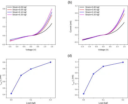
Figure 4.4 IV Current–voltage characteristic of ZnO/ZnSe core/shell nanowire array photodetectors under different compressive loads. As shown in (a) and (b), the photocurrent response under different compressive loads when the illumination density is 0.04 mW cm-2 and 0.12 mW cm-2, respectively. Figure (c) and (d) display photocurrent response with respect to
compressive loads for (a) and (b), respectively.
To investigate the influence of the inherent piezopotential of ZnO/ZnSe core/shell nanowire array
19
which is reasonable. Additionally, the photocurrent peaks can be recovered as the compressive load was released. Figures 4.4(c) and 4.4(d) are the plotted result for the change in peak photocurrent versus compressive load for figures 4.4(a) and 4.4(b). The current mA for 0.04 mW cm-2 and 0.12 mW cm-2 illumination is significantly enhanced from 0.4 mA to 0.9 mA and from 0.5 mA to 1.1 mA, respectively, by introducing the compressive load, although the compressive load has little effect on the sensitivity to stronger light illumination. Therefore, the detection sensitivity of the nanowire-based photodetector is enhanced upon the UV light illumination when the ZnO NWs experiences compressive load.
Energy Band Diagram
Figure 4.5 Schematic diagram displays type-II energy band alignment of ZnO/ZnSe heterojunction. The solid lines (green and red) in (a) show the natural band alignments, and the black dashed line shows Fermi level for both ZnO/ZnSe. (b) Thedashed lines show the original conduction and valence band, respectively, and curved lines indicate the effective band gap position when the silver coated polyester zigzag electrode is being positioned on the top of nanowires array. (c) Under UV illumination only and (d)under applied load (32) & (37).
20
ZnO/ZnSe core/shell nanowire array photodetector, a schematic band diagram has been drawn to show energy band realignment in different states. As shown in the diagram above, (a) natural band alignments, (b) sliver Ag zigzag on the top of core/shell structure, (c) under UV illumination only and (d) under compressive load and UV light. Figure 4.4(a) displays the type-II heterostructures band alignment of ZnO/ZnSe. When silver zigzag has not been attached, the Fermi level of ZnSe is higher than ZnO where the bandgap, electron affinities and work function for ZnO and ZnSe are equal to 3.37 eV, 2.7 eV, 4.3 eV, 4.09 eV, 5.3eV and 4.84eV, respectively. All values were taken from publications (10, 11 and 13). The vacuum level is defined as the energy of the electron at rest far from the influence of the potential of the solid and the work function is the energy required to take an electron from the Fermi level to the vacuum level, while the electron affinity of a semiconductor is the energy required to remove an electron from the bottom of the conduction band to the vacuum level (32) and (37).
In Figure 4.4(b), as the fermi level of ZnSe is higher, it means that there are more energy states in ZnSe than ZnO. Now, when Ag silver zigzags into contact, electronic flow will occur to balance the charge imbalance in the composite material. In other words, the shifting of energy bands continues until the energy levels EFM,ZnO and EFM,ZnSe are equalized. Therefore, after both EFM,ZnO
and EFM,ZnSe have reached equilibrium energy or gotten to the same level, a downward bending of
EC,ZnSe and EV,ZnSe took place. For a semiconductor, when an intense ultraviolet UV light excites
band to band transitions, additional energy gaps can evolve within the original bands. Therefore, a weak type II transition occurred between EC,ZnSe and EV,ZnSe as shown in Figure 4.4(c) Upon
21
Conclusion
In summary, an enhanced photoresponse of type II ZnO/ZnSe heterostructures nanowire array with the ZnSe coated-NW-array as the shell and ZnO NW array as the core was developed. The photodetector displayed sensitive photoresponse to different light intensity 0.04, 0.12, 0.44, 0.92, 1.12 and 1.32 mW cm-2 with an external bias of 1.5 V. The excellent photoresponse of the photodetector device is due to the abrupt interface between ZnO and ZnSe. In addition, when compressive load was subjected to the photodetectors, the performance of the ZnO/ZnSe devices were further enhanced by order of magnitudes under UV illumination. This investigation demonstrates that the ZnO/ZnSe core/shell nanowires has a potential for photodetection with enhanced photoresponsivity.
22
REFERENCES
1- Kasap, S. O., & Capper, P. (2006). Springer handbook of electronic and photonic materials. New York: Springer
2- Cho, S., Jang, J., Lim, S., Kang, H., Rhee, S., Lee, J., & Lee, K. (2011). Solution-based fabrication of ZnO/ZnSe heterostructure nanowire arrays for solar energy conversion. Journal of Materials Chemistry, 21(44), 17816-17822.
3- Boxberg, F., Søndergaard, N. and Xu, H. Q., Photovoltaics with piezoelectric core-shell nanowires. AIP Conference Proceedings, (2011) 1399(1), 469-470.
4- Anderson, J, Chris G, V and de, W, Fundamentals of zinc oxide as a semiconductor. Reports on Progress in Physics. (2009) 72, 12, 126501.
5- Kołodziejczak-Radzimska, A. and Jesionowski, T. Zinc Oxide—From Synthesis to Application: A Review. Materials (2014), 7, 2833-2881.
6- Bacaksiz, E., Parlak, M. and Tomakin, M. The effect of zinc nitrate, zinc acetate and zinc chloride precursors on investigation of structural and optical properties of ZnO thin films. J. Alloy. Compd. (2008), 466, 447‒450.
7- N. Izyumskaya , V. Avrutin and Ü. Özgür, Preparation and properties of ZnO and devices, Phys. Status Solidi B (2007) 1439–1450
8- Alivov Ya. I., Liu C., Teke A. and Reshchikov M. A., A comprehensive review of ZnO materials and devices. J. Appl. Phys. (98), pp. 041301(103)
9- Tian, Wei, Hao Lu, and Liang Li, "Nanoscale ultraviolet photodetectors based on onedimensional metal oxide nanostructures. Nano Research. 8, 2, 382, (2015).
10-Takahashi, K., Sandhu, A., and Yoshikawa, A., Wide Bandgap Semiconductors: Fundamental Properties and Modern Photonic and Electronic Devices. Berlin, Heidelberg: Springer-Verlag Berlin Heidelberg, 2007.
11-Wang, ZL and Song, J., Piezoelectric Nanogenerators Based on Zinc Oxide Nanowire Arrays. Science. 5771, 242, 2006. ISSN: 00368075.
12-Ashraf M., Akhtar S. and Khan A., Effect of annealing on structural and optoelectronic properties of nanostructured ZnSe thin films. Journal of Alloys and Compounds, (2015) 2011; 509:2414-2419.
23
14-Manbachi, A., and Cobbold, R. C., Development and application of piezoelectric materials for ultrasound generation and detection. Ultrasound, (2011) 11(4), 187-196. 15-Zhao W., Xumin P. and Yahua H.,Piezoelectric Nanowires in Energy Harvesting
Applications, (2015) vol. 2015 pp 165631, 21
16-D.J. Jones, S.E. Prasad, J.B. Wallace, "Piezoelectric Materials and their Applications", Key Engineering Materials, (1996) Vols. 122-124, pp. 71-144
17-WANG, ZL. Review: Piezopotential gated nanowire devices: Piezotronics and piezo-phototronics. Nano Today. (2010) 5, 540-552.
18-Boxberg, F, Sondergaard, N and Xu, HQ. Elastic and piezoelectric properties of zincblende and wurtzite crystalline nanowire heterostructures. Advanced Materials (2012) 24: 4692–706.
19-M. Vos, F. Xu and J. H. Weaver, “Influence of metal interlayers on Schottky barrier formation for Au/ZnSe (100) and Al/ZnSe (100),” Applied Physics Letters, vol. 53, no. 16, pp. 1530–1532, 1988.
20-Liu Y., Zhang Y. and Yang Q., Fundamental theories of piezotronics and piezo-phototronics. Nano Energy. (2015) 2014.11.051.
21-Xiang Y. K. and Zhong L. W., Polar-surface dominated ZnO nanobelts and the
electrostatic energy induced nanohelixes, nanosprings, and nanospirals. Applied Physics Letters. (2004) 84(6):975-977.
22-Zhong Lin Wang,Zinc oxide nanostructures: growth, properties and applications, J. Phys. Matter 16 (2004) R829–R858
23-J. Kobayashi, H. Sekiwa and M. Miyamoto, Crystal Growth & Design (2009) 9 (2), 1219-1224
24-A. Lopez-Otero: Thin Solid Films 49, 1 (1978)
25-Tak, Y. J.; Ryu, Y. H.; Yong, K. Nanotechnology (2005), 16, 1712 26-H. M. Manasevit, W. I. Simpson: J. Electrochem. Soc.118, 644 (1971)
27-Bjork, M. T. Ohlsson, B. J. Sass, T and Persson, A, Appl. Phys. Lett. (2002), 80, 1058. 28-T. Suntola: Mater. Sci. Rep. 4, 261 (1989)
24
30-Anthony c. J. and michael l. H., Overview of Chemical Vapour Deposition, (2008) ISBN: 978-0-85404-465-8.
31-E. Morintale, C. Constantinescu and M. Dinescu, Thin films development by pulsed laser-assisted deposition, physics auc, (2010) vol. 20, 43-56
32-S. C. Rai, K. Wang and Y. Ding, Piezo-phototronic Effect Enhanced UV/Visible Photodetector. ACS Nano (2015) 9 (6), 6419-6427
33-Wang, K., Chen, J.and Zhou, W., Direct Growth of Highly Mismatched Type II
ZnO/ZnSe Core/Shell Nanowire Arrays on Transparent Conducting Oxide Substrates for Solar Cell Applications. Advanced Materials, (2008) 20(17), 3248.
34-S. Wozny, K. Wang, and W. Zhou, Cu2ZnSnS4 nanoplate arrays synthesized by pulsed laser deposition with high catalytic activity as counter electrodes for dye-sensitized solar cell applications, Journal of Materials Chemistry A: Materials for Energy and
Sustainability (2013), 1(48), 15517-15523.
35-Venkatachalam S., Mangalaraj D. and Narayandass S., Influence of substrate temperature on the structural, optical and electrical properties of zinc selenide (ZnSe) thin films. (2005) 39, 22, 4777-4782
36-Perna G., Capozzi V., and Plantamura M., Structural and optical properties of pulsed laser-deposited ZnSe films. Applied Surface Science, (2002) Volume 186, Issues 1–4 521-526.
37-Chen W., Zhang N. and Zhang M. Y., Controllable growth of ZnO-ZnSe heterostructures for visible-light photocatalysis, Cryst. Eng. Comm., (2014) vol. 16, no. 6, pp. 1201–1206. 38-J. H. Simmons and K. S. Potter, Optical Materials, Academic Press, N Y. (2001) 35,
131-133. ISSN: 0143-8166.
25
VITA