ScholarWorks@UNO
ScholarWorks@UNO
University of New Orleans Theses and
Dissertations Dissertations and Theses
12-17-2004
A System-on-Programmable-Chip Approach for MIMO Lattice
A System-on-Programmable-Chip Approach for MIMO Lattice
Decoder
Decoder
Vipul Hiralal Patel University of New Orleans
Follow this and additional works at: https://scholarworks.uno.edu/td
Recommended Citation Recommended Citation
Patel, Vipul Hiralal, "A System-on-Programmable-Chip Approach for MIMO Lattice Decoder" (2004). University of New Orleans Theses and Dissertations. 192.
https://scholarworks.uno.edu/td/192
This Thesis is protected by copyright and/or related rights. It has been brought to you by ScholarWorks@UNO with permission from the rights-holder(s). You are free to use this Thesis in any way that is permitted by the copyright and related rights legislation that applies to your use. For other uses you need to obtain permission from the rights-holder(s) directly, unless additional rights are indicated by a Creative Commons license in the record and/or on the work itself.
MIMO LATTICE DECODER
A Thesis
Submitted to the Graduate Faculty of the University of New Orleans
in partial fulfillment of the requirements for the degree of
Master of Science in
The Department of Electrical Engineering
by
Vipul Hiralal Patel
B.S., University of Pune, 2000
ii
Acknowledgements
I would like to express my gratitude to my Advisor, Dr Xinming Huang, for his
support and timely advice through out my research. I appreciate and value his consistent
feedback on my progress, which was always constructive and encouraging, and
ultimately drove me to the right direction.
I would like to express my sincere thanks to the other committee members, Dr.
Jing Ma and Dr. Dimitrios Chalarampidis for their willingness to be on my thesis
committee. Their invaluable suggestions and insightful comments have made my work
more presentable.
I take this opportunity to thank my parents and wife for their unconditional love
and support through out my life. Finally I express my gratitude to my friends for their
iii
LIST OF ILLUSTRATIONS ...v
List of Figures ...v
List of Tables ...vi
Glossary of Abbreviations ...vii
ABSTRACT...viii
1. Introduction...1
1.1 Motivation for Implementing MIMO Lattice Decoder...1
1.2 Research Objectives ...2
1.3 Thesis Contribution...2
1.4 Organization of Thesis ...3
2. Introduction to Altera System-on-Chip ...4
2.1 Introduction of Nios Development Board...4
2.2 General Description ...5
2.2.1 EP1S10 Device ...6
2.2.2 Flash Memory Device ...7
2.2.3 Serial Port Connector...7
2.3 Design Tools ...8
2.3.1 Quartus II ...8
2.3.2 SOPC Builder...8
2.3.3 DSP Builder ...9
2.4 System Components...10
2.4.1 CPU Architecture ...11
2.4.2 Instruction Set ...12
2.4.3 Register File ...12
2.4.4 Cache Memory...12
2.4.5 Exception Handling ...13
2.4.6 Hardware Acceleration ...13
2.4.7 Custom Instructions ...14
2.4.8 Standard CPU Options ...15
3. Multiple Input Multiple Output Systems and Lattice Decoder...16
3.1 Multiple Input Multiple Output System...16
iv
3.1.2 Receiver ...17
3.2 Closest Point Search in Lattices...18
3.2.1 Conceptual Description of Closest Point Search Algorithm...19
4. Algorithms ...21
4.1 Decoder ...21
4.2 A Geometric view of square root ...25
4.3 Strassen Matrix Inversion Method ...31
4.3.1 Reduction of Strassen Matrix Inversion algorithm of 4x4 lower triangular matrix...34
4.4 QR Decomposition of Matrix ...36
4.4.1 Householder Matrix ...37
5. Prototyping of Closest Point Search Algorithm ...41
5.1 Why System-on-Chip? ...41
5.2 Prototyping Closest Point Search Algorithm ...41
5.2.1 Interface between Nios microprocessor based system and controller ...43
5.2.2 Interface between state A, B, C and Controller ...44
5.2.3 VHDL Code structure of Controller for Interface with state A, B, C...45
6. Results ...47
References ...54
v
List of Illustrations
List of figures:
Figure 2.1 Nios Development Board...4
Figure 2.2 Nios Processor Based System...11
Figure 2.3 Custom Instruction Logic ...14
Figure 3.1 MIMO Transmitter...16
Figure 3.2 MIMO Receiver ...16
Figure 4.1 Flowchart of Decoding Algorithm...22
Figure 4.2 Flowchart of State A of Decoding Algorithm...23
Figure 4.3 Flowchart of State B of Decoding Algorithm...23
Figure 4.4 Flowchart of State C of Decoding Algorithm...24
Figure 4.5 Geometric view of the square of three digit number ...26
Figure 4.6 Geometric view of the square of three digit number ...26
Figure 4.7 Flow chart of Square Root Algorithm ...30
Figure 4.8 Flow chart of Strassen Matrix Inversion Algorithm ...33
Figure 4.9 Flowchart of QR Decomposition Algorithm ...40
Figure 5.1 Hardware architecture of Lattice Decoder. ...42
Figure 5.2 Interface between controller and Nios Microprocessor based system...43
vi
List of Tables:
Table 2.1 Stratix EP1S10 Device Features ...6
Table 2.2 Comparison of Different Nios Processor Multipliers ...15
Table 6.1 Comparison of Nios Processor with and without divider to perform Division...48
Table 6.2 Comparison of “sqrt” function in C language and square root algorithm ...48
Table 6.3 Number of cycles required to invert 4x4 and 8x8 lower triangular matrix using Starssen method ...49
Table 6.4 Number of cycles to perform QR Decomposition of 4x4 matrix ...50
Table 6.5 Number of cycles required to perform pre processing part of decoding ...50
Table 6.6 Sequence of state in Matlab ...51
Table 6.7 Sequence of state in VHDL ...51
vii
Glossary of Abbreviations
MIMO – Multiple Input Multiple Output
FPGA – Field Programmable Gate Arrays
DSP – Digital Signal Processing
VHDL – Very High speed integrated Description Language
viii
Abstract
The past decade has shown distinct advances in the theory of multiple input multi output
techniques for wireless communication systems. Now, the time has come to demonstrate
this progress in terms of applications. This thesis introduces implementation of
Schnorr-Euchner strategy based decoding algorithm applied on Altera system-on-chip (Stratix
EP1S10F780C6) with Nios embedded processor. The lattice decoder is developed on
FPGA using VHDL. The preprocessing part of algorithm is targeted for Nios embedded
processor using C language. A controller is also designed to interface and communicate
Chapter 1
Introduction
1.1 Motivation for Implementing MIMO Lattice Decoder
Wireless systems are rapidly developing to provide high speed voice, text and multimedia
messaging services. To support these services, channels with large capacities are
required. The most brute- force approach to increasing wireless data rate is to use more
frequency channels to increase modulation rate. This "channel bonding" approach will
not meet the needs of WLAN consumers, for many reasons. First, while channel bonding
increases data rate, it decreases range for the same transmit power. Second, channel
bonding robs channels from other systems that operate nearby. Finally, channel bonding
violates government regulations in Japan and some European nations [12]
MIMO answers the question of how to achieve higher data rates with longer
range, backward compatibility, global regulatory compliance, all without using more
frequency spectrum. MIMO systems use multiple transmit and receive antennas. A
high-rate data stream is divided into multiple lower-high-rate streams, each of which is modulated
and transmitted through a different antenna at the same time using the same frequency
channel. Because of multipath reflections, each receive antenna output is a linear
the receiver using algorithms that rely on estimates of all channels between each
transmitter and each receiver. In addition to multiplying throughput, range is increased
because of an antenna diversity advantage, since each receive antenna has a measurement
of every transmitted data stream. The MIMO algorithm and its architecture are active
research area in wireless communication that motivated the research in MIMO systems.
1.2 Research Objectives
The main objectives of this thesis is to develop a system-on-chip approach for MIMO
lattice decoder by using closest point search algorithm described in [1] and also to utilize
parallelism offered by FPGAs to achieve high data rate.
1.3 Thesis Contribution
The implementation of lattice decoder has two parts: 1) the preprocessing part and 2) the
decoding part. To achieve high decoding rate, the decoding part can be implemented by
developing customized hardware unite (IP core) in a FPGA. The preprocessing part
contains operation like matrix inversion. Developing a special hardware unite to directly
implement it in FPGA is complicated and not efficient. Since speed requirement for
preprocessing part is not as critical, the microprocessor based system is suitable for the
preprocessing part. This thesis explains how to implement preprocessing part on an
embedded processor system together with the decoding part on a FPGA. The main
contribution of this thesis is that it explains how to develop embedded processor based
1.4 Organization of Thesis
Chapter 2 describes Altera system-on-chip. It addition, it describes how to develop the
whole system using SOPC builder and Quartus II software. It also describes hardware
acceleration techniques. Chapter 3 gives information about MIMO system. It also
describes details of closest point search algorithm. Chapter 4 describes Strassen matrix
inversion method, QR decomposition using Householder matrix, finding square root, and
decoding the closest point search algorithm as a part of decoder. Chapter 5 tells how to
develop interface between Nios processor based system and FPGAs. It also describes
parodying of closest point search algorithm. Finally, chapter 6 gives the simulation
Chapter 2
Introduction to Altera System-On-Chip
This chapter gives the introduction of Altera system-on-chip (Stratix
EP1S10F780C6). It also explains its programming techniques and how to develop the
whole system using SOPC builder and Quartus II software with hardware acceleration
techniques.
2.1 Introduction of Nios Development Board
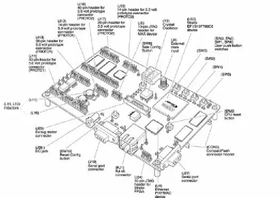
The figure 1.1 [7] shows Nios development board. It has following features:
1. Programmable chip Stratix EP1S10F780C6
2. 1 Mbytes of static RAM, 16 Mbytes of SDRAM, 8 Mbytes of flash memory
3. On board logic for configuring the programmable chip from flash memory
4. Two RS-232 serial ports for serial communication
5. 50 MHz clock generator
6. Dual 7-segment LED display and LCD display
7. JTAG connector which is used to load hardware image from host computer
2.2 General Description
The Nios development board, Stratix edition, provides a hardware platform for
developing embedded systems based on Altera Stratix devices. The Nios development
board features a Stratix EP1S10F780C6 device with 10,570 logic elements (LEs) and 920
Kbits of on-chip memory. When power is applied to the board, the on-board
configuration logic configures the Stratix FPGA using hardware configuration data stored
in flash. When the device is configured, the Nios processor design in the FPGA wakes up
and begins executing boot code from flash memory. User defined software and hardware
configuration data can be downloaded to the board from a host computer. Download
methods include a serial cable, a JTAG download cable, or an Ethernet cable. At power
on, or whe n the Reset, Config button (SW10 in figure1.1) is pressed, the configuration
controller reads user configuration data out of flash at address 0x600000. This data, and
suitable control signals, are used in an attempt to configure the FGPA. FPGA Image
“User Hardware Image”. If there is no valid User Hardware Image, or if SW9 (Safe
Config in figure1.1) is pressed, the configuration controller begins reading data out of
flash at address 0x700000. Any FPGA configuration data stored at this location is
conventionally called the “Safe Hardware Image”. The development board was factory
programmed with a “Safe Hardware Image”.
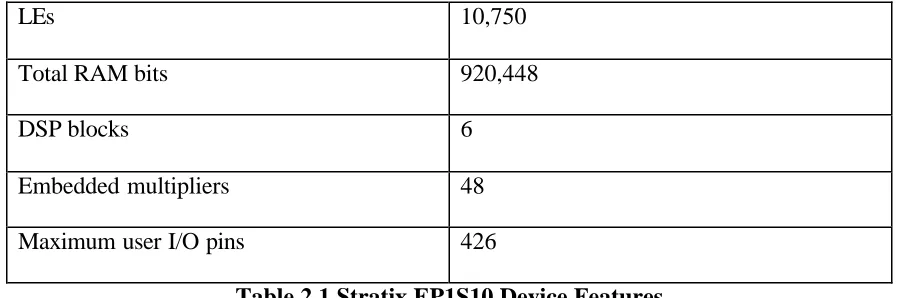
2.2.1 EP1S10 Device
Device U53 in figure1.1 is a Stratix EP1S10F780C6 FPGA in a 780-pin FineLine
BGA package. Table 1 lists the Stratix device features.
LEs 10,750
Total RAM bits 920,448
DSP blocks 6
Embedded multipliers 48
Maximum user I/O pins 426
Table 2.1 Stratix EP1S10 Device Features
There are two methods for configuring Stratix device:
1 By using the Quartus II software running on a host computer and JTAG connector,
we can download hardware image file into Stratix device.
2 Store hardware image into flash memory so that on board configure logic
2.2.2 Flash Memory Device
Device U5 in figure 1.1 is an 8 Mbyte AMD AM29LV065D flash memory chip
connected to the Stratix device and can be used for two purposes:
1. It can be used as general-purpose readable memory and non-volatile storage.
2. It is mainly used to store hardware image created by user or default hardware
image. It also used to store software program for Nios embedded processor.
2.2.3 Serial Port Connectors
J19 & J27 in figure1.1 are the serial connectors used for communication with a
host computer using a standard, 9-pin serial cable connected to the serial port of host
computer. The Nios board development provides two serial connectors, one labeled
Console and the other labeled Debug. Many processor systems make use of multiple
UART communication channels during prototype and debug stages. When we use
“printf” command in software code of Nios processor, the Nios system sends data to the
host computer using debug serial connector. Both connectors connect to the Stratix
FPGA in the same manner, and a Nios processor system can use either serial port for any
purpose, and is not limited to the usage implied by the label. Both FPGA logic ports are
able to transmit all RD-232 signals. Alternatively, the Stratix design may use only the
signals it needs, such as RXD and TXD. LEDs are connected to the RXD and TXD
2.3 Design Tools
Altera provides three design software tools to develop system on programmable
chip. They are:
1. Quartus II
2. SOPC builder
3. DSP builder
2.3.1 Quartus II
Quartus II is used to integrate Nios processor based system created using SOPC
builder with other hardware block. It is also used to synthesize system design and
download into Stratix EP1S10F780C6 device.
2.3.2 SOPC Builder
The SOPC builder is a system integration tool included in the Quartus II software
that provides designers with a powerful platform for composing memory- mapped
systems from common system components. SOPC Builder library components can be
either simple blocks of fixed logic, or complex, parameterized, and dynamically
generated subsystems. Examples of SOPC Builder library components include:
1. Processors (Excalibur stripe & Nios embedded processor)
2. Intellectual property (IP) & peripherals (including SOPC Builder Ready IP
cores)
3. Bridges (AMBA AHB-to-Avalon, Avalon-to-PCI)
In addition to the integrated FPGA solution generated, SOPC Builder provides software
files for developing simple to complex applications. Examples of the SOPC Builder file
outputs include:
1. Header files
2. Generic C drivers
3. OS kernels
4. Software Models for hardware-software co-simulation
2.3.3 DSP builder
DSP system design in Altera programmable logic devices requires both high- level
algorithm and hardware description language (HDL) development tools. The Altera DSP
Builder integrates these tools by combining the algorithm development, simulation, and
verification capabilities of The MathWorks MATLAB and Simulink system- level design
tools with VHDL synthesis, simulation, and Altera development tools. The DSP Builder
shortens DSP design cycles by helping designers create the hardware representation of a
DSP design in an algorithm- friendly development environment. The existing MATLAB
functions and Simulink blocks can be combined with Altera DSP Builder blocks and
Altera intellectual property (IP) MegaCore functions to link system- level design and
implementation with DSP algorithm development. DSP Builder allows system,
algorithm, and hardware designers to share a common development platform.
Designers can use the blocks in DSP Builder to create a hardware implementation of a
2.4 System Components
Nios embedded processor-based systems include one or more Nios CPUs and the
Avalon switch fabric. Nios processor-based systems can also contain multiple bus
masters, such as multiple Nios CPUs Designers can create and integrate these
multi-master systems easily when using Altera’s SOPC builder system development tool.
SOPC Builder automatically generates the interface to all of these components. The
following components can be used to form a Nios processor-based embedded system:
1. Nios CPU
2. Cache memory
3. Avalon switch fabric
4. Peripherals and memory interface
5. On chip debug
Designers can use SOPC Builder to custom-build Nios processor-based systems to their
own specifications. Figure 1.2 [7] shows an example of a Nios processor-based system
built using SOPC Builder. This particular system contains a Nios CPU with instruction
and data cache, an on-chip debugging core, a direct memory access (DMA) controller,
several peripherals such as UART, parallel I/O (PIO), an Ethernet port, and memory
Figure 2.2 Nios Processor-Based System
2.4.1 CPU Architecture
The Nios embedded processor CPU instruction set architecture is optimized for
programmable logic and system-on-a-programmable-chip (SOPC) integration. The Nios
CPU is a five-stage pipelined general-purpose RISC microprocessor that supports both
32-bit and 16-bit architectural variants. Both the 32-bit and 16-bit Nios CPUs utilize a
16-bit instruction format to reduce code footprint and instruction memory bandwidth. The
instruction set is optimized for compiled embedded applications. The Nios embedded
processor implements the CPU with separate data and instruction- memory bus masters,
generally known as modified-Harvard memory architecture. The SOPC builder allows
users to easily specify connections between both Avalos masters and slaves in a system.
These slaves may be memories or peripherals. Nios
CPU
D-cache
On-Chip Debug
DMA Controller I-cache
Avalon Switch Fabric
Data Memory
Instruction Memory
SDRAM Controller
UART
PIO
2.4.2 Instruction Set
The Nios instruction set is tailored to support compiled C and C++ programs. It
includes a standard set of arithmetic and logical operations and instruction support for bit
operations, byte extraction, data movement, control flow modification, as well as a small
set of conditionally executed instructions, which can be useful in eliminating short
conditional branches. The instruction set contains rich addressing modes to reduce code
size and increase the processor performance.
2.4.3 Register File
The Nios CPU architecture has a large general-purpose windowed register file,
several machine-control registers, a program counter, and the K register that is used for
instruction prefixing. The general-purpose registers are 32 bits wide in the 32-bit Nios
CPU and 16 bits wide in the 16-bit Nios CPU. The register file size is configurable and
contains a total of 128, 256, or 512 registers. The software can access the registers
exposed in a 32-register- long sliding window that moves with a 16-register granularity.
This sliding window allows fast context switching, accelerating subroutine calls and
returns.
2.4.4 Cache Memory
The configurable Nios CPU can optionally contain an instruction and data cache.
In general, cache is used to improve CPU performance by providing a local memory
implementation is a simple, direct- mapped, write-through architecture that is designed to
maximize performance and minimize device resource consumption.
2.4.5 Exception Handling
The Nios processor allows up to 64 vectored exceptions, which can be generated
from any of these three sources: external hardware interrupts, internal exceptions, or
explicit software trap instructions. The Nios exception-processing model allows precise
handling of all internally generated exceptions. Users can optionally disable support for
TRAP instructions, hardware interrupts, and internal exceptions. This option reduces the
size of the Nios system, and is intended for use only in systems where the processor is not
running complex software
2.4.6 Hardware Acceleration
The Nios instruction set can be configured to take advantage of hardware to
increase system performance. Specific cycle- intensive software operations can be
offloaded to hardware, increasing system performance significantly. This feature is
provided through instruction set modifications. The Nios processor has two levels of
instruction set modifications:
1. Custom instructions
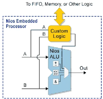
2.4.7 Custom Instructions
Developers can accelerate time-critical software algorithms by adding custom
instructions to the Nios processor instruction set. Developers can use custom instructions
to implement complex processing tasks in single-cycle (combinatorial) and multi-cycle
(sequential) operations. Additionally, user-added custom instruction logic can access
memory and/or logic outside of the Nios system. Figure 1.3 shows a block diagram of the
instruction logic[7].
Figure 2.3 Custom Instruction Logic
A complex sequence of operations can be reduced to a single instruction implemented in
hardware. This feature empowers developers to optimize their software inner loops for
digital signal processing (DSP), packet header processing, and computation- intensive
applications. The Altera SOPC builder software provides a graphical user interface (GUI)
that developers can use to add up to five of their own custom instructions to the Nios
2.4.8 Standard CPU Options
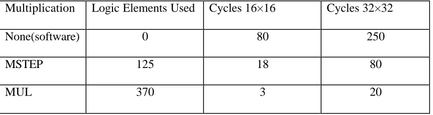
Altera provides several pre-defined instruction set extensions to increase software
performance. The MUL and MSTEP instructions are implemented with additional
hardware units. When you select either of these CPU options in the SOPC Builder, logic
is added to the arithmetic logic unit (ALU). For example, if a user chooses to implement
the MUL instruction, an integer multiply unit is added automatically to the CPU's ALU to
return a 16-bit by 16-bit multiplication operation in two clock cycles. This same
operation performed using an iterative software routine would take 80 clock cycles. Table
1.2 [7] shows number of clock cycles for multiplication using hardware and software
multiplier.
Multiplication Logic Elements Used Cycles 16×16 Cycles 32×32
None(software) 0 80 250
MSTEP 125 18 80
MUL 370 3 20
Table 2.2 Comparison of Different Nios processor Multipliers
Additionally, the Nios CPU includes an internal shift unit for executing logical and
arithmetic shift instructions. The CPU uses fixed barrel-shifter logic that executes all shift
operations in two clock cycles.
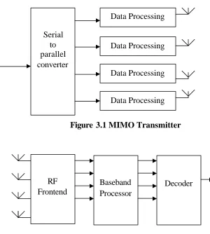
Serial to parallel converter
RF Frontend
Baseband Processor
Decoder
Chapter 3
Multiple Input Multiple Output Systems and Lattice Decoder
This chapter explains the concept of multiple input multi output (MIMO). It also
explains the closest point search algorithm used as the channel decoder in MIMO
receiver.
3.1 Multiple-input multiple output (MIMO) system
Figure 3.1 MIMO Transmitter
The diagrams shown above are schematic representation of multiple input multiple output
(MIMO) systems [4]. MIMO systems use multiple antennas in both transmitters and
receivers.
3.1.1 Transmitter
At transmitter side, the incoming serial stream of data is first converted into M
parallel streams. After de- multiplexing of serial data, M parallel data streams are
processed and transmitted using M antennas.
3.1.2 Receiver
The MIMO receiver has three main parts RF-frontend, baseband processor and
decoder.
(i) RF-frontend: It receives data from N parallel antennas and converts analog
data into digital form.
(ii) Baseband processor: It receives samp les from RF- frontend, extracts timing
information and channel information (channel matrix coefficients).
(iii) Decoder : The received signal y is given by
y = Hx + noise
where H is channel matrix and x is transmitted vector. The decoder computes the
vector u) using H and y such that u) is closest to x.
The reasons for use of MIMO techniques are
(i) To increase maximum data rate
(iii) To serve large number users
3.2 Closest Point Search in Lattices
In several communication systems, the received signal is given by a linear
combination of the transmitted data symbols and additive noise. The input–output
relation describing such channels can be put in the form of the real multiple- input
multiple-output (MIMO) linear model y = Hx + v. In a wireless communication context,
x, y, and v are the transmitted, received, and the additive white Gaussian noise vectors,
whereas H contains the channel coefficients. Typically, the noise components are
independent and identically distributed zero- mean Gaussian random variables with a
common variance, and the information signal (x) is uniformly distributed over a discrete
and finite set, representing the transmitter codebook. Under such conditions and
assuming H perfectly known at the receiver the matrix H generates a lattice that we
denote as∧(H), the maximum- likelihood (ML) estimate u) for x is obtained by
minimizing the Euclidean distance of y from the valid lattice points .The closest point
problemis: Given y and lattice ∧(H) with known generator H, find the lattice vector u)
∈ ∧(H) that minimizes the Euclidean distance from y to u) such that
Where || . || denotes the Euclidean norm. In channel coding, the closest point problem is
referred to as decoding. In communication theory, lattices are used for both modulation
and quantization. If a lattice is used as a code for the Gaussian channel,
maximum-likelihood decoding in the demodulator is a closest point search. A common approach to u
x u
the general closest point problem is to identify a certain region in Rmwithin which the
optima l lattice point must lie, and then investigate all lattice points in this region, possibly
reducing its size dynamically. Up to now there are two typical lattice decoding
algorithms. One is the Pohst strategy based algorithm developed by Viterbo and Boutros
(VB) [6], and the other is the Schnorr-Euchner strategy based algorithm applied by
Agrell, Eriksson, Vardy, and Zeger (AV) [1]. The VB method tries to find lattice points
inside a sphere of given radius. AV method divides the lattice into hyperplanes and starts
the search for the closet point in the nearest hyperplane. Both algorithms have high
complexities in most practical situations. The AV algorithm is claimed to be faster than
the VB algorithm at a speedup factor varying from 2 to 8 [1]. In addition, to search the
closest lattice point to the received signal within a sphere, the radius of the sphere C
must be specified in the VB algorithm and the choice of C is very crucial to the search
speed of the algorithm. Herein, we address the closest point algorithm by using AV.
3.2.1 Conceptual Description of Closest Point Search Algorithm
Let H be the channel coefficient matrix and y be the received vector. The basic steps of
AV algorithm to find vector u) are as follow:
1. Decompose H into H = GQ where G is the lower triangular matrix and Q is the
orthogonal matrix. The standard method to achieve such decomposition is the QR
decomposition. The QR decomposition decomposes given matrix A into Q and R
where Q is the orthogonal matrix and R is the upper triangular matrix. The G is
2. Find G1 =G−1 and x1 = yQT
3. Find u) by using G1and x1 (u) =DECODE(x1,G1) ) such that the vector u)His
closest to the transmitted signal x.
In the beginning the function DECODE(x1,G1) initialize k = n, bestdistance = 8. It
finds ek = x1G1 , uk =round(ekk) and orthogonal distance
kk k kk
G u e b
1 −
= . After finding
currentdistance by using b it enters into either state A, state B or state C depending on the
currentdistance. It enters into state A if currentdistance = bestdistance and k ? 1. It enters
into state B if currentdistance < bestdistance and k = 1. It enters into state C if
currentdistance =bestdistance.
In state A it findsek−1 =ek −bG1k, orthogonal distance and moves down in layers.
In state B it stores lattice point ukinto u and makes bestdistance= currentdistance. It also
finds currentdistance and moves one step up in hierarchy of layers.
In state C if k = n then it stop searching otherwise finds currentdistance and moves one
step up in hierarchy of layers. In order to work, all the diagonal elements of the G1 must
Chapter 4
Algorithms
This chapter explains in detail different algorithms such as Strassen matrix
inversion method, QR decomposition using Householder matrix, finding square root and
decoding algorithm (part of closest point search algorithm) used in this thesis work.
4.1 Decoder
Algorithm Decode(H, x)
Input: an n× n lower-triangular matrix H with positive diagonal elements, and an n-
dimensional vector x to decode in the lattice ∧
( )
−1H .
=
nn n
n h h
h h h h
H
. 0 . . .
. .
0 0 0
2 1
22 21 11
x=(x1.x2...xn)
Output: an n-dimensional vector u) such that −1
H
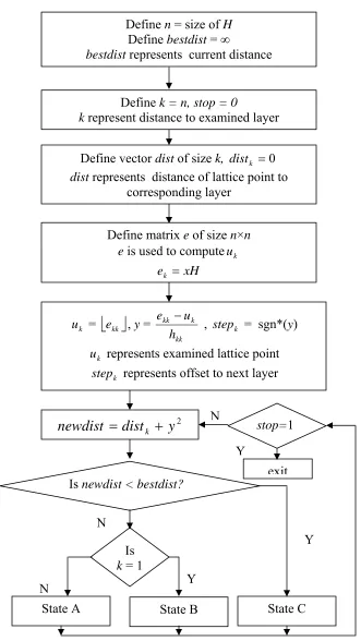
Figure 4.1 Flow Chart of Decoding Algorithm Define n = size of H
Define bestdist = ∞
bestdist represents current distance
Define k = n, stop = 0
k represent distance to examined layer
Define vector dist of size k, distk =0
dist represents distance of lattice point to corresponding layer
Define matrix e of size n×n e is used to computeuk
xH ek =
k
u =
⎣ ⎦
ekk , y = kkk kk
h u e −
, stepk = sgn*(y)
k
u represents examined lattice point
k
step represents offset to next layer
2
y
dist
newdist
=
k+
State A State B State C
Y Is newdist < bestdist?
Is k = 1
N
N
stop=1 N
Y
Y
Figure 4.2 Flow Chart of State A of Decoding Algorithm
Figure 4.3 Flow Chart of State B of Decoding Algorithm
ki ki i
k e yh
e −1, = − for i = 1,….k - 1
k = k – 1
k
u =
ekk ,distk =newdisty =
kk k kk
h u e −
, stepk = sgn*(y)
u
u)= , k = k +1 bestdist = newdist
k
u = uk +stepk, y =
kk k kk
h u e −
stepk = −stepk +sgn* (stepk)
State B
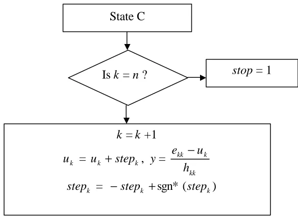
Figure 4.4 Flow Chart of State C of Decoding Algorithm
In this algorithm, k is the dimension of the sublayer structure that is currently being
investigated. In state A this algorithm performs three steps:
1. finding k – dimensional layer
2. finding distance to layer
3. after finding distance expand layer into ( k -1)
State B is invoked when the algorithm has successfully moved down all the way to
the zero-dimensional layer (that is, a lattice point) without exceeding the lowest distance.
In this state this algorithm store lattice point as output and update the lowest distance.
State C is invoked when distance to examined layer is greater than lowest
distance. In this state this algorithm checks condition to stop the search. If condition to
stop is not meet than it moves up one step in hierarchy of layer. Is k = n ?
k = k +1
k
u = uk +stepk, y =
kk k kk
h u e −
stepk = −stepk +sgn* (stepk)
stop = 1
The operation sgn*(z) returns:
sgn*(z) = -1 if z = 0
= 1 if z > 0
[z] = integer closet to z i.e. [2.4] = 2 and [2.6] = 3
In hardware [z] can be implemented in following way.
Suppose z is amplified by p wherep =2S. If S -1 bit of z is 0 then reset S-1 to 0 bits of z
as zeros. If S -1 bit z is 1 thenp =2S. If S -1 bit of z is 1 then reset S-1 to 0 bits of z as
zeros and add S
2 to z.
4.2 A geometric view of the square root
There are two facts concerning the square of an integer that are useful in the
inverse process of finding the square root. The first concerns the number of digits.
If 0 < a < 10 then 0 < a2 < 100,
if 10 < a < 100 then 100 < a2 < 10 000,
if 100 < a < 1000 then 10 000 < a2 < 1 000000,
and so on.
The point to see here is that the square of an integer has either twice as many digits as the
integer itself, or one less than twice as many. So, since 9,409 has 4 digits its square root
has 2 digits, and the square root of the 13 digit number 3,871,696,594,290 has 7 digits.
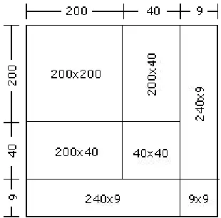
The second fact concerns the "geometry" of squaring a number. Consider, for example,
the square of 249 so the geometric object to consider is a square with side of length 249
Figure 4.5 Geometric view of the square of three digit number
The square of 249 is 200x200 + 2(200x40) + 40x40 + 2(240x9) + 9x9 = 62001.
Now to find the square root of an integer you need first to determine the number of digits
there will be. Let us find the square root of 64 009. Since 64 009 has 5 digits, the square
root of 64009 will have 3 digits. A square of a 3 digit number is divided into 7 parts as
shown in the diagram.
Figure 4.6 Geometric view of the square of three digit number 1
3
6 2
4
5
To find the square root of 64009 divide the number in group of
“two” as 6 | 40 | 09 and start with the group of digits nearest to
the left (in this case 6). This represents the square of a. We know
that the largest perfect square less that 6 is 4, and that the square
root of 4 is 2. Since 2 must be placed in the hundreds position,
we can say a = 2*100. The area of region 1 is 200x200 = 40 000.
We then subtract this area from the total area of 64 009. By
looking at the diagram we realize that next we should remove the
areas of the two regions whose sides are a and b (region 2 and 3).
To find the length of b we must estimate the quotient of 24 009
by 400. The 400 is arrived at by recalling that two regions, each
of which has a length of 200, would have an overall length of
2(200) = 400.
The quotient of 24 009 by 400 is approximately 60. However looking again at our
diagram we realize that besides region2 and 3, we also must subtract an area of b x b
(region 4). Since 2 x 200 x 60 = 24 000 we are left with only 9, but we need to subtract b
x b which is 60 x 60 = 3 600. Thus we reduce our estimate of b to 50, and place a 5 in the
tens position of the square root calculation. Two rectangles (region 2 and 3), each 200
units by 50 units, have a total area of 20 000 square units. Subtracting 20 000 from 24
009 leaves 4 009. Again, going back to the diagram we note that the area (region 4) of b x
b that must be subtracted is now 50 x 50 = 2 500. Subtracting 2 500 from 4 009 leaves 1
Returning to the diagram we note that next we must subtract the areas of the two regions
which has a length of a + b = 250 units each. The unknown quantity c can now be
estimated by the quotient of 1 509 by 500. 500 is arrived by placing the two regions
together to arrive at a rectangle with length 2 x 250 = 500. The quotient of 1 509 by 500
is approximately 3. Place 3 in the units position of the square root calculation and
subtract the sum of the areas of regions 5 and 6 , which is 2 x 250 x 3 = 1 500.
Subtracting 1 500 from 1 509 leaves 9. From the diagram the region 7 is the only region
not subtracted so far and its area is c x c = 3 x 3 = 9. Subtracting 9 from our previous
remainder leaves us with a remainder of 0. Thus the square root of 64009 is 253.
The Square root Algorithm:
Input: a positive integer x.
Output:root = x rounded toward zero.
figure continued on next page w = [1, 10,100………]
w represents weight associated with number
Divide number x into groups of two d = no of digits in root ( no of groups)
i = d-1 i is used index of w
Find p such that p = first group ( left most)
p represents perfect square q = SQRT ( p )
figure continued on next page
Is d = 1? root = q
EXIT Y
i w q root = ×
2
root x n= −
N A
i = i - 1 2
× =root add
quotient = round ( n – add ) quotient = round( quotient -wi)×wi
Is quotient = 0?
done = 1 done = 0
Y N
Is done = 0?
) )
((add quotient quotient2 n
m= − × +
Is m = 0
done = 1 n = m
root = root + quotient N
i w quotient
quotient = −
N
Y
B Y
Figure 4.7 Flow Chart of Square root Algorithm
In this algorithm we need to find number of digits (d) in square root of given number (x).
This can be implemented as follow:
d = 2 if 0 ≤x≤ 99
d = 3 if 100 ≤x≤ 9999
d = 4 if 10000 ≤x≤ 999999
………
The function SQRT ( p ) in above algorithm returns q as follow:
q = 9 if p > 80
q = 8 if p > 63 and p≤ 80
q = 7 if p > 47 and p≤ 63
q = 6 if p > 35 and p≤ 47
q = 5 if p > 24 and p≤ 35
B
d = d -1
Is d≥ 1 C
returnrootand exit Y
q = 4 if p > 15 and p = 24
q = 3 if p > 8 and p = 15
q = 2 if p > 3 and p = 8
q = 1 if p > 0 and p = 3
q = 0 if p = 0
4.3 Strassen Matrix Inversion Method
Suppose matrix C is the inverse of matrix A. If the size of A is N×N, the size of C
is also N×N. In Strassen method the matrix A is divided into four sub matrix A11, A12,
A21 , A22 in such way that number of rows in A11 equal to number of columns in A21 .
A =
21 11 A A 22 12 A A
and C =
21 11 C C 22 12 C C
Let A =
NN P N NM N PN PP PM P MN MP MM M N P M a a a a a a a a a a a a a a a a .. .. .. .. .. .. .. .. .. .. .. .. .. .. .. .. .. .. .. .. 1 1 1 1 1 1 11
A11, A12, A21 , A22 given by
A11 =
MM M M a a a a .. .. .. .. .. 1 1 11
A12 =
MN MP N P a a a a .. .. .. .. .. 1 1
A21 =
NM N M P P a a a a .. .. .. .. .. 1 1
A22 =
where M = 2
N
if N = even
M = round
2
N
if N = odd
P = M + 1
Strassen Matrix Inversion Algorithm:
Input: N×N matrix A
Output: N×N matrix C such that C = A−1
figure continued on next page Divide A into four sub matrix
A11, A12, A21 , A22
R1 = A11−1
R2 = A21×R1
R3 = R1×A12
R4 = A21×R3
R5 = R4−A22
Figure 4.8 Flow Chart of Strassen Matrix InversionAlgorithm R6 = R5−1
6 3
12 R R
C = ×
2 6
21 R R
C = ×
21
3
7 R C
R = ×
7 1
11 R R
C = −
6
22 R
4.3.1 Reduction of Strassen Matrix Inversion algorithm for 4 × 4 lower triangular
matrix
If matrix is lower triangular, it’s inverse is also lower triangular. Let A and C are
inverses of each other.
A =
44 43 42 41 33 32 31 22 21 11 0 0 0 0 0 0 a a a a a a a a a a
C =
44 43 42 41 33 32 31 22 21 11 0 0 0 0 0 0 c c c c c c c c c c
A11 =
2 2 21 11 0 a a a
A12 =
0 0 0 0
A21 =
2 4 41 32 31 a a a a
A22 =
44 43 33 0 a a a
1) R1= A11−1
R1 = 1 1
d
− 21 11 22 0
a a a
where d1=a11∗a22
2) R2 = A21× R1
R2 =
2 4 41 32 31 a a a a × 1 1
d
− 21 11 22 0
a a a
R2 = 1 1
d
2 2 21 12 11 r r r r where 11 42 22 21 2 4 22 41 21 11 32 12 21 32 22 32 11 * * * * * * a a r a a a a r a a r a a a a r = − = = − =
3) R3 = 0 (Qa12 =0)
5) R5 = - A22 (QR4=0) = − − − 44 43 33 0 a a a
6) R6=R5−1
= 2 1
d
− − 33 43 44 0 a a a
where d2 =a33∗a44
7) C12 = 0 (QR3=0)
8) C21 = R6 × R2
C21 = 2 1
d
− − 33 43 44 0 a a a × 1 1
d
2 2 21 12 11 r r r r = 1 * 2 1 d
d
22 21 12 11 h h h h where 22 33 12 43 22 21 3 3 11 43 21 12 44 12 11 44 11 * * * * * * r a r a h r a r a h r a h r a h − = − = − = − =
9) R7 = 0 (QR3=0)
10)C11 = R1 (QR7=0)
C11 = 1 1
d
− 21 11 22 0
a a a
11)C22 = - R6
C22 = 2 1
d
− − 33 43 44 0 a a a
The inverse C of 4×4 lower triangular matrix A is given by
C =
C = − − − 2 2 2 * 1 2 * 1 0 2 2 * 1 2 * 1 0 0 1 1 0 0 0 1 33 43 22 21 44 12 11 11 21 22 d a d a d d h d d h d a d d h d d h d a d a d a
where d1=a11∗a22
d2 =a33∗a44
h11 =−a44∗r11
h12 =−a44∗r12
h21 =a43∗r11−a33*r21
h22 =a43∗r12 −a33*r22
r11 =a32*a22 −a32*a21
r12 =a32*a11
r21=a41*a22 −a42*a21
r22=a42∗a11
4.4 QR decomposition of matrix
The matrix A can be decomposed into A=QR
Here R is upper triangular matrix, while Q is orthogonal matrix, that is, QQT= I w here
T
Q is the transpose matrix of Q. The standard algorithm for the QR decomposition
applied to a given matrix can zero all elements in a column of the matrix situated below a
chosen element. Thus we arrange for the first Householder matrix Q1 to zero all elements
in the first column of A below the first element. Similarly Q2 zeroes all elements in the
second column below the second element, and so on up to Qn−1Thus
A Q Q
R= n−1... 1
(
)
1 11 1
1... ... −
−
− =
= Qn Q Q Qn Q
4.4.1 Householder Matrix
The Householder transformation is often described in terms of multiplication by a
matrix known as Householder matrix. A Householder matrix has the form
T WW I
H = −2 where W is a column vector. The formation of the Householder matrix to
reduce to zero a vector X from position k to position n is summarized in the following
algorithm:
Given an n-dimensional vector X and an index k such that 1≤k ≤n−1 find a vector
W so that the matrix H =I−2WWTreduces positions k+1,…, n of vector X to zero, so
the vector HX has the form
[
Z1,Z2...ZK,0,0,...0]
T1. Set Wi = 0 for i =1,…,k-1.
2. Find g= Xk2 +...Xn2
3. Find s= 2g(g+ Xk )
4. Set
s
g X X
5. Set
s X
Wi = i for i = k+1,…,n
QR Decomposition Algorithm:
Input: ann× n matrix A
Output: n× n upper triangular matrix R and n× n orthogonal matrix Q.
figure continued on next page k = 1, B = A, R = 0
mx = MAX( Akk,A(k+1)k,....Ank) BB
mx A A
Akk, (k+1)k.... nk
2 2
) 1 ( 2
... nk
k k
kk A A
A
Sum= + +
AA
=
S SIGN( Sum,Akk)
kk
kk S A
A = +
kk
k S A
C = ×
AA
j = k + 1
nj nk j
k k k kj
kkA A A A A
A
S1= + ( +1) ( +1) +....
k C
S T = 1
pk pj
pk A T A
A = − ×
p varies from k to n
1 − = j j
Is j= n ?
1
− =k k
Is k< n ? BB
CC Y
N
Y
N
Figure 4.9 Flow Chart of QR Decomposition Algorithm
In the above algorithm operation MAX(p1,p2...pn) finds absolute value of
p1,p2...pn and then return maximum absolute value e.g. MAX (-2.1 ,1.0) returns 2.1.
The operation SIGN ( M, N) returns y as follow:
y = M if N > 0
y = -M if N < 0
N Y
i
ii d
R = , x = 1 i varies from 1 to n
xy
xy A
R =
y varies from x + 1 to n
x = x + 1
Is x = n ?
N Y
CC
Q = BR−1
Chapter 5
Prototyping of Closest Point Search Algorithm
This chapter explains how to prototype the closest point search algorithm on the
Altera system-on-chip (Stratix EP1S10F780C6).
5.1 Why system-on-chip
The MIMO prototyping is challenging because of the complexity of the system.
The large complexity of AV algorithms needs to be partition over DSP and FPGAs. It
also requires the presence of interface drivers to support intercommunication between
DSP, FPGAs. By using system-on-chip we can develop microprocessor based system,
hardware logic and driver to communicate between microprocessor based system and
hardware logic on the same chip. The main goal is to develop a platform for parallel
execution of the preprocessing unit and the lattice decoder, therefore improving the
overall performance and decoding rate (Mbps) of the MIMO channel decoder.
5.2 Prototyping Closest Point Search Algorithm
We can divide the closest point search algorithm into two parts 1) preprocessing
and 2) decoding. Preprocessing contains QR decomposition of channel matrix and matrix
QR involves operations like finding square-root, floating point multiplication,
division. FPGAs are not suitable for QR decomposition and matrix inversion. These
operations are performed by using NIOS embedded processor in the FPGA.
If we analysis AV algorithm in details, it is found that there are three different
states A, B, C. For given k (layer index) state A performs calculations for k-1 layer, while
states B, C perform calculations for layer k. It means that data for state B and C are not
depended on data from state A. Because search procedure can jump to either state B or C
after performing sate A and no data dependency of state B, C on state A, we can start
state B and C in parallel with state A. We can accept or reject the output from state B or
C depending on result of state A. If current state is C, we can start another state C in
parallel with first state C. Depending on the result of first C; we can accept or reject the
output of second state C.
Such parallelism cannot be achieved by using microprocessor so we use FPGAs
to model decoder. The following diagram shows architecture of closest point search
algorithm.
Figure 5.1 Hardware architecture of lattice decoder
NIOS
Microprocessor
Based System
Hardware
Controller
State A
State B
State C
ready
send
data
Controller is the most important part of the lattice decoder. It is used to control data
between State A, B, C and NIOS microprocessor based system.
5.2.1 Interface between Nios microprocessor based system and
Controller
Figure 5.2 Interface between Controller and NIOS Microprocessor Based System
C code for NIOS System VHDL code for Controller
……. …….
…… ……..
Loop: process( ready)
“ Put data on bus”
“ Activate ready signal” “ read data”
“ Wait for send signal” “ activate send signal”
“ Go to loop” …..
End Loop; end process; ready
send
data
Controller
Nios
NIOS microprocessor based system computes QR and R inversion and transfer Q and R
matrix to the controller. NIOS microprocessor based system transfer one row of Q and R
matrix at a time. When it is ready to transfer the data, it activates the ready signal. This
ready signal is in sensitivity list of process of controller so it triggers the process. The
process in controller read the data and activate send signal. The send signal is used to
interrupt the NIOS microprocessor based system so that it can send next data.
5.2.2 Interface between State A, B, C and Controller
Figure 5.3 Interface between Controller and State A, B, C Start A
Ready Data
Controller
start BReady
Data
Start C1
Ready Data Start C2
Ready
Data Start
State A
ReadyData
Start
State B
ReadyData
Start
State C1
ReadyData
Start
State C2
Ready5.2.3 VHDL Code Structure of Controller for Interface with State A, B, C:
architecture of controller is
k := n
CURRENT_STATE <= A
STATE_CHANGE <= ‘0’
………
……….
begin
P1: process ( CURRENT_STATE)
begin
If ( CURRENT_STATE = A) then
“put data on bus for state A, B, C1 and start them”
“wait for result from state A”
“store data from state A “
“from result of state A check what is next state after A”
“store or discard result form B, C1 depending on state A”
end if
If ( CURRENT_STATE = C) then
“put data on bus for state C1, C2 and start them”
“wait for result from state C1”
“store data from state C1 “
“from result of state C1 check what is next state after C1”
end if
STATE_CHANGE <= ‘1’
end process P1
P2: process (STATE_CHANGE)
begin
if ( new distance < best distance ) then
CURRENT_STATE <= A
else
CURRENT_STATE <= C
end if
end process P2
end architecture
Chapter 6
Results
This chapter gives the experimental results obtained for both the preprocessing
and decoding part of the MIMO decoder.
6.1 Results of Pre-processing Part
The pre-processing part is executed on Nios microprocessor based system which
runs at frequency of 50MHz on the Stratix EP1S10F780C6 device. Using the Division
custom instruction, the maximum frequency is 50MHz.
6.1.1 Results of Division
The table 6.1 compares number of clock cycles required to perform division using
Nios microprocessor without hardware divider and with hardware divider. Nios
a b c = a ÷ b Number of cycles
With divider 31,111 1,000 31 38
With divider -31,111 1,000 -31 40
Without divider 31,111 1,000 31 65
Without divider -31,111 1,000 -31 69
Table 6.1 Comparison of Nios Processor with & without divider to perform division
Table 6.1 clearly shows division is 1.6.times faster on Nios microprocessor with divider
than on Nios microprocessor with divider.
6.1.2 Results of Square root
The table 6.2 compares number of clock cycles required to find square root of
integer (rounded toward zero) using square root algorithm explained in 3.2 and C
language “sqrt “function.
A Round( a) Number of cycles using C
language “sqrt” function
Number of cycles using
square root algorithm
99 9 6,192 51
999 31 5,870 521
6,420 80 6,015 396
6,40,094 800 5,759 550
The table 6.2 shows that square root algorithm explained 4.2 in is faster than “sqrt” C
language function. The reason is that “sqrt” function uses floating point operation
(execution of floating point operation on Nios fixed point processor takes more cycles)
and squa re root algorithm explained in 4.2 uses hardware multiplier and divider.
6.1.3 Results of Strassen Matrix Inversion Method
The table 6.3 shows number of cycles required to invert 4×4 and 8×8 lower
triangular matrix using Strassen method. It clearly shows that matrix inversion using
divider is almost 3.5 times faster than inversion without divider.
Matrix size Number of cycles
using hardware divider
Number of cycles
without divider
4×4 873 2,973
8×8 5,755 17,820
Table 6.3 Number of cycles required to invert 4×4 and 8×8 lower triangular matrix
using Strassen method
6.1.4 Results of QR Decomposition of matrix
The table 6.4 shows number of cycles required to perform QR decomposition of
4×4 matrix. It shows that use of divider, square root algorithm speed up QR
Matrix size Number of cycles
with multiplier
only
Number of cycles
with multiplier and
divider
Number of cycles
with multiplier, divider
and square root algorithm
4×4 26,508 19,307 6,929
Table 6.4 Number of cycles required to perform QR decomposition of 4×4 matrix
6.1.5 Results of preprocessing part
The table 6.5 shows number cycles required to perform pre processing part of
decoding
Matrix size Number of cycles
4×4 9,736
8×8 36,587
Table 6.5 Number of cycles required to perform pre processing part of decoding
6.2 Results of Decoding Part
State A, B, C of decoder and controller to controller parallelism of A, B, C are
developed using VHDL and simulated using Aldec simulator. 18 clock cycles are
required to complete state A and 9 clocks cycles are required to complete both state B
and C. The matlab and C version of decoder are also developed. The result from matlab
In order to test decoder we assumed received signal is [-1,-3, 1, 1] and channel
matrix H some random number
− − − − − − − − − = 4070 . 0 3665 . 1 9414 . 2 0963 . 0 7477 . 0 4380 . 0 8866 . 1 5484 . 0 0893 . 0 1918 . 1 7284 . 0 2656 . 0 8727 . 0 9800 . 0 3807 . 1 9794 . 0 H
Given an example, we set up the SNR as 20db. In this case, the number of iterations to
perform search operation in Matlab is 9 and search procedure goes through following
sequence of states.
Iteration 1 2 3 4 5 6 7 8 9
State A A A B A C C C C
Table 6.6 Sequence of state in matlab
Iteration 1 2 3 4 5 6
State A A A A C C
Parallel state B C C
Table 6.7 Sequence of state in VHDL
In VHDL we can start two states at the same time so in iteration 3 states A and B
are executed at the same time, similarly in iteration 4 state A and C, in iteration 5 states A
If we consider that all state executes in sequence instead of parallel like matlab, than total
number of cycles required to complete search operation for this case are as follow:
18 × 4 (number of times A come) + 9 × 1 (number of times B come) +
9×3 (number of times C come – 1) + 2 (number of cycles for last C) = 110 cycles
Total number of cycles to complete search operation if states are executed in parallel is as
follow:
18 × 4 + 9 × 3 + 2 = 83 cycles
Because of parallelism we can save 110 – 83 = 27 cycles for this case.
The bit rate of decoder is:
(frequency× bits_per_dimension × N ) ÷ (total number of cycles)
N = 4 for 4 - antenna system
bits_per_dimension = 2
Total number of cycles in case of parallel architecture is 83 and maximum frequency is
54 Mhz so bit rate in case of 4.85 Mbits/secons. The sequential decoder takes 3571
cycles on Nios microprocessor based system which runs at 50 Mhz so in this case data