2017 International Conference on Computer, Electronics and Communication Engineering (CECE 2017) ISBN: 978-1-60595-476-9
A Novel Methodology on Optimizing the Performance of
Multi-core Processor Using FPGA
Yue RUAN
Zhejiang Shuren University, Hangzhou, Zhejiang Province, China
Keywords: Performance optimizing, FPGA, Multi-core processor, Scheduling strategy, SoC.
Abstract. With rapid progress in microelectronic technology and higher performance requirements, core processors (MP) have become widely used in various applications. Among them, multi-processor System-on-Chip (MPSoC) received focus because of its high integration level and low power solution. This work proposed more efficient way to implement MPSoC with higher performance. Synchronous data flow (SDF) is used to model high-speed MPSoC systems, and to simulate the system level functional algorithms. After building a suitable FPGA platform architecture, we prototype these SDF graphs onto FPGA based MPSoC platform. Simulation results show that the MPSoC platform has higher performance than a single processor platform, with novel architecture and scheduling strategy used. Furthermore, different scheduling strategies, including static order and run-time order, are compared on MPSoC. The results have shown that the optimized static order strategy can achieve higher performance than run-time order strategy, with less buffer cost.
Introduction
As the rapid progress of microelectronic technology nowadays, it is making the integration of a large number of processors on a single chip possible, the multiprocessor System-on-Chip(MPSoC) architecture becomes popular in recent years. For example, SoC used in smart-phones often have 4 to 8 processing cores based on ARM cortex series. CPUs and GPUs on desktop/laptop have even more cores or computing units on single chip. The key feature of these multi-core systems is that processors can cooperate on distributed processing tasks in the same multiprocessor computing systems. Each processor is operated in a "compatible" mode in the same system, but they have their own relative independent responsibility. Communicate between processors should be done through the internal structure when it is needed. The transmission delay between processors should be compressed to as small as possible. Designing reasonable support structures and taking exploration to find the best-suit architecture for the target design domain are the key issues to make processors working in an efficient way.
MPSoC architectures have many advantages in the modern electronic system. Compared to the traditional single processor system which MPSoC system replaces, MPSoC systems are easier to guarantee the real time performance and have higher computation capability, because of their natural parallel feature. There are many on-chip buses between processing cores to increase throughput and decrease the transmission delay. Heterogeneous processors could optimize energy and area efficiency due to their special purposed design. As we can see from ARM’s application processors, two different cores are used, one is computing intensified, the other is low power and used in lightweight applications, and they are combined together which ARM calls it big-LITTLE architecture. These can cause less power consumption and competitive cost for application products. Besides the above, single-chip-solution systems have integrated all or most of the electronic system into a same chip, so fewer packages are needed, and assembly costs are reduced as well.
encoding, decoding and radio interface. An audio processor can be used for music playback. One or more image signal processors (ISP) are used for camera and video-on-phone capability. Besides these, other embedded processors can also be integrated for other functions, which are traditionally designed as dedicated blocks. The left part of this paper is organized as the following:
Section 2 introduces the background of Synchronous data flow (SDF) models and describes the functions of communication assistant (CA), together with its internal task logic, interface specifications and software drivers. In section 3, the architecture of our MPSoC hardware platform is proposed. All the interconnections of on chip components in tile based MPSoC platform and dual port software FIFO are described. In section 4, two specific SDF applications are implemented on the proposed MPSoC platform. Different scheduling strategies are used for these two applications. The same applications are also implemented on single core platform in order to compare its performance with MPSoC. From the comparisons we can find out the differences in performance between single core and MPSoC.
SDF Model and Communication Assistant
SDF Model and SDF Graph
An example of a synchronous data flow is depicted in Figure 1. This SDF graph consists of three nodes and two arcs. The nodes in this graph represent operations, which are called processes. These processes are computed by reading tokens from their input ports, and write the results of the computation as tokens on the output ports. An essential property of SDF graphs is that every time if a process fire (performs a computation) it consumes the same amount of tokens from its input ports and produces the same amount of tokens on its output ports. These numbers of data samples produced or consumed by each node on each invocation is specified as a fix number by designers even before the execute start. Furthermore, we define these amounts to be called the rates of the ports, and are visualized as port annotations in Figure 1 (N1,2; M1,2; N2,3; M2,3).
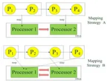
Processes can be implemented as software functions, which can complete a relative isolated task. Every processor can contain more than one process according to its feature. Designers should decide how to put processes into processors before the executing begin. Different ways to map processes could lead to different performance results. To illustrate different mapping strategies, we put a 4-process SDF application into a two-processor MPSoC platform. Two different mapping strategies are used in this application. Strategy A puts P1 and P2 into processor 1, P3 and P4 into processor 2. Strategy B puts P1 and P4 into processor 1, P2 and P3 into processor 2. Figure 2 below shows the implementation of a 4-process pipelined SDF application into a 2-processor platform with different mapping strategies.
[image:2.612.368.473.528.608.2]
Figure 1. An SDF graph. Figure 2. Different mapping strategies using SDF.
Figure 3. Simulation of 4-process by different mapping strategies.
[image:2.612.242.369.645.699.2]mapping strategies could impact the efficiency of dataflow. Besides the throughput, these two mapping strategies also need the different communication mechanism between processors for the hardware platform. In strategy A, processor 1 send data tokens to processor 2 in a unidirectional way. So only one hardware inter-processor FIFO is needed. In strategy B, both processors need to send and receive data tokens. This means data tokens are transferring in a bidirectional way during executing time. Two FIFOs in different directions are needed between processors.
In order to simplify the conditions, we suppose all the data tokens produced or consumed in each process is one, FIFO storage in all channel is one and use static order scheduling to schedule. The executing sequence of processes in two mapping strategies can be simulated in Figure 3. It is easy to figure out the first mapping strategy can achieve higher throughput, since it doesn’t have idle waiting executing cycles.
Communication Assistant
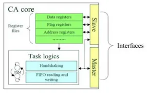
Communication assistant (CA) is a customized IP core which is needed in our prototype. It is a hardware peripheral used to support data transmission between processors. The main usage of CA is transmitting data tokens between software FIFOs, which belongs to different processors. A CA consists of two parts. Either of them is responsible for reading or writing operations. Depend on sending data or receiving data, we call them CA sending logic and CA receiving logic. Figure 4 shows the basic function of CA. Figure 5 illustrates the block diagram of CA.
[image:3.612.373.524.313.416.2]
Figure 4. Basic function of CA. Figure 5. Block diagram of CA.
As shown in the figure above, a CA consists of functional registers, task logic and interfaces. Task logic is used to carry out CA’s main functions. It controls the logic behaviors of CA, such as control data communication with the FIFO and handshaking with other CAs. Interfaces are the windows of CA to communicate with other on chip components by internal buses. They follow Avalon-MM standards and have master and slave two kinds of ports. Functional registers can be used to store lots important information for CA. They also could be accessed by other on chip components and provide information for internal logics at the same time.
Proposed Multi-processor SoC Architecture
Framework of Tile-based MPSoC
Figure 6. A tile based MPSoC architecture.
[image:4.612.213.400.238.433.2]Detailed Structure of Tiles
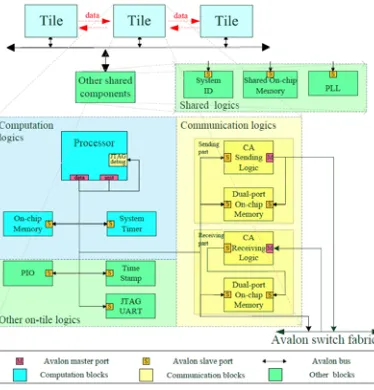
Figure 7 below shows the detailed architecture in a tile we proposed. All the tiles have the similar structure, which means they can be reused for different streaming applications with minor changes. Every tile contains computation logics, communication logics, and other logics. The interconnections between all on chip components are done by Altera’s Avalon switch fabric.
Figure 7. Detailed structure of a tile.
Dedicated on-chip Memory
Shared memory can be used as the program memory for different processors in MPSoC system. One of the shared memory examples is using SDRAM. It has large storage space, processors can execute their software in the different address offset without any interference with each other. However, the main problem is contention will happen when processors want to access the same port, and this will have bad effect for synchronization of processors and the scalability of the system.
[image:4.612.192.424.641.706.2]To solve this problem, we use the dedicated memory structure for our platform, that means one on chip memory has to be dedicated corresponding to one processor in the same tile. According to Avalon switch fabric’s slave side arbitration rule, processor access its on-tile on chip program memory with a special path, when data communication begins, processor only access on chip memory instead of holding the bus. All processors and memory are linked to same Avalon switch fabric, but no interferes and contention would happen when the processor executing its own tasks. Figure 8 shows the difference between dedicated memory and shared memory.
Figure 9. The structure of circular FIFO used in software.
Software FIFO
As we mentioned before, FIFOs are used as the interconnection structure between processes in SDF application. In our proposed architecture, when processes are mapped to the same processor, software FIFOs are used as the only interconnection to transfer data tokens between them. When processes are mapped to different processors, data transferring will be done by CA and FIFO together. Figure 9 below shows the structure of circular FIFO used in software.
As shown in Figure 9, software FIFO is used to transfer data tokens between two processes. All the data tokens would be written into the tail and read from head. The maximum number of data this FIFO can store is limited, and it is defined by the designers before the executing time. Besides the separated data storage space in program memory, it contains other key parameters include head pointer, tail pointer, base address, and FIFO size, which are all necessary for a FIFO. These parameters are stored in a fixed address in program memory. So the processor and CA can easily locate and updates these parameters during the executing phase. This software FIFO uses circular FIFO structure. The pointers are moving in one direction in circular, the number of data tokens stored in FIFO can be calculated by the difference of these two parameters. Designers have to sacrifice one unit memory to distinguish full or empty of storage space. So the really FIFO storage size should be one unit smaller than the size storage space occupied in the memory.
Simulation and Results
In specific SDF applications, different processes are mapped to several processors by assignment rules. The executing orders of these processes are decided by schedulers. These scheduling decisions can happen either in run time or compile time.
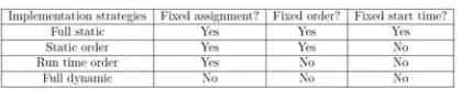
Taking these decisions during executing time of SDF jobs could lead some run time overhead because processors have to check whether target processes are ready for executing at run time. However, this overhead time can be reduced by making decisions before executing jobs (at compile time). If the schedule decision can be taken at run time, it is also more flexible. Designers don’t need to think about if these processes should be available at a certain time. In a multi-processor system, it is too hard to calculate these. Therefore, scheduling strategy should be selected to depend on the real situation. Four implementation strategies are illustrated in table 1.
Table 1. Comparison of scheduling strategies.
We use Altera’s Stratix II FPGA multiprocessor as the hardware platform. Because of this, full static and full dynamic scheduling strategies are very hard to implement. So we only focus on static order and run time order strategies in our platform. The following figure shows the scheduling latency model of mapping a 4-stage pipelined application onto a 2-core based MPSoC platform.
[image:5.612.203.413.619.660.2]on the inter-tile channel is decomposed into two on-tile buffer and FIFOδ,3. So we use Pδ this
process to simulate the delay time caused by CA transferring data in the system latency model. However, this Pδ is a very short latency process, and it is the only several crystal oscillator cycle.
This makes it much shorter than other processes in this SDF application, which is measured by software instruction cycle. The parameters Ni,j , Mi,j in this figure represent the number of tokens should send or receive for the FIFO when the target process executes. They are all decided when the SDF application is built except M2,δ , Nδ,3 are constantly equal to 1. Because CA only transfer one tokes from FIFO2,δ to FIFOδ,3 when Pδ executes.
We can also abstract these logics into algorithms and show them in figure 11 below. Bij represents the function used to calculate data tokens in FIFOij , and γij represent the size of FIFOij .
[image:6.612.273.524.203.316.2]
Figure 10. Scheduling latency model Figure 11. Algorithms of static order of a specific application. and run time order.
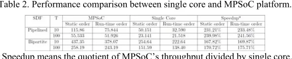
In order to evaluate the performance of MPSoC platform compared with single core, some experiments are implemented onto the single core platform with similar sequential software.The results are shown in Table 2 below.
Table 2. Performance comparison between single core and MPSoC platform.
a Speedup means the quotient of MPSoC’s throughput divided by single core.
Table 2 above gives a brief performance comparison between a single core platform and an MPSoC platform in different scheduling strategies conditions. When the latency factor (T) is equal to 100, the speedup of MPSoC platform can achieve 239.91% and 241.31% throughput in 6-process pipelined SDF application, with 170.71% and 175.71% throughput in 4-processes bipartite application. MPSoC platforms show higher performance than single core platforms in this experiment.
Conclusions
In this paper, we build our FPGA based MPSoC, and prototype our SDF applications on them successfully. In order to make our platform match the features of SDF, we optimized the communication mechanism by developing our CA, which is responsible for the data transmission between processors. With this mechanism, we separate the computation and communication parts of our platforms, so processors can just focus on computation. Besides this, dual port on chip FIFOs are used in order to support CA for data transmissions between tiles. Its dual-port features avoid the data contending problem for two master peripherals. Dedicated on chip memories are used for every processor in our platforms.
[image:6.612.163.451.399.458.2]strategies in our platforms. Because of the feature of these scheduling strategies, we choose run time order and static order scheduling strategy in our experiments. Either of these two strategies has their own advantages. We compare and list the throughput of these strategies in different conditions. Finally, we conclude the static order strategy is always better than run time strategy. The difference is obvious when the delay factor is small. Besides this, same applications are also mapped to single core platforms, and the experiment results show that MPSoC platforms perform better than single core platforms.
References
[1]Song Pan, Jiye Huang, Guodong Wang, “Modern DSP Technology” Xi’an Electronic Science & Technology University Press.
[2]Puccinelli, D.; Haenggi, M., “Wireless sensor networks: applications and challenges of ubiquitous sensing,” Circuits and Systems Magazine, IEEE, Vol.5, Issue 3, 2005.
[3]Ruan Yue, Tang Ying, “A water quality monitoring system based on wireless sensor network and solar power supply”, IEEE International Conference on Cyber technology in Automation, Control and Intelligent systems, pp. 126-129, March 2011.
[4]Ruan Yue, Yao Wenji, “Design and Implementation of a SoC-based single chip radio transceiver,” The 7th IEEE International Conference on Wireless Communications, Network and Mobile Computing, vol. 2, pp. 1113-1116, September 2011.
[5]Tang Ying, Ruan Yue, “Research on a Novel Synchronization and Detection Scheme used in Energy Detection UWB Receiver”, The 11th IEEE International Symposium on Communications and Information Technologies (ISCIT 2011), pp 109-113, October 2011.
[6]Altera Corporation: SOPC Builder DataSheet.2003. Available:
http://www.altera.ru/Disks/Altera%20Documentation%20Library/literature/ds/ds_sopc.pdf. [7]Altera Corporation: Nios II software developer's handbook. 2005. Available: