N A N O E X P R E S S
Open Access
Impact of device size and thickness of Al
2
O
3
film
on the Cu pillar and resistive switching
characteristics for 3D cross-point memory
application
Rajeswar Panja, Sourav Roy, Debanjan Jana and Siddheswar Maikap
*Abstract
Impact of the device size and thickness of Al2O3film on the Cu pillars and resistive switching memory characteristics of the Al/Cu/Al2O3/TiN structures have been investigated for the first time. The memory device size and thickness of Al2O3 of 18 nm are observed by transmission electron microscope image. The 20-nm-thick Al2O3films have been used for the Cu pillar formation (i.e., stronger Cu filaments) in the Al/Cu/Al2O3/TiN structures, which can be used for three-dimensional (3D) cross-point architecture as reported previously Nanoscale Res. Lett.9:366, 2014. Fifty randomly picked devices with sizes ranging from 8 × 8 to 0.4 × 0.4μm2have been measured. The 8-μm devices show 100% yield of Cu pillars, whereas only 74% successful is observed for the 0.4-μm devices, because smaller size devices have higher Joule heating effect and larger size devices show long read endurance of 105cycles at a high read voltage of−1.5 V. On the other hand, the resistive switching memory characteristics of the 0.4-μm devices with a 2-nm-thick Al2O3film show superior as compared to those of both the larger device sizes and thicker (10 nm) Al2O3film, owing to higher Cu diffusion rate for the larger size and thicker Al2O3film. In consequence, higher device-to-device uniformity of 88% and lower average RESET current of approximately 328μA are observed for the 0.4-μm devices with a 2-nm-thick Al2O3film. Data retention capability of our memory device of >48 h makes it a promising one for future nanoscale nonvolatile application. This conductive bridging resistive random access memory (CBRAM) device is forming free at a current compliance (CC) of 30μA (even at a lowest CC of 0.1μA) and operation voltage of ±3 V at a high resistance ratio of >104.
Keywords:Resistive switching; Al2O3; Cu pillar; 3D memory; CBRAM
Background
It is known that commercial FLASH memory approaches its scaling limit in sub-20-nm technology node. As it is an alternative solution to replace the FLASH, resistive random access memory (RRAM) becomes a center of attraction to the researchers because of its simple metal-insulator-metal (MIM) structure with low voltage oper-ation (<3 V), high speed operoper-ation, and high scalability potential (<10 nm) [1-5]. Although many switching ma-terials have been reported for the RRAM applications, the Al2O3as a switching material has been reported a few [6-9]. The amorphous Al2O3film has energy gap of 6.2 to 8.8 eV [10,11], dielectric constant of 9 [12], and
Gibbs free energy of −1,582.3 kJ/mole at 300 K [13], which can help to have good resistive switching proper-ties. Wu et al. [6] have described a TiN/Al2O3/Pt RRAM device with a current compliance (CC) of sub-20μA and high operating voltage of +8/−4 V. Wu et al.[14] have re-ported the Al/Al2O3/Pt RRAM devices with an unstable RESET current of 1μA. Lin et al.[7] have reported the re-sistive switching characteristics using a Ti/Al2O3/Pt struc-ture with a high CC of 10 mA and operating voltage of ±3 V. We have reported the resistive switching memory char-acteristics using an IrOx/Al2O3/IrOx-NDs/Al2O3/W struc-ture with a CC/voltage of 500μA/±4 V previously [8]. The resistive switching phenomena using an IrOx/AlOx/W structure with a CC of 200μA in cross-point architecture have been also reported by us [9]. In this regard, many chalcogenide materials in the conductive bridging resistive
* Correspondence:[email protected]
Thin Film Nano Tech. Lab., Department of Electronic Engineering, Chang Gung University, 259 Wen-Hwa 1st Rd., Kwei-Shan, Tao-Yuan 333, Taiwan
random access memory (CBRAM) devices have also been reported by many groups [15-23]. Basically, silver (Ag) or Cu is used as an oxidizing electrode, and the metal ions are migrated through the chalcogenide material under a positive bias on the Ag or Cu electrode. Recently, the AlOx
material in the CBRAM devices using the Ag (or Cu)/ Al2O3/bottom electrode (BE) structures [24-26] has emerged great interest to the researchers due to its high compatibility with the fabrication of conventional CMOS devices. Goux et al. [24] have reported the CBRAM de-vices using a Cu-Te/Al2O3/Si structure at a CC of 5 μA and operating voltage of +0.5/−1 V. In this case, they have used a thin layer (approximately 3 nm) of Al2O3film as an active material and device size was large 1 × 1 mm2. Sleiman et al. [25] have investigated the Cu/AlOx/W
CBRAM devices with a CC of 100 μA and operating voltage of ±2 V. The thickness of AlOx layer is 20 nm,
and a large device size is 1 × 1 mm2. Belmonte et al. [26] have described the resistive switching characteristics in 90-nm Cu/TiW/Al2O3/W 1T1R integrated cell, and they have introduced the TiW as a buffer layer to protect Cu diffusion. In this case, the thickness of Al2O3 layer is 3 nm. The memory device could be operated at 25μA with operation voltage of ±2 V. It is noticed that the Al2O3 ma-terial has been used in the CBRAM devices using bi-layers and different structures and thicknesses. However, impact of device size and thickness of a single Al2O3layer using the Cu/Al2O3/TiN CBRAM devices have not yet been reported.
On the other hand, one of the main challenges of CBRAM is to achieve high device uniformity and inte-gration density. To have high-density memory, conven-tional three-dimensional (3D) FLASH has been conducted through-silicon-via (TSV) [27-30], which acts as intercon-nect in each stack. But one of the bottlenecks of TSV is high cost and large integration area. Joblot et al. [31] have reported the capability of Cu pillar for 3D interconnection technology. So, the conventional TSV technique of 3D FLASH can be also replaced by Cu pillar formation (i.e., stronger Cu filament in CBRAM structure) through 3D cross-point memory architecture for future below 11-nm technology node, which has been demonstrated previously [32]. In this case, each stack of cross-points memory could be connected through Cu pillar which would be a promis-ing way for achievpromis-ing ultra-high-density memory appli-cation. Therefore, the device size-dependent Cu pillar characteristics in the Cu/Al2O3/TiN structures have been also investigated for potential application.
In this study, impact of the device size and thickness on the Cu pillars and resistive switching memory charac-teristics using a single Al2O3layer in the Cu/Al2O3/TiN CBRAM devices has been investigated. The amorphous Al2O3 film with a thickness of 18 nm and the device sizes are observed by transmission electron microscope
(TEM) image. By measuring 50 randomly picked devices, the empirical result tells that large size devices are promising for future Cu pillar applications. From cumula-tive probability of 50 devices, the Cu pillars can reach up to a high CC of 70 mA. Hence, the strong metallic path inside the Al2O3 layer can be used as a connecting way among the different stacks of high-density 3D memory de-vices. Long read endurance of 105cycles of the large size devices at a high read voltage of−1.5 V ensures about the robustness of the Cu pillars or metallic paths. In addition, thickness-dependent resistive switching memory charac-teristics are also observed. Superior CBRAM characteris-tics such as high switching yield of 88%, lower average RESET current of approximately 328 μA, and acceptable resistance ratio of 9.6 are obtained for the 0.4-μm devices with a 2-nm-thick Al2O3film under low voltage of ±2 V, which is due to lower diffusion of Cu ions into the Al2O3 films under external bias. The resistive switching mechan-ism is based on the formation and dissolution of the Cu filaments into the Al2O3films. Good data retention ability of >48 h is also obtained. This CBRAM device shows forming-free current-voltage (I-V) characteristics under a CC of 30μA, even at lowest CC of 0.1μA.
Methods
will be formed under external positive bias on the TE. Other thicknesses of 2 to 10 nm were used to study the re-sistive switching characteristics. Fifty devices for each size and thickness of Al2O3were measured randomly. All the electrical measurements were performed by Agilent 4156C precision semiconductor parameter analyzer (Agilent Technologies, Inc., Santa Clara, CA, USA).
[image:3.595.56.291.266.686.2]Results and discussion
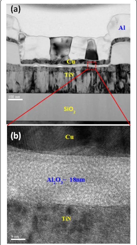
Figure 1a shows TEM image of an Al/Cu/Al2O3/TiN via-hole device. All layers are observed clearly. The device size of approximately 0.5 × 0.5μm2is observed. Figure 1b shows high-resolution TEM image inside the via-hole region. The thickness of Al2O3 layer is approximately
18 nm, including a thin TiOxNylayer on the TiN surface.
This Al2O3 film shows amorphous. Due to the thicker Al2O3film, the stronger Cu filament (or pillar) could be formed inside the via-hole region for 3D cross-point memory application, which has been discussed below.
[image:3.595.304.538.309.665.2]The I-Vcharacteristics of randomly measured 50 pris-tine devices with two different sizes viz. 8 × 8 and 0.4 × 0.4 μm2are shown in Figure 2. The thickness of Al2O3 film is 20 nm. The sweeping voltage direction is shown by the arrows 1 to 4, which also follows as 0→+5→ 0→−1.1→0 and 0→+8→0→−1→0 V for the de-vices with large and small sizes, respectively (Figure 2a,b). It is found that all 8-μm devices are operated at a high CC of 70 mA whereas many of the 0.4-μm devices show failure to reach even at a CC of 10 mA. By applying bias of−1 V on the TE, the 8-μm devices do not show RESET and few 0.4-μm devices show RESET. This
Figure 1TEM images of an Al/Cu/Al2O3/TiN structure. (a)TEM
image shows the device size of 0.5 × 0.5μm2.(b)HRTEM image shows
Cu/Al2O3/TiN structure. The thickness of insulating layer is approximately
18 nm.
Figure 2Current-voltage characteristics of the Cu pillars.I-V characteristics of arbitrarily measured 50 devices with device size of
(a)8 × 8μm2under a high CC of 70 mA and of(b)0.4 × 0.4μm2
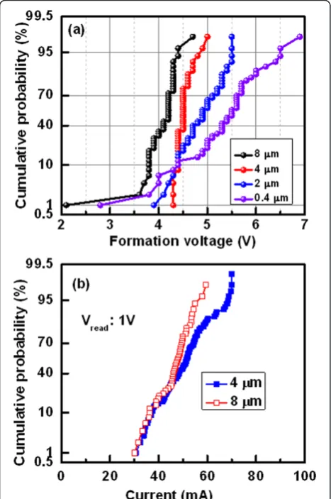
suggests that the Joule heating burns the small size de-vices at a high current as well as device size-dependent filament diameter. Heat dissipation of larger size de-vices is higher than the smaller size dede-vices. Thermal conductivities of Cu, Al, Al2O3, SiO2, TiN, and Si mate-rials are 398, 244, 25.08, 1.38, 28.84, and 148 W/m/K, re-spectively [33]. This implies that heat will be dissipated through top electrode contact than the other sides. There-fore, the area of top electrode contact as well as device size will help to reduce heating effect, especially, when the vice is operated at a high current of >10 mA. If the de-vice does not show RESET, then stronger Cu filament (or pillar) is formed into the Al2O3 layer. The forma-tion voltages (Vform) for the 8-, 4-, 2-, and 0.4-μm de-vices at 50% probability are 4.2, 4.5, 4.9, and 5.5 V, respectively (Figure 3a). Therefore, the value ofVform in-creases with decreasing the device sizes owing to lower leakage current as well as lower defects into the Al2O3
[image:4.595.57.291.319.671.2]layer. On the other hand, the formation energy is lower for larger size devices than the smaller one owing to the higher diffusion rate of Cu ions with the area. The similar phenomena of Ag diffusion in SiO2layer byin situTEM observation have been reported by Yang et al. [34]. The Cu diffusion in ZrO2 layer by TEM observation was also reported by other group [35]. The number of suc-cessful devices with different device sizes ranging from 0.4 × 0.4 to 8 × 8 μm2 is shown in Table 1. The device size of less than 2μm can carry current of 10 mA, while the larger size of 4-μm device can carry high current of 70 mA. Most important thing is that the larger size devices show 100% success, while the failure is increased with de-creasing device size. It is expected that stronger Cu pillar is needed for 3D integration of cross-point nonvolatile memory. This will be easy way and low cost for applica-tion of 3D cross-point memory [32]. Therefore, we need those devices which can sustain at high current for long time, and we find that, the devices with large area are compatible for this purpose. Figure 3b shows the statis-tical distribution of currents at low resistance state (LRS) for the device-to-devices. The mean value x and the standard deviation (σ) of currents for the 4-μm de-vices at a read voltage (Vread) of 1 V are 49.96 and 9.33 mA, while those values for the 8-μm devices are 46.14 and 6.61 mA, respectively. The read current of the 8-μm de-vices is slightly lower than that of the 4-μm devices owing to lower formation voltage. This implies that small amount of Cu diffusion into the Al2O3 films for the larger size devices than the smaller sizes. However, uniformity of the high current carrying Cu pillars is better for the 8-μm devices than those of the 4-μm de-vices. The mechanism of Cu pillar formation inside the pristine device is as follows. These are basically the CBRAM devices; however, 20-nm-thick Al2O3 film is studied for demonstration, and further study for real application of the Cu pillars into the 1-μm-thick Al2O3 films is necessary. When the positive bias is applied on the active Cu electrode, the Cuz+(z= 1,2) ion is formed by oxidation, then those ions migrate through the switch-ing medium in the presence of high electric field, and fi-nally, they become reduced at the TiN BE. This formation process transforms the pristine device from its initial
Figure 3Statistical distribution of formation voltage and current of the Cu pillars. (a)Formation voltage increases with decreasing device area which suggests the higher Cu diffusion rate for large size devices.(b)Uniform current distribution at LRS of larger device sizes implies the probability of similar conduction path of the Cu pillars.
Table 1 Device size-dependent success and failure of the Cu pillars
Device size
(μm2) Current compliance(mA) Number of successfuldevices (%)
0.4 × 0.4 10 74
1 × 1 10 78
2 × 2 10 98
4 × 4 70 100
[image:4.595.305.539.641.733.2]resistance state (IRS) to LRS as well as stronger Cu pillar is formed. By applying negative voltage on the TE, the Cu pillars of some smaller size devices are dissolved because of Joule heating. Robust Cu pillars have been investigated by measuring endurance properties below.
Figure 4 shows the read endurance characteristics with different negative read voltages. As it is bipolar device, the negative bias makes the RESET. After formation, we have increased the negative bias sequentially as −1 and−1.5 V on the TE. The current compliances are 10 and 70 mA for the 0.4- and 8-μm devices, respectively. For the 0.4-μm devices, a value of LRS is approximately 32Ω(Figure 4a), while the value is approximately 20Ω for the 8-μm devices (Figure 4b). This indicates that the
[image:5.595.56.291.271.635.2]diameter of Cu pillar is larger for the 8-μm devices than the 0.4-μm devices, as shown schematic view in the inset. For the 0.4-μm devices, the LRS state is increased after approximately 40 and 30 k cycles for the read volt-ages of −1 and −1.5 V, respectively. The Cu pillar is broken easily after higher negative voltage on the TE, as shown schematically in the inset of Figure 4a. Robust read pulse endurances of >105 cycles are obtained for the 8-μm devices because larger diameter of the Cu pil-lars, as shown schematically in the inset of Figure 4b. So, after formation of the conducting path, the possibil-ity of deterioration of the paths is less which indicates the ability of Cu pillar for 3D cross-point architecture in the future. Beside the Cu pillar investigation, the re-sistive switching characteristics of the Cu/Al2O3/TiN CBRAM devices with smaller thickness (<10 nm) of Al2O3layer are also important, which have been inves-tigated below.
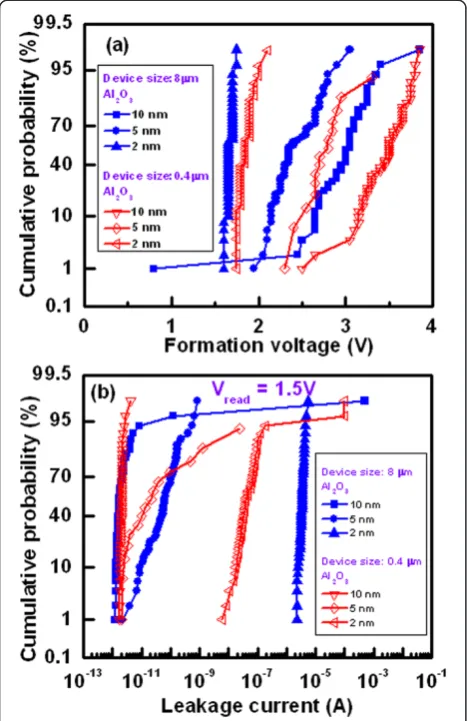
Figure 5 shows the typical I-Vcurves of the 8-μm de-vices with a 2-nm-thick Al2O3film and a CC of 500 μA is applied. The sweeping voltage is shown by arrows 1 to 5. A low Vform of 1.65 V is observed for this thin Al2O3 film. Cumulative probability of 50 CBRAM devices with different size and thickness of the Al2O3films is plotted (Figure 6a). The average values ofVformare 1.7, 2.4, and 3 V for the 8-μm devices while those values are 1.85, 2.7, and 3.4 V for the 0.4-μm devices with different thick-nesses of Al2O3 film of 2, 5, and 10 nm, respectively. Those values of Vform are lower than the 20-nm-thick Al2O3films (Figure 3a). For the 2-nm-thick Al2O3films, tight distribution of Vform is found to be 1.6 to 1.75 V and 1.75 to 2.1 V for the 8- and 0.4-μm devices, re-spectively. Figure 6b shows cumulative probability of the leakage currents for the 8- and 0.4-μm devices with
Figure 4Read pulse endurance characteristics. (a)Read pulse endurance properties degraded at high negative voltage due to the Joule heating phenomena for the smallest size devices. The Cu pillar is broken during read endurance test, which is shown in schematic view.(b)For the large size devices, long endurance reveals the robustness of the Cu pillars inside the switching medium at aVreadof−1.5 V. Long
read endurance of 105cycles is obtained for the 8-μm devices. A stronger
Cu pillar is formed into the Al2O3films, which is shown in schematic view
[image:5.595.305.538.512.694.2]inside of figure.
Figure 5I-Vswitching characteristics.Typical current-voltage characteristics of the 8-μm devices with a 2-nm-thick Al2O3film at a
thicknesses of the Al2O3films of 2, 5, and 10 nm. The leak-age currents at 50% probability are found to be 3.4μA, 60 pA, and 1.7 pA for the 8-μm devices while those values are found to be 39 nA, 22 pA, and 2.1 pA for the 0.4-μm devices with thicknesses of the Al2O3films of 2, 5, and 10 nm, respectively. The 10-nm-thick Al2O3films show device size-independent leakage currents, which is due to the limit of current measurement by our probe sta-tion. It is found that the variation of formation voltage is directly proportional to the switching material thickness and inversely proportional to the device size area. On the other hand, the leakage current shows the opposite nature of the formation voltage. It varies directly proportional to the device size and inversely proportional to the switching materials' thickness. It happens because the reduction in device size causes the decrement of defects inside the switching material which in turns increases its insulation
property. This causes the leakage current lower, and so, the required voltage to change its resistance state is more. The reduction in switching material thickness causes the higher possibility of electron tunneling through the insulator layer which causes the enhancement in leak-age current. It is observed that the 2-nm-thick Al2O3 films show better uniformity of the formation voltages as well as the leakage currents. Both the RESET current (IRESET) and voltage (VRESET) at first cycle are found to be approximately 2 mA and−0.45 V, respectively (Figure 5). The SET voltages VSET,VRESET, and IRESETat the second cycle are lower 0.5 V,−0.3 V, and approximately 540μA than those of the values that are observed in the first cycle, respectively. TheIRESETis slightly higher than the current compliance because of thinner (2 nm) Al2O3film. To dis-solve more length of the Cu filaments or to increase high resistance state (HRS), higher negative voltage of−0.8 V is required. I-Vcurves imply that the RESET is happened through a slow deterioration process of the existing metal-lic filaments in its weak point by reduction due to the negative bias on the TE. A resistance ratio (HRS/LRS) at a Vreadof 0.1 V is found to be 16, which is acceptable for application.
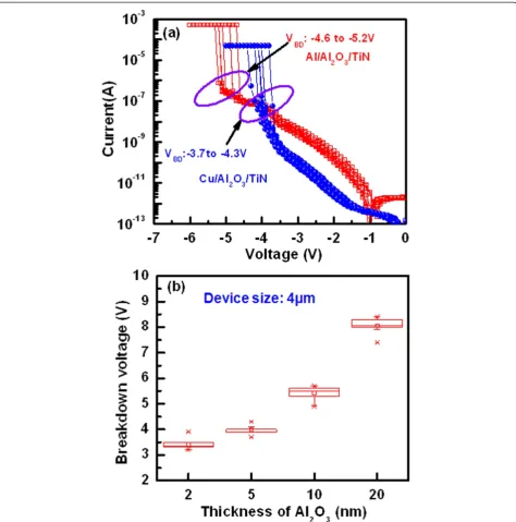
[image:6.595.57.291.90.451.2]As we have mentioned, the switching mechanism is based on Cu filament formation/dissolution into the Al2O3 film under external bias, and this could be also understood indirectly by studying the breakdown phenomenon using two different top electrodes viz. Cu and Al, as shown in Figure 7. The thickness of the Al2O3 films is 5 nm. The average breakdown voltage (VBD) of the randomly mea-sured ten devices of the Al/Al2O3/TiN structures is−4.99 V (i.e., −4.6 to −5.2 V) whereas this value of the Al/Cu/ Al2O3/TiN structures is 3.99 V (i.e., −3.7 to −4.3 V), as shown in Figure 7a. The value ofVBDis higher for the Al TE because the Al makes an additional oxide layer at the Al/Al2O3interface. According to our previous report [36], the AlOxlayer was formed at the Al/TaOx interface. It is
also found that the value ofVBDfor the Al/Cu/Al2O3/TiN structures increases with increasing the thickness of Al2O3 layer, as shown in Figure 7b. If one can compare between the breakdown voltage and the formation voltage of the Al/Cu/Al2O3/TiN structures with a 2-nm-thick Al2O3 layer, then the average value of breakdown voltage is higher than the formation voltage (−3.2 vs. 1.85 V). The similar trend is observed for all thicknesses of the Al2O3films, as discussed above. This result reveals that the formation takes place due to the Cu ion migration through the Al2O3layer. Under high electric field approxi-mately 107V/cm before breaking the stable Al-O bonds, electrochemically active Cu ions diffuse easily through the Al2O3layer and make a metallic path under a low positive voltage applied on the TE. The Cu ion migration as well as filament formation into different switching layers under external bias was also reported by other groups [16-18,24]. Figure 6Cumulative probability of formation voltage and leakage
current. (a)Formation voltages and(b)leakage currents depend on the device sizes and thickness of the Al2O3films for the Al/Cu/Al2O3/TiN
However, the switching uniformity is important of these CBRAM devices, which have been explained below.
Figure 8 shows cumulative probability of device-to-devices. The HRS and LRS for the 8- and 0.4-μm devices with a 2-nm-thick Al2O3 film are plotted. The average values ofx=σ at HRS and LRS are 5.34/4.44 kΩand 895/ 407 Ω for the 8-μm devices, respectively, while those values are 10.3/12.9 kΩand 1.07/539 kΩ for the 0.4-μm devices, respectively. The value of LRS is slightly lower for
[image:7.595.62.537.88.568.2]the 8-μm devices than the 0.4-μm devices, which is owing to higher diffusion rate of Cu ion into the Al2O3 film under external bias. By considering the resistance ratio of >2, the 0.4-μm devices show higher switching yield than that of the 8-μm devices (88% vs. 74%). This sug-gests that the 0.4-μm devices have good switching uni-formity. Figure 9 shows the statistical distribution of resistance states with different current compliances of 100, 500, and 1,000μA for the 2- and 10-nm-thick Al2O3 Figure 7Thickness-dependent Al2O3film breakdown phenomena with Cu and Al top electrodes. (a)I-Vcharacteristics show the breakdown
voltage of the Cu/Al2O3/TiN and Al/Al2O3/TiN structures. The higher breakdown voltage of Al/Al2O3/TiN than that of the Cu/Al2O3/TiN structure is
owing to oxidized Al at the Al/Al2O3interface during deposition by thermal evaporator.(b)The breakdown voltage of the Al/Cu/Al2O3/TiN structures
films. Except few devices or without proper sweeping voltage/current, there is no memory window at a CC of 100 μA. However, the value of LRS decreases and HRS remains almost the same with increasing the CCs (Figure 9a,b). The resistance ratio increases with in-creasing the CCs. Table 2 represents the average values of LRS, HRS, and HRS/LRS for the 8- and 0.4-μm de-vices with different thicknesses of Al2O3 film of 2, 5, and 10 nm. To obtain the average values, 50 CBRAM de-vices were measured. It is obvious that the resistance ratio is higher at CC of 1 mA as compared to the value at a CC of 500μA because of lower LRS value. At a CC of 500μA, a high resistance ratio of 9.6 is obtained for the 0.4-μm devices with a 2-nm-thick Al2O3film. In this case, more switchable devices are obtained (Figure 8), which is due to better control of Cu migration under external bias. The values of LRS are decreased with increasing both the device size and thickness of the Al2O3films at a CC of 500μA (Table 2), which can be explained byIRESETlater. Figure 10 shows cumulative probability of the RESET cur-rents for the 8- and 0.4-μm devices with thicknesses of the Al2O3films of 2, 5, and 10 nm at a CC of 500 μA. The averageIRESETvalues of the 2-, 5-, and 10-nm-thick Al2O3 films are found to be 706.1, 749.4, and 1,690μA, respect-ively, for the 8-μm devices, while those values are found to be 327.5, 505.4, and 1,020μA, respectively, for the 0.4-μm devices. It is observed that theIRESETvalue decreases with decreasing the thickness of the Al2O3films. Considering the thickness-dependent formation voltage (Figure 6a), the Cu ion can migrate more in the thicker Al2O3 films, resulting larger diameter of Cu filament. That is why the thicker Al2O3 film has higher RESET current. A lowest average RESET current of 327.5μA with good uniformity is obtained for the 0.4-μm devices with a 2-nm-thick
[image:8.595.307.539.89.447.2]Al2O3film (Figure 10). As mentioned above, the forma-tion voltage of the thinner Al2O3films is lower than that of the thicker one. Under SET, small amount of Cu will be migrated for the thinner Al2O3 films as well as thinner diameter of the Cu filaments. That is why the LRS value of the thinner Al2O3 films is larger than the thicker one. Under RESET, the total length of the Cu filaments will be dissolved for the thinner Al2O3 films because of both higher electric field and thinner filament diameter than that of the thicker one. On the other hand, interface-type switching or even no RESET is observed for the thicker Al2O3 films. Therefore, HRS value of the thinner Al2O3 films is higher than those of the thicker one. It can be concluded that thicker Al2O3 film can be used for the Cu pillars to apply in 3D cross-point memory and thinner one can be used for the nonvolatile resistive switching memory, and data retention test is shown below.
Figure 8Cumulative probability of HRS and LRS.The smaller size device shows superior uniformity than that of the larger size devices. It is observed that the 0.4-μm devices show 88% success for switching. The data read on the second switching cycle.
Figure 9Statistical distribution of HRS and LRS.The thicknesses of Al2O3film are(a)2 nm and(b)10 nm. The LRS decreases with
increasing the CCs of 100 to 1,000μA for the 0.4-μm devices. The 2-nm-thick Al2O3film shows superior resistance ratio than that of
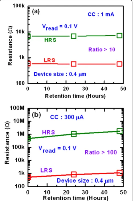
[image:8.595.58.292.89.267.2]Figure 11 shows data retention characteristics for the 0.4-μm devices with a 2-nm-thick Al2O3film. It is found the stable retention characteristics of >48 h at a CC of 1 mA (Figure 11a). The LRS is increased (slightly) with re-tention time, however, long time rere-tention of 48 h at a CC of 300μA is obtained (Figure 11b), which may be the higher dissolution rate of the existing filament at lower CC. The resistance ratio for a CC of 300μA is higher than the ratio at CC of 1 mA (100 vs. 10). At a lower CC, the small amount of the Cu atoms is responsible for the con-ducting filament formation. If small amount of Cu atoms from the thinner filament may be dissolved by neighbor defects into the AlOx film or dissolved by reading data,
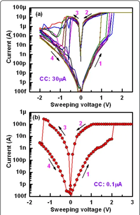
then both HRS and LRS could be increased with time. For larger diameter of the Cu filaments under higher CC, it shows stable with time because dissolution of small amount Cu from the filaments does not affect the fila-ment resistance of LRS, or even HRS. However, further study is needed to form a stronger Cu filament with thinner diameter. By adjusting measurement parameters, this CBRAM device shows forming-freeI-Vcharacteristics
[image:9.595.58.539.100.226.2]under a low CC of 30μA and a RESET current of <30μA with a high resistance ratio of >105 at a read voltage of +0.2 V (Figure 12a). This device is operated even at a lowest CC of 0.1μA (Figure 12b) with a large resistance ratio of >104, which is very useful for future nanoscale nonvolatile memory applications.
Table 2 Device size- and thickness-dependent LRS, HRS, and resistance ratio with different current compliances
Thickness of Al2O3(nm)
Device size
(μm2) Average value (Ω) and resistance ratio of HRS/LRS
CC: 500μA CC: 1 mA
LRS HRS (k) HRS/LRS LRS HRS (k) HRS/LRS
2 0.4 × 0.4 1070 10.3 9.63 502 9.8 19.55
8 × 8 895 5.34 5.97 384 22.3 58.10
5 0.4 × 0.4 826 4.64 5.62 487 3.6 7.39
8 × 8 652 4.54 6.96 364 18.3 50.27
10 0.4 × 0.4 572 1.71 3.00 394 2.48 6.3
[image:9.595.306.540.340.694.2]8 × 8 492 1.48 3.00 343 2.05 6.0
Figure 10RESET current distribution.The RESET currents depend on the thickness of the Al2O3films and device sizes. The 0.4-μm devices
with a 2-nm-thick Al2O3film show the lowest RESET current distribution
as compared to the others at a CC of 500μA.
[image:9.595.57.292.505.684.2]Conclusions
The device size- and thickness-dependent Cu pillars and resistive switching memory characteristics using the Al/ Cu/Al2O3/TiN CBRAM devices have been investigated. The stronger Cu pillars with yield of 100% are formed into the Al2O3films for the larger size devices at a high CC of 70 mA, which is due to the easy heat dissipation effect. Robust Cu pillar with a long endurance of >105 cycles is obtained even a high negative voltage of−1.5 V, which promises for future 3D cross-point memory appli-cations. Improved resistive switching memory character-istics such as high switching yield of 88%, low voltage operation of ±2 V, and lower average RESET current of 327.5μA for a CC of 500μA are obtained for the 0.4-μm devices with a 2-nm-thick Al2O3 film. The formation/ dissolution of the Cu filaments into a 2-nm-thick Al2O3 film is responsible to have better switching characteristics under external bias because of thinner film. On the other
hand, Cu diffusion rate is higher for the larger size and thicker film which will have inferior switching charac-teristics, however, give us superior Cu pillars. Good data retention characteristics of 48 h are obtained at a CC of 300μA. This device shows forming-freeI-Vcharacteristics under a lowest CC of 0.1 μA with a high resistance ratio of >104. This strategy on the Cu pillars and resistive switching memory characteristics of the Cu/Al2O3/TiN CBRAM devices will help to develop in future 3D cross-point architecture with low cost applications.
Competing interests
The authors declare that they have no competing interests.
Authors’contributions
RP fabricated the CBRAM devices under the instruction of SM. DJ helped also partially to fabricate the devices. RP measured all the devices under the instruction of SM. SR and DJ measured also the CBRAM devices partially under the instruction of SM. All authors contributed to the revision of the manuscript, and they approved it for publication.
Acknowledgements
This work was supported by National Science Council (NSC) Taiwan, under contract no. NSC-102-2221-E-182-057-MY2. The authors are also grateful to Electronics and Optoelectronics Research Laboratories (EOL)/Industrial Technology Research Institute (ITRI) in Hsinchu, Taiwan for their experimental support.
Received: 29 November 2014 Accepted: 8 December 2014 Published: 23 December 2014
References
1. Prakash A, Jana D, Maikap S:TaOxbased resistive switching memories:
prospective and challenges.Nanoscale Res Lett2013,8:418.
2. Yang JJ, Strukov DB, Stewart DR:Memristive devices for computing.Nat Nanotechnology2013,8:13.
3. Torrezan AC, Strachan JP, Medeiros-Ribeiro G, Williams RS:Sub-nanosecond switching of a tantalum oxide memristor.Nanotechnology2011,22:485203. 4. Lee HY, Chen PS, Wu TY, Chen YS, Wang CC, Tzeng PJ, Lin CH, Chen F,
Lien CH, Tsai MJ:Low power and high speed bipolar switching with a thin reactive Ti buffer layer in robust HfO2based RRAM.Tech Dig - Int Electron Devices Meet. San Francisco, CA; 2008:1–4.
5. Chen YS, Lee HY, Chen PS, Liu WH, Wang SM, Gu PY, Hsu YY, Tsai CH, Chen WS, Chen F, Tsai MJ, Lien C:Robust high-resistance state and improved endurance of HfOxresistive memory by suppression of current overshoot.IEEE Electron Device Lett2011,32:1585.
6. Wu Y, Yu S, Lee B, Wong HSP:Low-power TiN/Al2O3/Pt resistive switching
device with sub-20μA switching current and gradual resistance modulation.J Appl Phys2011,110:094104.
7. Lin CY, Wu CY, Hu C, Tseng TY:Bistable resistive switching in Al2O3
memory thin films.J Electrochem Socvol2007,154:G189.
8. Banerjee W, Maikap S, Rahaman SZ, Prakash A, Tien TC, Li WC, Yang JR: Improved resistive switching memory characteristics using core-shell IrOx
nano-dots in Al2O3/WOxbilayer structure.J Electrochem Soc2012,
159:H177.
9. Prakash A, Maikap S, Banerjee W, Jana D, Lai CS:Impact of electrically formed interfacial layer and improved memory characteristics of IrOx/
high-κx/W structures containing AlOx, GdOx, HfOx, and TaOxswitching
materials.Nanoscale Res Lett2013,8:379.
10. Afanas’ev VV, Stesmans A:Internal photoemission at interfaces of high-k insulators with semiconductors and metals.J Appl Phys2007,102:08130. 11. Yu HY, Li MF, Cho BJ, Yeo CC, Joo MS, Kwong DL, Pan JS, Ang CH, Zheng JZ, Ramanathan S:Enery gap and band alignment for (HfO2)x(Al2O3)1-xon (100)
Si.Appl Phys Lett2002,81:376.
12. Robertson J:High dielectric constant oxides.Eur Phys J Appl Phys2004, 28:265.
[image:10.595.56.291.89.448.2]13. Dean JA:Lange’s Handbook of Chemistry.896.
Figure 12I-Vcurves a low CC of 30μA.TypicalI-Vcharacteristics under a CC of(a)30μA with a thickness of the Al2O3layer of 5 nm
and(b)at a lowest CC of 0.1μA. Forming-freeI-Vcharacteristics are observed. A high resistance ratio of >104at a read voltage of 0.2 V is
14. Wu Y, Lee B, Philip Wong HSP:Ultra-low power Al2O3-based RRAM with 1
μA reset current.InInternational Symposium on VLSI Technology Systems and Applications (VLSI-TSA).Hsinchu; 2010:136–137.
15. Kund M, Beitel G, Pinnow CU, Röhr T, Schumann J, Symanczyk R, Ufert KD, Müller G:Conductive bridging RAM (CBRAM): An emerging non-volatile memory technology scalable to sub 20 nm.InTech Dig - Int Electron Devices Meet. (IEDM).Washington, DC: 2005:754–757.
16. Rahaman SZ, Maikap S, Das A, Prakash A, Wu YH, Lai CS, Tien TC, Chen WS, Lee HY, Chen FT, Tsai MJ, Chang LB:Enhanced nanoscale resistive switching memory characteristics and switching mechanism using high-Ge-content Ge0.5Se0.5solid electrolyte.Nanoscale Research Lett2012,7:614.
17. Valov I, Waser R, Jameson JR, Kozicki MN:Electrochemical metallization memories-fundamentals, applications, prospects.Nanotechnology2011, 22:254003.
18. Jameson JR, Gilbert N, Koushan F, Saenz J, Wang J, Hollmer S, Kozicki M, Derhacobian N:Quantized conductance in Ag/GeS2/W conductive-bridge
memory cells.IEEE Electron Device Lett2012,33:257.
19. Kwak JS, Chi EJ, Choi JD, Park SW, Baik HK, So MG, Lee SM:Prediction of solid‐state amorphizing reaction using effective driving force.J Appl Phys 1995,78:983.
20. Banno N, Sakamoto T, Iguchi N, Sunamura H, Terabe K, Hasegawa T, Aono M: Diffusivity of Cu ions in solid electrolyte and its effect on the performance of nanometer-scale switch.IEEE Trans Electron Devices2008,55:3283. 21. Kaeriyama S, Sakamoto T, Sunamura H, Mizuno M, Kawaura H, Hasegawa T,
Terabe K, Nakayama T, Aono M:A nonvolatile programmable solid-electrolyte nanometer switch.IEEE J Solid-State Circuits2005,40:168. 22. Xu Z, Bando Y, Wang W, Bai X, Golberg D:Real-timein-situHRTEM-resolved
resistance switching of Ag2S nanoscale ionic conductor.ACS Nano2010,
4:2515.
23. Terabe K, Hasegawa T, Nakayama T, Aono M:Quantized conductance atomic switch.Nature2005,433:47.
24. Goux L, Opsomer K, Degraeve R, Müller R, Detavernier C, Wouters DJ, Jurczak M, Altimime L, Kittl JA:Influence of the Cu-Te composition and microstructure on the resistive switching of Cu-Te/Al2O3/Si cells.Appl Phys Lett2011,99:053502.
25. Sleiman A, Sayers PW, Mabrook MF:Mechanism of resistive switching in Cu/AlOx/W nonvolatile memory structures.J ApplPhys2013,113:164506.
26. Belmonte A, Kim W, Chan BT, Heylen N, Fantini A, Houssa M, Jurczak M, Goux L:90 nm W\Al2O3\TiW\Cu 1T1R CBRAM cell showing low-power,
fast and disturb-free operation.International Memory Workshop (IMW)2013. 27. Tanaka H, Kido M, Yahashi K, Oomura M, Katsumata R, Kito M, Fukuzumi Y,
Sato M, Nagata Y, Matsuoka Y:Bit cost scalable technology with punch and plug process for ultra high density flash memory.Kyoto: Tech Dig Symp VLSI Technol; 2007:14–15.
28. Kim W, Choi S, Sung J, Lee T, Park C, Ko H, Jung J, Yoo I, Park Y:Multi-layered vertical gate NAND flash overcoming stacking limit for terabit density storage. Honolulu, HI: Tech Dig Symp VLSI Technol; 2009:188–189.
29. Jang J, Kim HS, Cho W, Cho H, Kim J, Shim S, Jang Y, Jeong J, Son BK, Kim DW, Kim K, Shim JJ, Lim JS, Kim KH, Yi SY, Lim JY, Chung D, Moon HC, Hwang S, Lee JW, Son YH, Chung UI, Lee WS:Vertical cell array using TCAT (Terabit Cell Array Transistor) technology for ultra high density NAND flash memory.Honolulu, HI: Tech Dig Symp VLSI Technol; 2009:192–193.
30. Katsumata R, Kito M, Fukuzumi Y, Kido M, Tanaka H, Komori Y, Ishiduki M, Matsunami J, Fujiwara T, Nagata Y, Zhang L, Iwata Y, Kirisawa R, Aochi H, Nitayama A:Pipe-shaped BiCS flash memory with 16 stacked layers and multi-level-cell operation for ultra high density storage devices.Honolulu, HI: Tech Dig Symp VLSI Technol; 2009:136–137.
31. Joblot S, Bar P, Sibuet H, Ferrandon C, Reig B, Jan S, Arnaud C, Lamy Y, Coudrain P, Coffy R, Boillon O, Carpentier JF:Copper pillar interconnect capability for mm wave applications in 3D integration technology. Microelectron Eng2013,107:72.
32. Maikap S, Panja R, Jana D:Copper pillar and memory characteristics using Al2O3switching material for 3D architecture.Nanoscale Res Lett2014,
9:366.
33. A MEMS clearinghouse and information portal for the MEMS and nanotechnology community.http://www.memsnet.org/news/ and http:// en.wikipedia.org/wiki/Silicon.
34. Yang Y, Gao P, Gaba S, Chang T, Pan X, Lu W:Observation of conducting filament growth in nanoscale resistive memories.Nature Comm2012,3:1.
35. Liu Q, Sun J, Lv H, Long S, Yin K, Wan N, Li Y, Sun L, Liu M:Real-Time observation on dynamic growth/dissolution of conductive filaments in oxide-electrolyte-based ReRAM.Adv Mater2012,24:1844.
36. Prakash A, Maikap S, Chen WS, Lee HY, Chen F, Tien TC, Lai CS:Device size-dependent improved resistive switching memory performance. IEEE Trans Nanotech2014,13:409.
doi:10.1186/1556-276X-9-692
Cite this article as:Panjaet al.:Impact of device size and thickness of Al2O3film on the Cu pillar and resistive switching characteristics for 3D cross-point memory application.Nanoscale Research Letters20149:692.
Submit your manuscript to a
journal and benefi t from:
7 Convenient online submission
7 Rigorous peer review
7 Immediate publication on acceptance
7 Open access: articles freely available online
7 High visibility within the fi eld
7 Retaining the copyright to your article