Liquid Interfaces and Metal/Nanogap Junctions
Thesis
by
Florian
Gstrein
In Partial Fulfillment of the Requirements
For the Degree of Doctor of Philosophy
California Institute of Technology
Pasadena, California
2004
This thesis is dedicated to my uncle
Hofrat
Dr. H. Peter Wagner
Meteorologist
A wise and slightly cynical postdoctoral scholar in the Lewis group once told me
as he was pacing up and down the noble hallways of Noyes, “The only thing people are
really interested in when reading your thesis are the acknowledgements. So acknowledge
everyone and everything!” If this statement is correct, I had better do justice to the
expectations of my readership! I have done my best in compiling the following list of
people who all have made important contributions to my Ph.D. thesis and I apologize for
any omissions.
It gives me great pleasure to thank my advisor, Prof. Nathan S. Lewis, for his
outstanding mentorship and friendship. Nate is an exceptional advisor, inspiring scientist
and without a shadow of a doubt the smartest man I have ever met. The most important
thing I have learned from Nate is that experimental science can only be done by
approaching a scientific question thoroughly and carefully from various angles and by
carrying out the appropriate control experiments.
Dr. Helfried Näfe (Max Planck Institute for Metals Research, Stuttgart, FRG) and
Dr. Dimitrij I. Bronin (Institute of High-Temperature Electrochemistry, Russian Academy
of Sciences, Ural Branch, Ekaterinburg, Russian Federation) were the most influential
mentors in my pre-Caltech days. Their shining example and integrity as researchers left
me with no other choice but to pursue academic research.
I would like to thank my co-advisors, Prof. Michael Roukes and Prof. James C.
Hone, who is now at Columbia University. Michael not only allowed me to work in his
magnificent laboratory in the Department of Physics, but he also fully integrated me into
his research group. Not many outsiders belong to the inner circle of the Roukes group, and
I am grateful for Michael’s genuine and continued interest in my research project. Jim, the
I am looking forward to our collaboration on various levels in the future. I also learned
from Jim that you can buy an entire lab on eBay, but that you cannot “buy” a car from him.
There are many members of the Lewis and Roukes group who have worked with
me closely on several projects. Tom Hamann did an outstanding job in synthesizing many
of the osmium compounds for the ZnO project and in studying their self-exchange
properties. Dr. William Royea and David Michalak worked with me closely on studies of
the surface recombination behavior of silicon. In particular, Dave carried out most of the
rf-conductivity measurements. I would like to thank Prof. Adrian Lew (Stanford
University) and Dr. Reiner Nürnberg (Weierstrass Institute, Berlin) for many useful
discussions regarding the TeSCA simulations. The NIRT project was a collaborative effort
of many people. Jim’s leading role has already been mentioned. My friend Dr. Srivatsan
Nagarajan came up with many original ideas regarding this project and contributed in
setting up the early instrumentation. Working with Leon Bellan, who did his senior thesis
work with me, was the most pleasant experience I had at Caltech. Leon contributed greatly
in setting up the measurement system in its present form. I would also like to thank Ali
Hussain (Scherer group), Carol Garland (TEM work) and Drs. Hongxin Tang, Darron
Young, Hidehiro Yoshida, and Henk Postma (all Roukes group) for their helping hands
with many NIRT experiments.
I am also indebted to many Lewis group members present and past for good
discussions and their support, especially, Dr. Shawn “Sean” Briglin, Lauren “Lorraine”
Webb, Jordan Katz, Prof. George Coia (the wise old postdoc), Prof. Sami Anz, Dr. Will
Royea, Dr. Rob Rossi, Dr. Glen Walker, Prof. Mike Freund, Dr. Bruce Brunschwig, Dr.
Jae-Joon Lee, Dr. Arnel Fajardo and two exceptional administrative assistants of Nate’s,
Nannette Pettis and Sherry Feick. Among all Lewis groupies, Mr. David J. Michalak
thesis would have made much sense and Prof. Bill Goddard for two exceptionally well-
taught classes, which convinced me that I better stay far away from computational
chemistry. Many of the experiments would have been impossible without Mike Roy and
Guy Duremberg (Instrument Shop), Tom Dunn (Electrical Shop), and the great Nils
Apslund (Roukes Group).
Last but certainly not least I would like to thank the many outstanding people that I
met during graduate school for their friendship, love and spiritual support. In no particular
order these individuals are Adri Lew and Patri Strass (now at Stanford), Alex Bäcker, Eva
Peral, Veronica & Pablito (all Pasadena), Julian Chaubell & Nance (Pasadena), Mathias
Libedinsky (now in Jerusalem), Ronen Almog (now at the Technion in Haifa), Mathias
Zielonka, Alejandra Engelberg, and Sebastian (all Pasadena), Eva Rüba (now in Vienna),
Christoph Sonnlechner (now in Vienna), Ines Schwetz (now in Graz), and my dear
landlords and friends Robert and Carolyn Volk (San Marino).
Finally, I would like to thank my family back in Austria, first and foremost my
parents, Hans-Jürgen & Edith Gstrein, and my sister, Marlis, for their relentless moral
Abstract
This thesis presents recent progress made in the understanding of charge-transfer
kinetics and charge-carrier dynamics at semiconductor/liquid interfaces and presents a
study of the charge-transport characteristics of nanostructured electrodes for the study of
electron tunneling through molecules.
It is shown that n-ZnO/H2O-A/A- junctions (where A/A- corresponds to
[Fe(CN)6]3-/4-, [Co(bpy)3]3+/2+, or [OsL2L’]3+/2+) display energetic and kinetic behavior of unprecedented ideality for the experimental determination of robust rate constants for
electron transfer from n-type semiconductors to electron acceptors in solution. The
reorganization energies of these redox couples were for the first time determined
independently through NMR line-broadening experiments. Semiconductor/liquid contacts
with an electrochemical driving force larger than the driving force at the point of optimum
exoergicity showed lower rate constants than contacts with a lower driving force. The rate
constant for charge transfer of the junction with the highest driving force increased when
the driving force was lowered. This was done by decreasing the pH of the contacting
electrolyte, which shifted the conduction-band edge of the OH-terminated n-ZnO to more
positive values. This indicates that the contact with the largest driving force operated in
the inverted regime of charge transfer. The rate constant of the contact with the lowest
driving force (∆Go’ << 0.7 eV), on the other hand, decreased when the conduction-band edge was shifted to more positive values, which indicates that the low-driving force
contact operated in the normal regime of charge transfer. These results provide for the first
time a direct and credible experimental indication that semiconductor/liquid contacts can
indeed operate in the inverted regime. Semiconductor/liquid contacts, which had a similar
driving force but different reorganization energies showed the expected dependence of the
interfacial energetics. Low effective surface recombination velocities (SRVs)were
observed for systems capable of undergoing interfacial charge-transfer reactions that
produce an accumulation of holes or an accumulation of electrons at the Si surface. In
conjunction with near-surface channel conductance measurements, it was revealed that the
formation of an accumulation of holes or the formation of an accumulation of electrons
and not a reduced density of electrical trap sites on the surface, is primarily responsible for
the long charge-carrier lifetimes observed for Si surfaces. Digital simulations
incorporating a generalized Shockley-Read-Hall model for surface recombination
revealed that effective surface recombination velocities < 10 cm s-1 can be produced by surfaces having a density of electrical traps as large as 1012 cm-2 provided that the surface is in accumulation or inversion due to charge-transfer equilibration with the redox-active
electrolyte. Silicon in contact with aqueous fluoride solutions exhibit low SRVs. Some
reports in the past have suggested that the defect density of Si in acidic solutions is
reduced by the protonation of defect sites. Alternatively, this study shows that an
accumulation of electrons at the surface can lead to low SRVs. The degree of band bending
and SRVs of Si(111) in contact with a variety of aqueous fluoride solutions were
determined for the first time at open circuit conditions. The accumulation of electrons at
the surface is responsible for the low effective SRVs in NH4F and buffered HF solutions. The reversible protonation of basic defect sites might be important for the low SRV of
n-Si(111)/H2SO4(aq) contacts but plays a minor role in the recombination behavior of Si in contact with aqueous fluoride solutions.
Electromigration-induced breaking of metal nanowires is a promising new method
that has recently been employed in the formation of metal-molecule-metal tunnel
studied. In this work, the current vs. voltage (J vs. E) characteristics of electron-tunnel
junctions formed by the electromigration of metal nanowires without a molecule bridging
the gap were explored in detail. Junctions displayed J vs. E characteristics with a variety of
shapes and current magnitudes. The low-temperature J vs. E curves of some junctions
showed regions of zero conductivity near zero bias. Such features were absent in the data
collected for other tunnel junctions. These differences notwithstanding, a common pattern
was discerned in that the low-bias resistances of the vast majority of the junctions
decreased by an order of magnitude or more with increasing temperature. The features
detected in this study are consistent with the Coulomb blockade effect. We attribute the
blockade behavior to metal atom clusters or islands located in the nano-sized gap region.
This assignment is compatible with the mechanism of electromigration. In support of this
interpretation, it was found that the low-bias resistance vs. temperature curves were well
described by Abeles' model for electron tunneling in granular metal junctions. Additional
support for the assignment was obtained from TEM studies of gold junctions with
chromium adhesion layers, where the images showed the presence of a thin granular film
Table of Contents
Acknowledgments . . . iv
Table of Contents . . . xi
List of Figures . . . xiii
List of Tables . . . xv
Chapter 1. Introduction to Electron-Transfer Processes at Semiconductor/Liquid Interfaces and Metal/Nanogap Junctions
1.1 Overview . . . 1-2 1.2 Energetics of the Semiconductor/Liquid Interface . . . 1-3 1.3 Comparison between Semiconductor and Metal Electrodes . . . 1-12 1.4 References . . . 1-13
Chapter 2. Energetics of Electron-Transfer Reactions at the n-type ZnO(0001)/ Liquid Interface
2.1 Introduction . . . 2-2 2.2 Background . . . 2-4 2.3 Experimental . . . 2-10
2.3.1 Electrode Preparation . . . 2-10 2.3.2 Electrochemical Measurements . . . 2-13 2.3.3 Redox Compounds and Solutions . . . 2-18
2.4 Results . . . 2-26
2.4.1 Results of Cdiff -E Measurements . . . 2-27
2.4.2 Results of J-E Measurements . . . 2-45 2.4.3 Determination of Electron-Transfer Rate Constants (ket) . . . 2-54 2.4.4 Trends in the ket Values for n-Zn(0001)/Liquid Contacts. . . . 2-58 2.4.5 Rate Constants of n-ZnO in Contact with [Fe(CN)6]3-/4-, [Co(bpy)3]3+/2+, or [Ru(NH3)5py]3+/2+ . . . 2-64
2.5 Discussion . . . 2-67
2.5.1 Energetic Behavior of n-ZnO(0001)/Liquid Contacts . . . 2-67 2.5.2 Kinetic Behavior of n-Zn(0001)/Liquid Contacts . . . 2-73
2.6 Conclusions . . . 2-79 2.7 References . . . 2-81
Chapter 3. Effects of Interfacial Energetics on the Charge Carrier Dynamics at Silicon/Liquid Contacts
3.2 Background . . . 3-5 3.3 Experimental . . . 3-10
3.3.1 Digital Simulations . . . 3-10 3.3.2 Photoconductivity Decay Measurements . . . 3-13 3.3.3 Measurement of the Built-in Voltage of Si/H2O Contacts Using Differential Capacitance Measure-ments . . . 3-15 3.3.4 Measurement of the Built-In Voltage of Si/Liquid Contacts Using a Near-Surface Channel Conduc-tance Method . . . 3-19 3.3.5 Materials & Chemicals . . . 3-24
3.4 Results . . . 3-26
3.4.1 Digital Simulation of Photoconductivity Decay Dynamics for Si/Liquid Contacts . . . 3-26 3.4.2 Photoconductivity Decay Measurements of Hydrogen-Terminated Si(111) . . . 3-38 3.4.3 Measurement of the Built-In Voltage of n-Si(111)/H2O Contacts Using Differential Capacitance Measurements . . . 3-44 3.4.4 Near-Surface Channel Conductance Measurements . . . 3-55
3.5 Discussion . . . 3-77
3.5.1 The Influence of Interfacial Energetics on the Surface Recombination Velocity of Inverted n-Si(111) Contacts . . . 3-77 3.5.2 Comparison between Digital Simulations and Experimental Observations of the Surface Recombi-nation Velocity as a Function of the Redox Potential of the Electrolyte . . . 3-81 3.5.3 The Influence of Interfacial Energetics on the Surface Recombination Velocity of n-Si(111)/ CH3CN Contacts and n-Si(111)/H2O Contacts . . . 3-83
3.6 Conclusions . . . 3-88 3.7 References . . . 3-89
Chapter 4. Electron-Transfer Processes at Metal/Nanogap Junctions
4.1 Introduction . . . 4-2 4.2 Background . . . 4-5 4.3 Experimental . . . 4-12
4.3.1 Device Fabrication . . . 4-13 4.3.2 Electrical Measurements . . . 4-21
List of Figures
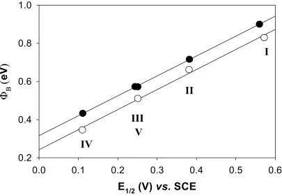
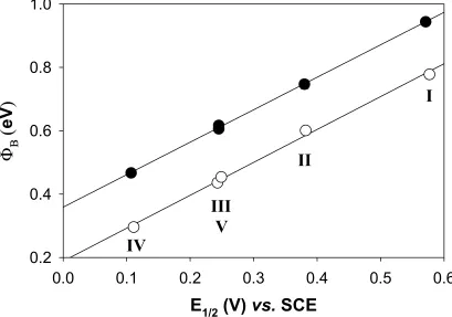
FIGURE 1.1 Band Diagrams and Charge-Carrier Profiles of n-type and p-type Semicon-ductor/Liquid Junctions. . . 1-4 FIGURE 2.1 Thermodynamic and Kinetic Parameters of a General Semiconductor/Liquid Junction in the Presence of Ionized Surface States. . . 2-6 FIGURE 2.2 Equivalent Circuit and Its Simplifications. . . 2-16 FIGURE 2.3 Chemical Structures of Redox Compounds Used in This Work. . . 2-19 FIGURE 2.4 Representative Bode Plot for a n-ZnO(0001)/H2O Junction. . . 2-28 FIGURE 2.5 Mott-Schottky Plots for Junctions ZnO1_I_pH8 to ZnO1_V_pH8.. . . 2-34 FIGURE 2.6 Plot of the Barrier Height vs. E1/2 for Various n-ZnO(0001) Semiconductor/ Liquid Contacts. . . 2-42
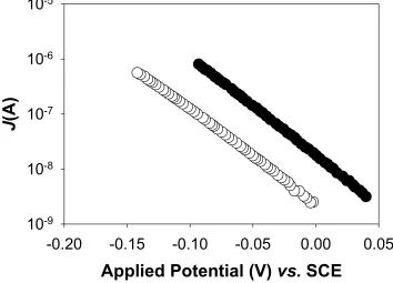
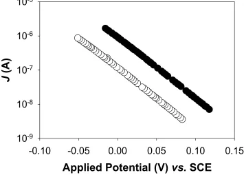
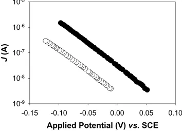
FIGURE 2.7 Dark J-Ecorr Characteristics for Junctions ZnO1_I_pH8 to ZnO1_V_pH8.
. . . 2-47 FIGURE 2.8 Plots of Electron-Transfer Rate Constants (ket) vs. Driving Force for Charge Transfer. . . 2-59 FIGURE 2.9 Influence of Trap States on Mott-Schottky Plots. . . 2-69 FIGURE 2.10 Plots of the Electron-Transfer Rate Constant as a Function of Driving Force and Reorganization Energy. . . 2-75 FIGURE 3.1 Energy Band Visualization of Recombination Processes. . . . 3-6 FIGURE 3.2 Schematic Drawing of the Fabrication of n+-p-Si(111)-n+ Devices . . . . 3-22 FIGURE 3.3 Charge-Carrier Concentration Profiles for Si/Me2Fc+/0 Contacts. . . 3-31 FIGURE 3.4 Charge-Carrier Concentration Profiles for Si/Me10Fc+/0 Contacts. . . 3-35 FIGURE 3.5 Time-Resolved Photoconductivity Decay. . . 3-39 FIGURE 3.6 Measured Lifetimes of H-terminated Si(111) Following Various Surface Treatments. . . 3-45 FIGURE 3.7 Parallel Capacitance vs. Applied Potential under Forward Bias for H-Termi-nated n-Si(111)/H2O Contacts. . . 3-52 FIGURE 3.8 Equivalent Circuits for the Transconductance Arrangement containing 3 Im-pedance Pathways. . . . 3-57
FIGURE 3.9 Impedance Spectrum of a n+-p-Si(111)-n+ Device with a 1-Micron- Thick
with 5 mM CoCp2+/0. . . 3-61 FIGURE 3.11 Representative Impedance Data for a n+-p-Si(111)-n+ Device in Contact with 5 mM Me10Fc+/0. . . 3-63 FIGURE 3.12 Representative Impedance Spectra for a n+-p-Si(111)-n+ Device in Contact with Various CH3CN Solutions.. . . 3-65 FIGURE 3.13 Representative Impedance Spectra for a n+-p-Si(111)-n+ Device in Contact with Various Aqueous Fluoride Solutions and 18 M H2SO4(aq). . . 3-71
FIGURE 3.14 Low-Frequency Intercepts of the Impedance of H-terminated n+-p-Si(111)-
n+ Near-Surface Channel Conductance Devices Following Various Surface Treatments.
. . . 3-73 FIGURE 3.15 Surface Recombination Velocities and the Corresponding Surface State Trap Densities of Various Si Surfaces. . . 3-78 FIGURE 4.1 Energy Band Diagram for Electron Transfer in Electron Tunnel Junctions and Metal Island Films. . . 4-6 FIGURE 4.2 Tunneling Current vs. Applied Potential as a Function of the Barrier Height. . . . 4-9 FIGURE 4.3 Schematic of the Experimental Setup of Electromigration Experiments. 4-14 FIGURE 4.4 Fabrication of Nanostructured Electrodes Using Shadow Evaporation.. 4-17 FIGURE 4.5 Measurement System for the Electrical Characterization of Electron Tunnel-ing Gaps as a Function of Temperature and Gate Bias. . . 4-22 FIGURE 4.6 Electrical Circuit Diagrams for Switch System, Electromigration
Experi-ments, Differential Conductance Measurements and Measurement of the J-E
Characteris-tics. . . 4-26 FIGURE 4.7 Current and Conductivity Changes during Electromigration.. . . 4-30 FIGURE 4.8 (a) J-E Characteristics of Devices of Type I. (b) Plot of Low-Bias resistance
vs. T-1/2 and Plot of Differential Resistance vs. E-1. (c) TEM Images After Electromigra-tion. . . 4-35 FIGURE 4.9 J-E Characteristics of a Device of Type II as a Function of Temperature
. . . 4-40 FIGURE 4.10 (a) J-E Characteristics of a Device of Type IV as a Function of Temperature and Gate Bias. (b) SEM Images of Electromigrated Devices. . . 4-45 FIGURE 4.11 (a) J-E Characteristics of a Device of Type IV as a Function of Temperature.
List of Tables
TABLE 2.1 Impedance data for junctions ZnO1_I_pH8-ZnO1_V_pH8 . . . 2-30
TABLE 2.2 Average values of the flat-band potential (Efb) and of the dopant density (ND) for the n-ZnO(0001)/liquid junctions. . . . 2-40
TABLE 2.3 J-E Data for n-ZnO(0001)/liquid junctions . . . 2-53
TABLE 2.4 Barrier heights (ΦB) and rate constants (ket) for n-ZnO(0001)/liquid junctions. . . . 2-55
TABLE 2.5 Results of rate constant measurements involving electrode ZnO3 and redox compounds VI, VII, VIII. . . . 2-66
TABLE 3.1 Physical input parameters of the TeSCA simulations . . . 3-16
TABLE 3.2 Simulation results. . . 3-27
TABLE 3.3 Measured lifetimes and surface recombination velocities for H-terminated Si(111) following various surface treatments. . . 3-42
TABLE 3.4 Measured lifetimes and surface recombination velocities for NH4F(aq)-etched n-Si(111) following various surface treatments in aqueous solutions.. . . 3-48
1.1 OVERVIEW
For a long time, electrochemists have viewed the electrode simply as an electronic
conductor of low resistivity that serves as a source or sink of electrons. The influence of
charge-transfer kinetics and charge-carrier dynamics at the surface of an electrode have
only been vaguely connected to the electronic and energetic properties of individual
charge carriers in the electrode and the electronic interaction of that electrode with a redox
couple in solution. According to the late Heinz Gerischer (1919-1994), by many
considered to be the field’s most influential proponent, the modern concept of electrode
kinetics is largely due to the introduction of semiconductors as electrode materials and the
advent of electron-transfer theory.1
This thesis presents recent progress made in our understanding of charge-transfer
kinetics and charge-carrier dynamics at semiconductor/liquid interfaces and presents an
investigation of the fundamental properties of nanostructured electrodes for the study of
electron tunneling through molecular bridges and solvents. In Chapter 2 of this thesis,
ZnO (0001) single-crystal electrodes in contact with a series of non-adsorbing redox
couples in solution are presented as model systems of unprecedented ideality for the study
of the energetics of electron-transfer processes. Chapter 3 of this thesis shows that the
dynamics of charge carrier recombination at the semiconductor/liquid interface can be
consistently explained through reference to the interfacial energetics. The same concept
can also be applied to the complex but technologically relevant charge-carrier dynamics at
the surface of Si single crystals in contact with aqueous fluoride etching solutions. Chapter
4 deviates from the field of semiconductor electrochemistry somewhat and addresses
charge-transfer processes in metal nanoelectrodes separated by less than 1 nanometer.
Such experiments are important in understanding the energetics of electron tunneling
interface. The electrostatics of this junction will be developed in a mathematically
rigorous fashion using Poisson’s equation and the Gauss relation. Special concepts
regarding the kinetics of charge transfer across the semiconductor/liquid interface and the
Shockley-Read-Hall model of charge-carrier recombination will be introduced in Chapter
2 and Chapter 3, respectively. The energetics of electron tunneling will be discussed in
Chapter 4.
1.2 ENERGETICS OF THE SEMICONDUCTOR/LIQUID
INTERFACE
One of the most fundamental properties of semiconductor electrodes is that diffuse
double layers can not only exist in the form of ionic double layers, which are so familiar
from studies involving metallic electrodes, but can also exist in form of diffuse
space-charge layers inside the semiconductor electrode itself. This space-space-charge layer usually
dominates the capacitance of the electrode. Conceptually, this space-charge layer is
identical with semiconductor-metal junctions and models developed by physicists have
thus been successfully adapted for semiconductor/liquid junctions.
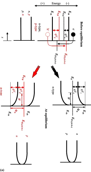
The energy band diagrams of an n-type semiconductor and a p-type semiconductor
in contact with a liquid are shown in Figure 1.1 (a) before and after equilibration of the
Fermi levels together with the charge-carrier profiles for electrons and holes. The
equilibration processes at semiconductor/liquid junctions involving either n-type or p-type
electrodes are so closely related that the description will be restricted to the case of an
n-type semiconductor. The equilibration process and the definition of parameters of a p-n-type
Figure 1.1 Band Diagrams and Charge-Carrier Profiles of n-type and p-type
Semi-conductor/Liquid Junctions.
The reference energy has been shifted from the vacuum level to an arbitrary value on the
electrochemical energy scale (for instance cell potential). (a) Before charge
equilibration, the energy bands and charge-carrier profiles are uniform and the entire
semiconductor is neutral. To achieve depletion the electrochemical potential or the
Fermi level of the solution is more positive (in the case of p-type more negative) than the
Fermi level, EF, of the semiconductor. As a result electrons (in the case of p-type: holes)
are injected from the conduction band (in the case of p-type: valence band) to acceptor
species in solution. The charge transfer will continue until the initial difference in the
Fermi levels is neutralized. After charge equilibration a depletion layer is formed in the
semiconductor, i.e., a non uniform charge distribution in the semiconductor. An excess
of positive charges (p-type: negative charges) in the depletion width W and in the
solution an excess of negative charges (p-type: positive charges) evolves. This results in
a electric potential gradient (band bending) in the semiconductor. The parameter qVn is defined as the difference between EF and Ecb, and qVs is the surface barrier of the junction. The surface barrier can be modulated by the applied potential (Eapp) and is typically expressed as Vs = Vbi + Eapp. The surface barrier of the junction in the absence of an applied potential (Vbi) is referred to as the built-in voltage. The barrier height of the junction, ΦB is defined as ΦB = qVn + qVs. Subscript “n” and “p” denote n-type or p-type semiconductor, respectively. (b) Three special equilibrium conditions for an n-p-type
semiconductor: (I) flat-band condition (no difference in Fermi levels or Fermi level of
the semiconductor is shifted accordingly by applying an external potential) (II) inversion
(very positive solution potential), and (III) accumulation (very negative solution
n p E F Be fo re e qui li brium E cb E
vb F,E
n E F1, (A/ A-) n-ty pe , p-ty pe E F1, (A/ A-) e -qV n qV n qV s E cb E vb W n, p p, n Φ B p n At eq ui li br iu m E F,p E F2, (A/ A-) qV p qV s E cb E vb W Φ B E F2, (A/ A-) qV p E F, p h + n-ty pe p-ty pe x n p E F Be fo re e qui li brium E cb E
vb F,E
n E F1, (A/ A-) n-ty pe , p-ty pe E F1, (A/ A-) e -qV n qV n qV s E cb E vb W n, p p, n Φ B p n At eq ui li br iu m E F,p E F2, (A/ A-) qV p qV s E cb E vb W Φ B E F2, (A/ A-) qV p E F, p h + n-ty pe p-ty pe x
[image:22.612.166.483.82.682.2]n
p F E
E F, (A /A -) E cb E vb E F E F, (A /A -) E cb E vb n p n
p FE
E F, (A /A -) E cb E vb (I ) F la t-b an d c on di ti on (I I) I nv er sio n (I II ) A cc um ul ati on 1 n m 1 µ m 1 n m V
s= 0
V
s
> 0
s
n
p F E
E F, (A /A -) E cb E vb E F E F, (A /A -) E cb E vb n p n
p FE
E F, (A /A -) E cb E vb (I ) F la t-b an d c on di ti on (I I) I nv er sio n (I II ) A cc um ul ati on 1 n m 1 µ m 1 n m V
s= 0
V
s
> 0
s
[image:23.612.144.502.91.654.2]potential by the Nernst equation (EF, A/A- = q EA/A-). To achieve depletion EF needs to be more negative than EF, A/A-. To achieve equilibrium where no net-charge transfer is
thermodynamically possible between the semiconductor and the solution, the
semiconductor will inject electrons to acceptor species in solution until the two Fermi
levels are equilibrated. Since the number of states per unit energy in the liquid far exceeds
the number of available states in the semiconductor, little negative movement of EF, A/A- is
expected and the equilibrium position of the Fermi levels after equilibration essentially
coincides with the initial electrochemical potential of the solution. Due to the limited
number of states in the semiconductor, EF will become more positive as electrons are
inject to accpetor species in solution.
Since the number of charges that are transferred usually exceeds the number of
dopant atoms present per atom layer by far, a space-charge region evolves; the depth over
which dopant atoms are ionized is referred to as the depletion width (W). The larger the
initial difference between the two Fermi levels is, the wider one expects the depletion
width to be. The positive charges in the space-charge region need to be neutralized by a
negative counter charge in the solution. Since a net charge density exists in the
semiconductor and in the solution phase, a potential gradient on both sides of the junction
has to evolve. The relationship between the charge density, ρ, and the potential, Φ, is given by the one-dimensional Poisson’s equation:
2 2
0
Φ ρ
εε d
where ε0and ε denote the permittivity of free space and the dielectric constant of the semiconductor, respectively. The surface charge is given by the Gauss relation:
where Q is the net positive surface charge, V is the band bending function, and Vs is the surface barrier of the junction. The surface barrier can be modulated by the applied
potential (Eapp) and is typically expressed as Vs = Vbi + Eapp. The surface barrier of the junction in the absence of an applied potential (Vbi) is referred to as the built-in voltage. For |Ecb-EF| > 3kBT and |EF-Evb| > 3kBT , the electron and hole densities, n and p, respectively, as a function of V are given by a Boltzmann relationship:2, 3
Charge neutrality holds in the bulk of the crystal such that ND-NA = nb-pb, where ND, NA, nband pb denote the donor concentration, accpetor concentration, bulk electron
concentration and bulk hole concentration, respectively. Using Eq. 1.1 and Eq. 1.3 and
expressing the potential in terms of V, Poisson’s equation can we written as
Multiplying each side of Eq. 1.4 with 2(dV/dx), substituting (ND-NA) with (nb-pb), integrating once and applying the boundary condition dV/dx = 0 when V = 0 leads to a
(Eq. 1.2)
bulk
x=0 0
0
Φ
; Φ-Φ εε . εε bi V V d Q V dx dV Q dx = = − = = (Eq. 1.3) B B exp exp . b b qV n n k T qV p p k T = − = (Eq. 1.4) 2
D A b
2
0 B B
V q
exp exp .
εε
ρ/
b
d qV qV
N N p n
dx k T k T
The simplifying assumptions leading to the so-called Schottky model are that the density
of minority carriers and the free-electron and free-hole concentration are negligible and
that the space-charge region is depleted to a distance x = W.3-5 The charge density equals
qnb= q(ND-NA). Substituting this relation into Eq. 1.4 and integrating successively yields
and
For moderately doped semiconductors, the width of the depletion layer is typically on the
order of micrometers.4-6
Two interesting cases arise, when an n-type semiconductor contacts a liquid phase
with either a highly reducing (negative) or highly oxidizing (positive) electrochemical
potential, see Figure 1.1 (b). For highly negative electrochemical potentials, Vs > 0, a large concentration of majority carries (here: electrons) accumulates in the space-charge.
(
)
2 B b b 0 B B b B V 2q exp 1 εεexp 1 .
b
d k T qV
n p V n
dx q k T
k T qV
p
q k T
= ⋅ − ⋅ + − − − − (Eq. 1.5)
[
D A]
0
V q
( )
εε d
N N W x
dx = − −
(Eq. 1.6) (Eq. 1.7)
[
]
[
]
2 D A 0 2bi D A
0
( ) 2εε
; 0. 2εε
q
V N N W x
q
V N N W x
= − −
Assuming that the Boltzmann approximation still holds and using the boundary conditions
V = Vs at x=0, Eq. 1.4 can be simplified and solved with respect to the distance x:
According to Eq. 1.8, V decreases in n-type Si within approximately 100 Å to a value of
-kBT/q.4, 5 The small width of the accumulation layer makes intuitive sense because the excess majority carriers need not reside on dopant atom as in the case of depletion, but can
also reside on lattice atoms of the semiconductor.6 The opposite case, inversion, arises when Vs < 2kBT/qln(ni/Nc) where Ncand ni denote the effective density of states in the conduction band and the intrinsic electron concentration, respectively.3 Poisson’s equation and the width of the inversion layer are given by:
From solid state theory3pb is given by
where Nv and Eg are the effective density of states in the valence band and the band gap of the semiconductor, respectively. The width of the inversion layer has dimensions similar
to those of the accumulation layer.4, 5
The differential capacitance of the semiconductor/liquid junction is readily derived
from the space charge per unit area. Using Eq. 1.2 and Eq. 1.5 the space charge can be
(
2)
1 2B 0
B B
2 εε exp exp .
2 2
s b
qV qV
x k T q n
k T k T
= ⋅ − 1 2 B b 0 B 2 V exp εε 2 k Tn d qV
dx k T
= ⋅ −
(Eq. 1.8)
(
2)
1 2B 0
B B
2 εε exp exp .
2 2
bi b
qV qV
x k T q p
k T k T
= ⋅ − − − 1 2 B b 0 B 2 V exp εε 2 k Tp d qV
dx k T
= ⋅
(Eq. 1.9)
1 g
b b c v
B
exp E
p n N N
k T
−
= ⋅ ⋅ −
The parameter β denotes q/kBT. A general formula for the differential capacitance is obtained by differentiating the space charge with respect to Vs:
The surface potential (Vs) can be modulated at will by means of an applied
potential (Eapp). Substituting Vs with Vs = Vbi+ Eapp , using the Schottky approximation for depletion and the charge neutrality relation and after proper rearrangement, the
familiar Mott-Schottky expression4, 5, 7 for the differential capacitance is obtained:.
Since the electrostatic potential cannot be measured directly, differential
capacitance measurements offer the most valuable information about the electrostatics of
the junction. If the semiconductor/liquid junction is under depletion, and the differential
capacitance can be unambiguously related to the space-charge capacitance, the
Mott-Schottky expression can be employed to determine Vbi and the surface-electron concentration can therefore be determined experimentally.
It is worthwhile to summarize the three main situations to be found in the double
layer of a semiconductor:
(Eq. 1.11)
(
)
(
)
{
}
2 β β 0 0 02ε ε
ε ε β 1 β 1
β
s s
V V
b s b s
x
A dV
Q A q n e V p e V
dx − = ⋅ = = ⋅ ⋅ ⋅ + − − ⋅ + − (Eq. 1.12)
(
)
2 02ε ε
( ) β 1 .
β b b s
A
Q= ⋅ ⋅ ⋅q n −p ⋅ ⋅ −V
(Eq. 1.13)
(
)
(
)
(
)
(
)
2 β β 2 0 β βε ε 1 1
2β β 1 β 1
s s
s s
V V
b b
V V
s b s b s
A q n e p e
dQ C
dV n e V p e V
− − ⋅ ⋅ ⋅ − − ⋅ + = = ⋅ ⋅ + − − ⋅ + − (Eq. 1.14)
(
)
2 bi 20 D A
2 1
.
ε ε app β
C V E
q N N A
− = ⋅ + −
(a) accumulation layer, where the excess charge has the same sign as the majority carrier
in the bulk crystal and is constituted mainly by these carriers, not ionized donors or
acceptors; the width of the accumulation layer is on the order of 100 Å;
(b) depletion layer, where the excess charge has the opposite sign of the majority carrier
and consists mainly of ionized donors or accpetors for n- or p-type specimens,
respectively; the width of the depletion layer is usually on the order of micrometers;
(c) inversion layer, where the excess charge carrier adjacent to the surface has the opposite
sign of the majority carrier in the bulk crystal and is mainly constituted by minority
carriers; the width of the inversion layer is on the order of 100 Å.
1.3 COMPARISON BETWEEN SEMICONDUCTOR AND METAL
ELECTRODES
Semiconductor electrodes are ideally suited for the study of interfacial
charge-transfer reactions.8 The complications of kinetic studies involving metal electrodes originate mainly from the fact that the electron concentration at the surface of the metal
cannot be directly determined experimentally9, 10 and is therefore implicitly contained in the rate law. Due to the high density of states in the metal, double layer charges induced at
the Fermi level of the metal can reside within a few Å of the surface.11 While in a n-type semiconductor electrodes only electrons with energies of (Ecb -3 kBT < E < Ecb) are occupied by free electrons and need therefore be considered for electron flow from the
semiconductor to the solution, the measured rate constant for electron flow from a metal
electrode is a summation of energy dependent rate constants. Each rate constant describes
interfacial charge transfer from every occupied electronic state to acceptor states in
solution and is characterized by its own activation energy and surface electron
concentration. Neither the individual energy-dependent rate constants nor the electron
electron-transfer theory like the existence of the inverted regime can not be studied with
metal electrodes.12 Due to the limited concentration of electrons at the surface of the semiconductor, the charge carrier fluxes are expected to be far smaller than the mass
transport limit.8
1.4 REFERENCES
1 Gerischer, H., The Impact of Semiconductors on the Concepts of Electrochemistry. 1990, 35, 1677.
2 Pierret, R. F., Advanced Semiconductor Fundamentals. ed. Neudeck, G. W.; Pierret, R. F.; Addison-Wesley Publishing Company: Reading, MA, 1987; VI.
3 Sze, S. M., The Physics of Semiconductor Devices. Wiley: New York, 1981.
4 Morrison, S. R., Electrochemistry at Semiconductor and Oxidized Metal Electrodes. Plenum Press: New York, 1980.
5 Morrison, S. R., The Chemical Physics of Surfaces. Plenum Press: New York and
Lon-don, 1990.
6 Tan, M. X.; Laibinis, P. E.; Nguyen, S. T.; Kesselman, J. M.; Stanton, C. E.; Lewis, N.
S., Principles and Applications of Semiconductor Photoelectrochemistry. In Progress in
Inorganic Chemistry, Vol 41, Ed. John Wiley & Sons Inc.: New York, 1994; 41, 21.
7 Gerischer, H., Semiconductor Photoelectrochemistry. In Physical Chemistry: An
Advanced Treatise, Ed. Eyring, H.; Henderson, D.; Yost, W., Academic: New York,
1970; 9A, 463.
8 Fajardo, A. M.; Lewis, N. S., Free-Energy Dependence of Electron-Transfer Rate Con-stants at Si/Liquid Interfaces. J. Phys. Chem. B. 1997, 101, (51), 11136.
9 Marcus, R. A., Chemical and Electrochemical Electron-Transfer Theory. Ann. Rev.
10 Bard, A. J.; Faulkner, L. R., Electrochemical Methods: Fundamentals and
Applica-tions. John Wiley & Sons: New York, 1980.
11 Stratton, J. A., Electromagnetic Theory. McGraw-Hill: New York, 1971.
12 Chidsey, C. E. D., Free-Energy and Temperature Dependence of ET on Au. Science
2.1 INTRODUCTION
The Marcus description of outer-sphere electron-transfer reactions has been
extensively studied for electron transfer between molecular electron acceptor and donor
species in homogeneous solution.1 Agreement between theory and experiment has been
demonstrated in numerous cases.2-6 However, attempts to compare the Marcus treatment of charge-transfer at semiconductor/liquid contacts with experiments are rare. A study of
charge-transfer kinetics at the n-Si/CH3OH viologen2+/+ interface indeed verified the predicted dependence of interfacial charge-transfer rate constants, ket, on changes in standard free energies.7, 8 In order to advance our understanding of interfacial charge-transfer kinetics in terms of the Marcus formalism a systematic study of the relationship
between ket and both the driving force for electron transfer and the reorganization energy, is necessary.9-11
Attempts to extend investigations at the n-Si/CH3OH viologen2+/+ interface to semiconductor liquid contacts other than those involving InP12 have so far been thwarted due to a lack of control over the surface chemistry of electrical defects at the solid/liquid
interface. Without extraordinarily low defect densities, adsorption and surface
state-dominated kinetics govern the interfacial charge-transfer processes and thereby preclude
analysis of the desired interfacial kinetic events.10, 11
In order to address the question of the driving-force and reorganization-energy
dependence of interfacial rate constants, we will revert to a large band gap semiconductor,
ZnO, first studied over 30 years ago.13-21 These early reports suggest that robust kinetic measurements can be performed at n-ZnO electrodes in contact with redox couples in
aqueous solution. ZnO electrodes were studied in the 1960s by Dewald19-21 and Morrison and co-workers.13-15 Both authors noted a linear relationship between the logarithm of current density and applied voltage with a slope of 60 mV/decade indicating that ZnO/
concentration of the redox acceptor species in the solution phase.15
An interesting result of these early studies is the small frequency dispersion of the
differential capacitance measurements, which allowed a reliable determination of surface
electron concentration and the position of the band edges versus a fixed reference
electrode.
Attempts to extract rate constants from steady-state j-E data for further
mechanistic studies, however, were thwarted by several facts. Most of these simple
metal-ion-based redox systems studied by Morrison15 such as Ce4+ (in HNO3 and H2SO4), IrCl62-, V3+ (in HCl), and Ag(NH3)2+ are known to adsorb onto hydroxylated surfaces or to involve complex inner-sphere electron-transfer pathways. Little follow up of these early
experiments has occurred over the following three decades.22
In order to study the dependence of the rate constant on both the reorganization
energy and the driving force, one-electron redox couples covering a wide range of
reorganization energies and formal reduction potentials are needed. For experiments
aimed at elucidating the driving force dependence of the interfacial rate constant, a series
of redox couples with formal reduction potentials spanning more than 400 mV is needed.
The reorganization energy for this series of redox couples needs to be constant. We will
employ a series of osmium(III/II) polybipyridyl compounds with various ligand
substitutions of the general formula [OsL2L’]3+/2+. The letter L represents 2,2’-dipyridyl, “bpy”, or 4,4’-dimethy-2,2’dipyridyl, “dmbpy”, and L’ represents 2,2’-dipyridyl, “bpy”,
4,4’-dimethy-2,2’dipyridyl, “dmbpy”, two imidazole ligands “(Him)2”, or two
1-methylimidazole ligands, “(MeHim)2“. To study the reorganization energy dependence of interfacial charge-transfer reactions, the electrochemical driving force should remain
tris(bipyridine)cobalt(III/II), [Co(bpy)3]3+/2+, and [Os(dmbpy)2(Him)2]3+/2+ have been selected to conduct a first rigorous examination of the reorganization-energy dependence
of ket. The reorganization energies of these compounds span a range from 0.7 to 2.3 eV.23,
24 Rate constants will be obtained by steady state j-E measurements along with differential
capacitance measurements to determine the concentration of surface electrons. The
reorganization energies of the osmium(III/II) polybipyridyl compounds will be determined
independently by measuring their self-exchange rate constants in NMR line-broadening
experiments.
2.2 BACKGROUND
For an intramolecular electron-transfer event between a donor and acceptor species
at a fixed distance, the rate constant, kD-A (units: sec-1), is described by Marcus theory.1,
25-28 In the classical limit the quantum mechanical treatment of homogenous
electron-transfer reactions results into the following expression for kD-A 1, 24
In this expression the rate constant is related to a pre-exponential term, νe, and the so-called nuclear or Franck-Condon term κn. HAB is the electronic matrix element, which describes the electronic coupling between the reactant and product states. In case of the
nuclear term, the activation energy to reach the transition state is split up into the free
energy of the electron-transfer reaction, ∆Go’, and inner and outer-sphere contributions of donor and acceptor species to the reorganization energy, λi and λo, respectively.
For a semiconductor electrode, the concentration of surface electrons, nS, is a parameter that can be measured and controlled experimentally by changing the electrode
(
)
(
)
1(
(
)
)
2 e n 2 ' i o 2 D-A AB
B i o
i o B
ν κ
λ +λ ∆
2 1
exp
4 λ +λ
4π λ +λ
o
G
k H
k T k T
π − +
The rate constant, ket, therefore has units of cm4 s-1. The kinetic behavior of a semiconductor/liquid junction differs in several important aspects from systems involving
metal electrodes. The rate constant is independent of the applied potential E, since the
applied potential drops almost exclusively within the space-charge region of the
semiconductor electrode with a negligible potential drop across the electrical double layer
(Helmholtz layer) of the solid/liquid interface. Therefore, the current density, j, varies with
E because ns is related to the electron concentration in the bulk, nb, through a Boltzmann-type relationship:31, 32
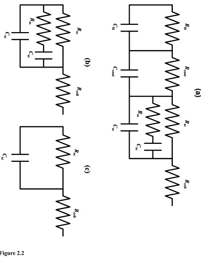
where kB is Boltzmann's constant, and Vbi denotes the built-in voltage of the junction. Figure 2.1 introduces the thermodynamic and kinetic parameters of a general
semiconductor/liquid junction. Ionized surface states and the Helmholtz layer are
explicitly considered in the energy diagram. The Galvani (or inner) potential, Ψο,
distributes itself over several regions of the semiconductor/liquid interface: (1) the
space-charge layer in the semiconductor, characterized by the surface potential, ΨS, and the space charge of electrons, holes and immobile donors and acceptors in the lattice, qsc , (2) a region of trapped charges in surface states, characterized by a surface state charge qss, (3) a Helmholtz layer formed by adsorbed ions or ionized surface groups and characterized by
the Helmholtz potential, q .VH and the adsorbed charge qad and last but not least (4) the double layer associated with ionic counter charge in the electrolyte, qel. Charge neutrality
[ ]
et S
( )
j E = − ⋅ ⋅q k A n⋅ (Eq. 2.2)
(
)
so
bi
s b
B B
exp exp
n
q V q E
n =n ⋅ − ⋅ k T ⋅ − ⋅ k T
Figure 2.1 Thermodynamic and Kinetic Parameters of a General Semiconductor/
Liquid Junction in the Presence of Ionized Surface States.
Ecb and Evb are the conduction and valence band edge, respectively. qVbi denotes the built-in-voltage at the point of zero charge, and ΦB the barrier height. At equilibrium the Fermi level of the semiconductor EF,sc equals the cell potential EF, A/A-. The inner
potential, Ψo, is distributed over the surface potential, ΨS, and the Helmholtz potential,
qVH. The barrier height for electron transfer can be changed by varying qVH (for instance through pH changes) and by changing EF, A/A-. If the junction is biased away
Figure 2.1
SC
liquid
E
cbE
vbE
F, SCqE
appE
F,A/A-(-)
(+)
(V
bi-E
ap p)
j(E)
E
greference
elect
ro
d
e
qE
F, S C E pHΨ
S∆G
0'
= -
Φ
BΨ
o io ni zed su rface s tat es qVHSC
liquid
E
cbE
vbE
F, SCqE
appE
F,A/A-(-)
(+)
(V
bi-E
ap p)
j(E)
E
greference
elect
ro
d
e
qE
F, S C E pHΨ
Scannot be measured directly, the most valuable information regarding the charge
distribution is obtained from differential capacitance measurements. The space-charge
region is a result of the equilibration of the two Fermi levels, EF,sc (Fermi level of the
semiconductor) and EF, A/A- (Fermi level of the redox couple in the electrolyte), which is
facilitated by the transfer of electrons between the bands of the semiconductor and the
redox couple in solution such that the net rate of electron transfer is zero at equilibrium.
The surface charge is larger than at equilibrium when an external bias is applied through
the back contact of the semiconductor with the result that a net current j(E) flows, see
Eq. 2.3. The thickness of the space-charge region is 100-1000 times the thickness of the
Helmholtz layer and the latter is insensitive to electron transfer and is solely determined
by the adsorption and desorption of ions. For metal oxide semiconductors, VH is found to be a function only of the pH of the solution, see Eq. 2.5.29, 33-35
According to Figure 2.1, the energy of a solvated electron with respect to a
reference electrode is given by its Galvani potential and thus the driving force for electron
transfer from n-ZnO(0001) to a redox couple in solution can not only be changed by
varying EF, A/A- but also by varying the pH of the supporting electrolyte. Both the Zn-rich
If the activity coefficient of ZnO- (aZnO-)and of Zn+ (aZn+) in Eq. 2.4 are assumed to stay constant, every pH unit change will result in a 55 mV shift in VH. Thus, as depicted in Figure 2.1, the band-edge position of a metal oxide semiconductor can be shifted with
respect to a fixed reference simply by varying the pH of the contacting aqueous
electrolyte.
Several attempts to derive expressions for the rate constant of heterogeneous
electron transfer between semiconductor electrodes and acceptor species in solution have
so far been undertaken. These attempts encompass simple collisional models30, 33 and an electronic coupling model adapting Marcus' treatment of electron transfer at the interface
ZnOH ZnO-+ H+
ZnOH Zn++ OH
-ZnOH ZnO-+ H+
ZnOH Zn++ OH
-H
H
H
2.3
2
o o o
ZnOH ZnOH ZnO ZnO H H
o o o
ZnOH ZnOH Zn Zn OH OH
ZnO
Zn
RT ln a
RT ln a
RT ln a
F V
RT ln a
RT ln a
RT ln a
F V
a
RT
RT
V
const
ln
pH
F
a
F
µ
µ
µ
µ
µ
µ
− − + +
+ + − −
− +
+
⋅
=
+
⋅
+
+
⋅
− ⋅
+
⋅
=
+
⋅
+
+
⋅
+ ⋅
⋅
=
+
⋅
−
⋅
of two immiscible liquids.12, 36 A final electronic coupling model for the rate law, Eq. 2.5,37 based on the Fermi Golden Rule uses the same formalism as Eq. 2.1:
In Eq. 2.5 βsc-1 is the coupling attenuation factor, l
sc the effective coupling length
in the semiconductor, λA,sc denotes the reorganization energy of the acceptor species near the semiconductor electrode36, 38 and dsc denotes the atomic density. The subscript 'sc' indicates parameters for a semiconductor electrode.
In order to obtain reliable rate constants from steady state j-E data for further
mechanistic studies, two stringent conditions must be met.10, 11 First, the rate law of Eq. 2.2 must be obeyed, which means that the observed rate must be first order in both the
acceptor concentration [A] and surface-electron concentration ns . While the first order dependence in [A] and ns can be qualitatively inferred from steady state j-E data, an independent and reliable method must be used in determining the value of ns. Secondly, the band-edges positions of the semiconductor electrode need to remain remain unchanged
with respect to a reference electrode when [A] is varied.
2.3 EXPERIMENTAL
2.3.1 Electrode Preparation
Hydrothermally grown n-type ZnO (0001) single crystals were purchased from
Atomergic Corp., Farmingdale NY (1 crystal: ZnO3) and Commercial Crystal
Laboratories, Inc. Naples, FL (2 crystals: ZnO1 and ZnO2). Electrochemical experiments (Eq. 2.5)
{ }
(
)
{ }
( )
(
)
[ ]
( )
12 2 13
3 ' -1 2 sc AB,sc sc sc B 2 B s F, A/A
2π 1
( ) β
6 π
4π
exp 4π
o
G
l
j E q H
d k T
qE k T A n E
reported by the manufacturer to be in the range of 10 to 104Ω cm. No data on the nature of the dopant or the mobility of the charge carrier were available from the supplier.
Due to the high cost of ZnO single crystals and due to their limited availability, a
polishing procedure was developed which allowed individual crystals to be reused for
multiple electrochemical experiments. The single crystal was removed from the sample
holder, cleaned, and mounted to a polishing fixture (South Bay Technology Inc., San
Clemente, CA), which exactly maintained the crystallographic orientation of the sample.
The mounting block was flattened with respect to the tungsten carbide linings of the
polishing fixture using #320 SiC paper (Struers, Denmark). The crystal was mounted to
the mounting block with the Zn-rich crystal face facing up using adhesive glue (softening
point of 80oC; Crystal Bound, South Bay Technology Inc., San Clemente, CA). The glue was allowed to solidify and a weight was placed on the crystal to ensure that the crystal
remained flush with respect the mounting block. Approximately 50 µm of the surface were removed by grinding with #800 SiC paper, followed by #1000 SiC paper and #1200
SiC paper (all Struers Denmark) and a 50 g weight. For polishing water-based diamond
suspensions of grain size 6, 3 and 1 µm (all South Bay Technology Inc., San Clemente, CA) were employed for approximately 60 min at each polishing grain size. After each
polishing step the surface was inspected microscopically and polishing was continued
until no further improvement of the surface quality was noticed. The final polishing step
was accomplished by chemically polishing the surface in a silica/KOH suspension
(50-100 nm, pH > 10, South Bay Technology Inc., San Clemente, CA) for at least 45 min. This
produced a damage-free surface. The orientation of the crystals were tested before and
after polishing with an X-ray Laue camera (Thomas Holzheu, CAMET Research Inc.,
Reports in the literature suggest a wide range of metals and alloys as suitable
ohmic contact materials for ZnO. Both electroplated indium20, 21 and Ga-In eutectic39 were tested and found to be suitable since they gave linear J-E curves when contacted with
ZnO. In all work described subsequently, the polished ZnO crystal was mounted to the
mounting block with the O-rich face pointing up using adhesive glue (Crystal Bound). The
surface was roughened using Precision Alumina powder 22 microns (South Bay
Technology Inc., San Clemente, CA). Ga-In eutectic, prepared by wetting an In shot (Alfa
Aesar 40338) with Ga ( Aldrich 26,326-5), was scratched onto approximately 80 % of the
oxygen-rich face of the crystals. Prior to the application of the ohmic contact, etching of
the O-rich face with concentrated phosphoric acid was necessary to improve the wetting of
the Ga-In eutectic. After removal from the crystal bound and cleaning in acetone and
isopropanol, a tinned copper wire (0.32 mm2 cross sectional area) was glued to the Ga-In eutectic using silver print (GC electronics 22-201, Rockford IL) and served as the
back-face contact.
The sample holder consisted of a glass tube (diam. 15 mm) into which the crystal
and the back-face contact were placed. The back-face contact was sealed by filling the
inverted glass tube with low-melting apiezon wax (softening point 120 oC) to a height of approximately 20 mm. The apiezon wax could be readily removed by dichloromethane.
The electrode area was defined by using black insulating paint (prepared by dissolving 3.6
g of Apiezon wax in 20 ml of hexanes) and it was made sure that all edges of the crystal
were covered with wax. The exact electrode area was determined photographically and
was typically 0.2-0.3 cm2.
Before experiments involving freshly polished ZnO crystals, the electrode was
etched in concentrated phosphoric acid (Aldrich 21,510-4) for seven min, rinsed with 18
MΩcm nanopure water (Barnstead NANOPure filter) and blown dry with N2(g). The
unwanted adsorbed species from the surface.
2.3.2 Electrochemical Measurements
All electrochemical experiments were carried out in a custom-made 4 neck round
bottom flask with a 29/42 ground glass joint to hold the ZnO electrode. The three 9/20
ground glass joints on the side held a EG&G bridging tube into each of which a standard
aqueous saturated calomel electrode (SCE, Fisher Scientific 13-620-52), a Pt gauze
counter electrode (with an apparent surface area approximately 20 times larger than the
area of the ZnO electrode), and a 2 mm diameter Pt working electrode (Bioanalytical
Systems, West Lafayette, IN), which was used to measure the cell potential and the
limiting currents, were immersed. The cell was designed such that a minimum amount of
solution (10 ml) could be used. Deaerated conditions were established by bubbling N2(g) or Ar(g) through the cell solution. All experiments involving Os-polybipyridyl compounds were carried out at 0 oC. Experiments involving the remaining redox compounds were carried out at room temperature.
After an electrode was etched, it was immersed in the supporting electrolyte for at
least 10 min before it was transferred to the electrochemical cell. This procedure proved
helpful in getting reproducible results. All solutions were stirred with a magnetic stir bar.
Nitrogen flow was terminated before the experiment to prevent bubbles from getting
trapped on the electrode surface. For each series of measurements, the short circuit current
of the ZnO-electrode was measured. J-E data and the open circuit potential were recorded
before an after the differential capacitance measurements. Solution potentials were
recorded before and after each experiment with respect to SCE and differed in no case by
Current-potential data were obtained with a Schlumberger Instruments
Electrochemical Interface Model SI1287. The scan rate was 20 mV/sec and usually three
cycles were employed. The current-potential data were corrected for the resistance of the
electrochemical cell, Rcell, and the concentration overpotential of the cell solution,
ηoverpot, see Eq. 2.6. The cell resistance was obtained from the high-frequency intercept of the impedance spectra, which was independent of the bias but differed from the bulk
resistance of the crystal. The concentration overpotential40 can be calculated from the mass transport limiting currents and used in the potential correction, see Eq. 2.7. However,
the concentration overpotential correction was in no case larger than 20 mV.
In Eq. 2.6 and Eq. 2.7 R denotes the gas constant, F is Faraday's constant, J is the
measured current (A), jJ-E the measured current density (A/cm2) and E the applied potential. The mass-transport-limited cathodic and anodic current densities, jA,lim and
jC,lim, respectively, were measured for each cell solution with a one-sided Pt-foil, which had approximately the same geometric surface area as the respective ZnO electrode. J-E
data were fitted to the full diode equation:32
where γ is the so-called diode quality factor, which is unity for the ideal case of a semiconductor/liquid contact that is first order in surface electron concentration.
Differential capacitance measurements were performed with a Schlumberger
Instruments Model 1260 Impedance Gain-Phase Analyzer interfaced to Model SI1287.
The Cdiff-2-E behavior of the semiconductor/liquid contact was recorded for DC biases
corr cell overpot cell
A,lim A,lim J-E overpot
C ,lim J-E C ,lim η
η
E E J R E J R
j j j
RT
ln ln
F j j j
= − ⋅ − ≈ − ⋅ − = − − − (Eq. 2.6) (Eq. 2.7) corr B 1 γ o qE
j j exp