N A N O E X P R E S S
Open Access
Preparation, characterization, and application of
titanium nano-tube array in dye-sensitized solar
cells
Shih-Yu Ho
1, Chaochin Su
1*, Chieh-Chung Cheng
1, Sasipriya Kathirvel
1, Chung-Yen Li
2and Wen-Ren Li
2*Abstract
The vertically orientated TiO2 nanotube array (TNA) decorated with TiO2 nano-particles was successfully fabricated by electrochemically anodizing titanium (Ti) foils followed by Ti-precursor post-treatment and annealing process. The TNA morphology characterized by SEM and TEM was found to be filled with TiO2 nano-particles interior and exterior of the TiO2 nano-tubes after titanium (IV)n-butoxide (TnB) treatment, whereas TiO2nano-particles were only found inside of TiO2nano-tubes upon titanium tetrachloride (TiCl4) treatment. The efficiency in TNA-based DSSCs was improved by both TnB and TiCl4 treatment presumably due to the increase of dye adsorption.
Keywords:TiO2, titanium tetrachloride, titanium (IV)n-butoxide, nano-tube, anodization, DSSCs
Introduction
Since O’Regan and Grätzel reported highly efficient TiO2-based dye-sensitized solar cells (DSSCs) in 1991, many attempts have been made to sensitize titanium dioxide (TiO2) nano-scale films. TiO2 nano-particulate films are typically preferred as they provide a high sur-face area for dye adsorption, leading to high photocur-rent conversion efficiency. Due to the three-dimensional transport path, TiO2 nano-particulate films brought higher electron recombination and met larger grain boundary among interconnected nano-particles. In this research, we have fabricated vertically orientated
one-dimensional nano-structure TiO2 nano-tube array
(TNA) by electrochemical anodization. The TNA-based DSSCs were expected to have a better performance than the nano-particulate-based DSSCs due to the better electron transportation and recombination property. However, due to the less surface area of TiO2nano-tube array, the efficiency of TNA-based DSSCs is still lower
than that of TiO2 nano-particle-based DSSCs.
Post-treatment of TNA by Ti precursors to form a TiO2
nano-particulate layers on TNA became a strategy
which could increase the TiO2 surface area for more dye adsorption. This research showed that the DSSCs fabricated by TNA after post-treatment by titanium tet-rachloride (TiCl4) and TiO2 nano-tubes after titanium (IV)n-butoxide (TnB) raised up the photocurrent con-version efficiency.
DSSCs have aroused intense interest over the past few years because they have been demonstrated to be able to achieve high solar-to-electric energy conversion effi-ciency with low-cost manufacture process and materials. In DSSCs, the photoelectrodes are made of porous semi-conductor layers chemisorbed with an organic sensitizer. When DSSCs are illuminated with sun light, the photo-electron of the sensitizer is ejected into the semiconduc-tor films and sent to the external circuit. The redox pairs in the electrolyte transport the holes from the oxi-dized dye molecules to the counter electrode to com-plete the electric cycle [1]. TiO2 is one of the most promising semiconductor materials in preparing the photoanodes for DSSCs due to its wide band gap char-acteristics and unique photoelectric properties [2]. TiO2 nano-particulate films are preferred as they provide a high surface area for dye adsorption, leading to high photocurrent conversion efficiency. The electron-collect-ing TiO2 layer in DSSCs is typically 10 to 15μm thick with a three-dimensional network of interconnected nano-particles. However, TiO2 nano-crystalline films
* Correspondence: [email protected]; [email protected]
1
Institute of Organic and Polymeric Materials, National Taipei University of Technology, Taipei, 10608, Taiwan, Republic of China
2
Department of Chemistry, National Central University, Chung-Li, 32001, Taiwan, Republic of China
Full list of author information is available at the end of the article
acquire long electron transport path and larger grain boundary between nano-particles [3,4]. This would hin-der the electron collection efficiency and limit the per-formance of DSSCs. It was proposed that one-dimensional TNA aligned perpendicular to photoanode substrate could enhance the electron transportation and, thus, lower the possibility of electron recombination with redox electrolytes, leading to the higher photo-to-electron conversion efficiency [3-5]. The TNA has been first prepared by Zwilling et al. using the electrochemi-cal anodization method [6]. The TNA morphology, including tube length, hole diameter, and wall thickness, can be systematically controlled by varying the anodiza-tion parameters, such as anodizaanodiza-tion potential, electro-lyte, and pH value [7,8]. Zhu et al. had investigated the dynamics of electron transport and recombination
prop-erties of the oriented TiO2 nano-tube structure in
DSSCs by frequency-resolved modulated photocurrent/ photovoltage spectroscopies and found the higher charge-collection efficiency and slower electron recom-bination in the TiO2 nano-tube-based DSSCs than the TiO2 nano-particle-based counterparts [3]. One of the reasons for improving the performance of the DSSCs is considered to be due to the increase of the amount of the dye adsorbed onto the TiO2 surface of photoelec-trodes in DSSCs. In order to increase the surface area of
TiO2 electrodes, post-treatment of TNA to form an
extra layer of TiO2 nano-particles has been applied [9-11]. In this work, we compared the effect of post-treatment of anodic TNA by different Ti-precursors on the TNA morphology and the resulting DSSCs performance.
Experimental details
Preparation, modification, and characterization of anodic TNA
Titanium foils with thickness of 0.25 mm (99.5% purity; Alfa Aesar, Ward Hill, MA, USA) were used for anodic growth of TNA. Titanium foils were first polished by sonication in chemical polishing solvent which con-tained nitric acid, ammonia fluoride, urea, ethanol, and hydrogen peroxide in 12:5:5:3:12 v/v ratio and rinsed subsequently with deionized (DI) water, acetone, and methanol. The anodization reaction was carried out in a two-electrode electrochemical cell with polished Ti foil (2 × 2.5 cm2) which served as the anode-working elec-trode and Pt foil (thickness 0.025 mm; Alfa Aesar) as the counter electrode. The separation between Ti elec-trode and Pt elecelec-trode was about 3.5 cm. The anodiza-tion electrolyte contains 0.3 wt% NH4F and 2 vol% H2O in ethylene glycol solution. The anodization was oper-ated under a constant potential of 60 V at low tempera-ture of 15°C with magnetic stirring. The reaction period
controlled the thickness of TiO2 nano-tube arrays.
Typically the TNA samples with tube length of approxi-mately 15 μm were obtained after 2 h of anodization process. It is evident that increasing the TNA length leads to the increase of short-circuit photocurrent den-sity due to the higher surface area available for dye adsorption. The TNA foils were then carefully washed with deionized water to remove the surface residual electrolyte in the nano-tube arrays. Such prepared TNA samples were then annealed at 450°C for 3 h with a heating rate of 1°C/min in order to transform the TNA from amorphous to anatase crystalline phase.
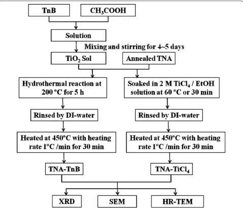
Figure 1 summarizes the procedures for
post-treat-ment of annealed TNA. The TiCl4-treated TNA
(TNA-TiCl4) was prepared from annealed TNA which was
soaked in 0.2 M TiCl4 solution (in ethanol) at 60°C for 30 min followed by heat treatment at 450°C for 30 min. The TnB-treated TNA (TNA-TnB) was prepared as
fol-lows: titanium (IV) n-butoxide (Ti(O-Bu)4, TnB)
(ACROS Organics, New Jersey, USA) was mixed with 2
M CH3COOH (pH = 2.5) at room temperature under
magnetic stirring for approximately 5 days until a homogeneous sol solution was obtained. The TiO2 sol and the annealed TNA were both transferred to a teflon-lined autoclave to perform the hydrothermal treatment at 200°C for 5 h. The Ti foil was then removed from the autoclave, rinsed with DI water, and heated at 450°C for 30 min to form TNA-TnB.
The surface morphology and crystal phase of TNA,
TNA-TiCl4, and TNA-TnB were investigated by
scan-ning electron microscopy (SEM) (SM6500F, JEOL Ltd., Akishima, Tokyo, Japan) and X-ray diffraction (XRD) (PANalytical X’Pert PRO, Almelo, The Netherlands), respectively. The results were confirmed by high-resolu-tion transmission electron microscopy (Hitachi H-7100, Hitachi Ltd., Chiyoda, Tokyo, Japan).
Dye-sensitized solar cell assemble and performance measurement
To fabricate DSSCs devices, three kinds of TNAs
including TNA, TNA-TiCl4, and TNA-TnB, served as
photoanodes, were combined with a transparent Pt counter electrode (cathode). The TNAs samples were
sensitized by dye molecules (3 × 10⁻⁴ M, N719 in a
mixed solvent of acetonitrile and tertbutyl acohol (volume ratio = 1:1)) for 24 h. The amount of dye adsorbed on TNA electrodes was determined by deso-rbing the N719 from TNAs surfaces into a solution of 0.1 M NaOH. The concentration of the adsorbed N719 was analyzed by UV-visible spectrophotometer (V-630, JASCO Corp., Easton, MD, USA). The Pt cathode was made by a ‘two-step dip coating’process developed by Wei et al. [12]. We have first prepared the poly-N -vinyl-2-pyrrolidone (PVP)-capped Pt nano-particles by dissol-ving PVP (M.W. = 8000) and H2PtCl6 (Pt precursor)
Hoet al.Nanoscale Research Letters2012,7:147 http://www.nanoscalereslett.com/content/7/1/147
into deionized water at room temperature and well stir-red until a light-yellow solution was obtained. A NaBH4 solution was then added drop by drop to the H2PtCl6 -PVP solution, and the solution quickly turned into a black color, indicating the formation of Pt nano-particles (Pt-PVP solution).
FTO glass (8Ω/sq., Solaronix SA, Aubonne VD, Swit-zerland) was pretreated by 1% ML-371 aqueous solution at room temperature for 1 min in order to increase adhesion between the PVP-capped Pt nano-particles and FTO surface. The ML-371-modified FTO substrate was then dipped into the Pt-PVP solution for 5 min and rinsed with deionized water followed by heat-treatment at 400°C for 5 h to remove completely the organic com-ponent and complete the preparation of counter electrode.
To assemble the DSSCs, the liquid electrolyte of 0.1 M lithium iodide, 0.05 M iodine (I2), 0.5 M 4-tert-butylpyr-idine, 0.5 M 1,2-Dimethyl-3-propylimidazolium iodide in acetonitrile was applied to the above-prepared Pt electrode which was then placed over the N719-coated TNAs electrodes. The edges of the cells sealed with a hot-melt film (Surlyn, 125 μm) and the electrolyte (I-/I2/ I3- redox couple) were injected into the space. The active cell area studied in this work is 0.25 cm2 (0.5 cm × 0.5 cm). The photoelectrochemical performance of the resultant solar cells were measured by back illumi-nated through the Pt counter electrode due to the non-penetration of light through the photoanode Ti metal substrate.
[image:3.595.59.538.88.498.2]The current (I)-voltage (V) characteristics were per-formed using a digital source meter (Keithley model Figure 1Procedures for post-treatment of annealed TNA. Fabrication flow chart of TNA-TiCl4and TNA-TnB. TNA, TiO2nano-tube array;
2400, Keithley Instruments Inc., Cleveland, OH, USA) with the TNA-based DSSCs devices under one-sun AM 1.5 irradiation from a solar simulator (300 W Xe light and filters, Oriel Instruments, Irvine, CA, USA) on a 0.25 cm2sample area.
Results and discussion
Formation and characterization of anodic titanium oxide nano-tube arrays
TiO2 electrode is one of the major concerns in DSSCs application. Since the TiO2 phase, morphology, and sur-face area of TiO2 films will affect the dye adsorption, electron transport, and electrolyte diffusion in the cell as well as the DSSCs performance. In this work, we have devised two kinds of Ti-precursor solutions to fabricate
TiO2 nano-particles decorated TNA on Ti substrates
which can serve as photoanodes for DSSCs device. Dur-ing the optimization stage of anodization process, the important roles of the anodization condition, including the thickness of Ti-foil (0.05-0.25 mm), temperature (15-30°C), anodization potential (20-60 V), reaction per-iod (10 min-24 h), and various kinds of F-containing electrolytes (HF, KF, and NH4F) in controlling the
thick-ness (length of TiO2 nano-tubes), homogeneity, and
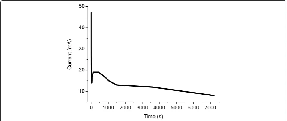
morphology of TNA were revealed. The data presented below were obtained with NH4F/H2O/ethylene glycol electrolyte solution after anodization procedure at 15°C for 2 h. Figure 2 shows a typical current-time plot recorded during the constant potential anodization pro-cess. Within the first few seconds, the current dropped drastically to a local minimum indicating the oxidation of Ti-foil to form surface pits acting as nucleation sites for tube formation [13]. Upon increasing the pit density,
the current increased to a maximum where the pit den-sity reached saturation. After further anodization, the current gradually decreased due to the continuously lengthen of TiO2nano-tubes. Such anodization behavior is commonly observed in the self-organized pore forma-tion process [14] in which the competiforma-tion between TiO2 oxide layer formation and dissolution of titanium progressed concurrently. Finally, the formation of verti-cally oriented TNA was achieved. The initially grown TNA was gray, which turned to yellow color after annealing at 450°C for 3 h.
Figure 3a shows the SEM images of the untreated TNA formed by anodizing a titanium foil with two types of magnification: 10,000× (top view) and 50,000× (side view, inset). The SEM image of lower magnifica-tion of TNA (Figure 3a) shows high porosity character of anodic TiO2 films with some nano-scale cracks. The higher magnification image of TNA (inset of Figure 3a) shows the self-organized TiO2 nano-tubes aligned den-sely with hexagonal close-packed arrangement. The
inner diameters of these TiO2 nano-tubes based on
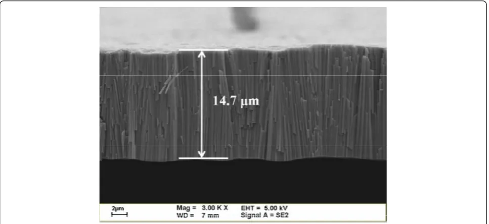
SEM images are in the range of 100-120 nm, and the wall thickness is approximately 10 nm. The thickness of TNA corresponding to the length of TiO2 nano-tubes is about 15μm obtained from the SEM cross section ana-lysis shown in Figure 4. It is consistent with other research works that high-aspect-ratio TiO2 nano-tubes can be fabricated with rapid growth rate by anodization [4,9,15].
Figure 3b, c shows the top-view SEM images of the decorated TNAs after post-treatment by TiCl4and TnB solution, respectively, with the corresponding side view images with higher magnification as shown in the inset
0 1000 2000 3000 4000 5000 6000 7000 10
20 30 40 50
C
ur
rent
(mA
)
[image:4.595.56.540.500.704.2]Time (s)
Figure 2Current-time plot of the constant potential anodization process. Current-time plot recorded during the constant potential anodization process.
Hoet al.Nanoscale Research Letters2012,7:147 http://www.nanoscalereslett.com/content/7/1/147
of Figure 3b, c. The length of TiO2 nano-tubes remains the same after different post-treatment. For both TiCl4
and TnB treated TNAs samples (denoted as TNA-TiCl4
and TNA-TnB), additional materials can be observed on the top of TNAs and inside the TiO2 nano-tubes. Yet,
[image:5.595.58.542.90.633.2]outside the TnB-treated TNA, the TiO2 nano-tubes
Figure 3SEM images of top view of (a) TNA, (b) TNA-TiCl4, and (c) TNA-TnB. The inset images are the side view of (a) TNA, (b) TNA-TiCl4,
and (c) TNA-TnB. TNA, TiO2nano-tube array; TNA-TnB, TiO2nano-tubes after titanium (IV)n-butoxide treatment; TNA-TiCl4, TiO2nano-tubes after
were apparently coated with an extra layer of TiO2 nano-particles. Transmission electron microscope
(TEM) experiments had been performed on TNA-TiCl4
and TNA-TnB samples detached from the Ti foil and dispersed on a copper grid. The bulk crystallites were observed (Figure 5a) inside TiO2 nano-tubes in the case
of TiCl4-treated TNA sample. In TnB-treated TNA,
bulk crystallites were observed both inside and outside the nano-tubes as shown in Figure 5b. The average inner diameter of TiO2 nano-tubes in TNA-TiCl4 and TNA-TnB after different post-treatment was about 85-120 nm based on TEM analysis which is consistent with SEM results.
XRD was used to confirm the crystalline phase of TiO2 nano-structure. Figure 6 shows the XRD patterns of (a) as-prepared TNA, (b) annealed-TNA, (c) TiCl4-treated TNA, and (d) TnB-treated TNA. The as-prepared TNA (before annealing) were amorphous (Figure 6a). Upon annealing to 450°C, the sharp anatase diffraction peaks appeared (Figure 6b) with crystal domain of approxi-mately 20 nm. After post-treatment by TiCl4and TnB, the XRD patterns remain the same for both TNA-TiCl4 and TNA-TnB, suggesting that the TiO2crystalline phase was not affected by post-treatment. The slight increase of TiO2crystal domain to 22 nm (for TNA-TiCl4) and 29 nm (for TNA-TnB) was due to the two times annealing at 450°C for post-treated TNAs samples.
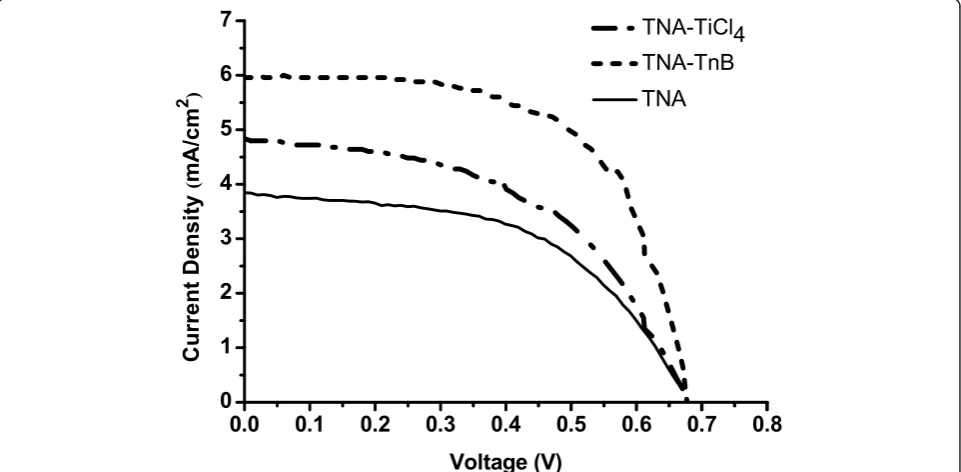
Application of anodic TNA electrodes to DSSCs and photoelectrochemical performance study
The above-prepared TiO2 nano-tube arrays (TNA,
TNA-TiCl4, and TNA-TnB) were used to fabricate the
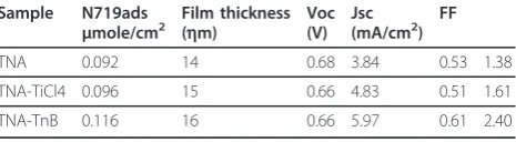
DSSCs for photoelectrochemical performance study. The results obtained from I-V curve measurements for N719-sensitized DSSCs under simulated AM 1.5 illu-mination is shown in Figure 7. The thickness of TNAs layers on Ti foil was fixed at approximately 15 μm. Table 1 lists the TNAs thickness, the amount of dye adsorbed on TNAs layers (N719ads), and photoelectric data of the DSSCs in Figure 7 including the open cir-cuit voltage, the short-circir-cuit photocurrent density (Jsc), the fill factor, and the photocurrent conversion efficiency (h). It is apparent that by post-treatment of the TNA, the performance of DSSCs was notably enhanced. The device based on the untreated TNA has shown the lowest Jsc (3.84 mA/cm2) and h (1.38%). This is due to the low surface area of the untreated TNA which uptakes less amount of dye molecules (0.092μmole/cm2). Higher efficiency and current den-sity of DSSCs device might be attributed to the higher amount of adsorbed N719 and the fast electron
trans-portation on TiO2 electrodes. As shown in Table 1,
TnB treatment assisted the higher dye adsorption
amount, raised from 0.092 to 0.116 μmole/cm2
(approximately 26% increase of N719ads), and Jsc also
raised from 3.84 to 5.97 mA/cm2 (approximately 55%
[image:6.595.57.541.89.311.2]increase of Js c). Both results lead to the efficiency improvement from 1.38% to 2.40% (approximately 74% increase of h). The significant increase of dye adsorp-tion is due to the increased surface area from the decorated TiO2 nano-particles on TNA, as clearly seen from the SEM images (Figure 3c). TEM images (Figure 5b) also vindicated the presence of bulk TiO2 crystal-lites inside and outside the TNA. The further increase Figure 4SEM cross sectional view of annealed-TNA. Mag, magnification; WD, width; EHT, extra high tension.
Hoet al.Nanoscale Research Letters2012,7:147 http://www.nanoscalereslett.com/content/7/1/147
of Jsc as well ash is attributed to the increase of TiO2 crystallinity of TNA-TnB, as evidenced by XRD. The
dye loading for TNA-TiCl4 sample is lower compared
to that of TNA-TnB because the TiO2 nano-particles
only subsist inside the nano-tubes. The slightly higher efficiency of TNA-TiCl4-based DSSCs compared to the
untreated TNA one is due to the better TiO2 crystalli-nity after two times annealing process. Variation in the performance of different devices might be due to the variations in the TiO2 tube length. Nevertheless, same trends were observed within each batch of device study.
Figure 5TEM images of (a) TNA-TiCl4and (b) TNA-TnB. TEM, transmission electron microscope; TNA, TiO2nano-tube array; TNA-TnB, TiO2
Conclusions
The decorated TNAs were successfully fabricated by anodization method followed by titanium precursor post treatment. The morphology of TNA without post-treat-ment was observed from SEM and TEM images, typi-cally approximately 15 μm length, approximately 100 nm diameter, and 10 nm wall thickness were achieved
[image:8.595.61.537.88.306.2]after 2 h reaction. TNA with titanium precursor treat-ment alters the morphology which was confirmed from the SEM and TEM images. In the case of TNA-TnB, TiO2 nano-particles were filled interior and exterior of the TiO2 nano-tubes, whereas TiO2 nano-particles were filled only inside the TiO2 nano-tubes in TNA-TiCl4 upon TiCl4 treatment. An XRD pattern clearly indicates
Figure 6XRD patterns of (a) as-prepared TNA, (b) annealed-TNA, (c) TiCl4-treated TNA, and (d) TnB-treated TNA. XRD, X-ray diffraction;
TNA, TiO2nano-tube array; TNA-TnB, TiO2nano-tubes after titanium (IV)n-butoxide treatment; TNA-TiCl4, TiO2nano-tubes after titanium
tetrachloride treatment; A, anatase diffraction peak.
0.0
0.1
0.2
0.3
0.4
0.5
0.6
0.7
0.8
0
1
2
3
4
5
6
7
TNA
TNA-TiCl4
TNA-TnB
Current De
nsi
ty
(
mA
/c
m
2 )
Voltage (V)
Figure 7Photocurrent-voltage characteristics of DSSCs made by TNA, TNA-TiCl4, and TNA-TnB. TNA, TiO2nano-tube array; TNA-TnB, TiO2
nano-tubes after titanium (IV)n-butoxide treatment; TNA-TiCl4, TiO2nano-tubes after titanium tetrachloride treatment.
Hoet al.Nanoscale Research Letters2012,7:147 http://www.nanoscalereslett.com/content/7/1/147
[image:8.595.58.539.465.701.2]that the TNA, TNA-TiCl4, and TNA-TnB were pure anatase phase after annealing process at 450°C. The photocurrent conversion efficiency of based,
TNA-TiCl4-based, and TNA-TnB-based DSSCs was 1.38%,
1.61%, and 2.40%, respectively. The results showed that
the DSSC efficiency in TNAs was enhanced by TiCl4
and TnB precursor post-treatment, presumably due to the increase of dye adsorption. The higher solar effi-ciency in TnB-doped DSSCs is due to the formation of extra layer of TiO2 nano-particles on TNA, leading to the higher amount of dye adsorption as well as higher photocurrent.
Abbreviations
DI: deionize; DSSCs: dye-sensitized solar cells; TEM: transmission electron microscope; TiCl4: titanium tetrachloride; TiO2: titanium dioxide; TNA:
titanium dioxide nano-tube array; TnB: titanium (IV) n-butoxide; SEM: scanning electron microscopy; XRD: X-ray diffraction.
Acknowledgements
This paper is a revised and expanded version of a paper entitled ‘Preparation, characterization and application of titanium nano-tube array in dye-sensitized solar cells’presented at IEEE International NanoElectronics Conference, Taiwan, June 21-24, 2011. We acknowledge the financial support from National Science Council of Taiwan, Republic of China (NSC 98-2113-M-027-003-MY3, NSC 100-2113-M-008-004-MY3).
Author details
1Institute of Organic and Polymeric Materials, National Taipei University of
Technology, Taipei, 10608, Taiwan, Republic of China2Department of Chemistry, National Central University, Chung-Li, 32001, Taiwan, Republic of China
Authors’contributions
The work presented here was performed in collaboration of all authors. SYH confirmed the results from the preliminary experiments and helped in writing the manuscript. CCC set up the anodization system and carried out the preliminary trails of anodization reaction. CS and WRL discussed the results and wrote the manuscript. SK and CYL proofread the manuscript and corrected the English. All authors read and approved the final manuscript.
Competing interests
The authors declare that they have no competing interests.
Received: 30 November 2011 Accepted: 21 February 2012 Published: 21 February 2012
References
1. Su CC, Hung WC, Lin CJ, Chien SH:The preparation of composite TiO2
electrodes for dye-sensitized solar cells.J Chin Chem Soc2010, 57:1131-1135.
2. O’Regan B, Grätzel M:A low-cost, high-efficiency solar cell based on dye-sensitized colloidal TiO2films.Nature1991,353:737-740.
3. Zhu K, Neale NR, Miedaner A, Frank AJ:Enhanced charge-collection efficiencies and light scattering in dye-sensitized solar cells using oriented TiO2nanotubes arrays.Nano Lett2007,7:69-74.
4. Park H, Kim WR, Jeong HT, Lee JJ, Kim HG, Choi WY:Fabrication of dye-sensitized solar cells by transplanting highly ordered TiO2nanotube
arrays.Sol Energy Mater Sol Cells2011,95:184-189.
5. Kuang D, Brillet J, Chen P, Takata M, Uchida S, Miura H, Sumioka K, Zakeeruddin SM, Grätzel M:Application of highly ordered TiO2nanotube
arrays in flexible dye-sensitized solar cells.ACS Nano2008,2:1113-1116. 6. Zwilling V, Aucouturier M, Darque-Ceretti E:Anodic oxidation of titanium
and TA6V alloy in chromic media. An electrochemical approach.
Electrochim Acta1999,45:921-929.
7. Alivov Y, Pandikunta M, Nikishin S, Fan ZY:The anodization voltage influence on the properties of TiO2nanotubes grown by
electrochemical oxidation.Nanotechnology2009,20.
8. Chen CC, Jehng WD, Li LL, Diau EWG:Enhanced efficiency of dye-sensitized solar cells using anodic titanium oxide nanotube arrays.J Electrochem Soc2009,156:C304-C312.
9. Yip CT, Mak CSK, DjurišićAB, Hsu YF, Chan WK:Dye-sensitized solar cells based on TiO2nanotube/porous layer mixed morphology.Appl Phys Lett
2008,92:589-593.
10. Roy P, Kim D, Paramasivam I, Schmuki P:Improved efficiency of TiO2
nanotubes in dye sensitized solar cells by decoration with TiO2
nanoparticles.Electrochem Commun2009,11:1001-1004.
11. Park SS, Eom SM, Seo DH, Shul YG:Preparation of highly ordered TiO2
nanotubes on Ti-foil for dye-sensitized solar cells.Res Chem Intermed
2010,36:77-82.
12. Wei TC, Wan CC, Wang YY:Poly (N -vinyl-2-pyrrolidone)-capped platinum nanoclusters on indium-tin oxide glass as counterelectrode for dye-sensitized solar cells.Appl Phys Lett2006,88.
13. Mor GK, Varghese OK, Paulose M, Grimes CA:Transparent highly ordered TiO2nanotube arrays via anodization of titanium thin films.Adv Funct Mater2005,15:1291-1296.
14. Yang DJ, Park H, Cho SJ, Kim HG, Choi WY:TiO2-nanotube-based
dye-sensitized solar cells fabricated by an efficient anodic oxidation for high surface area.J Phys Chem Solids2008,69:1272-1275.
15. Shankar K, Mor GK, Prakasam HE, Yoriya S, Paulose M, Varghese OK, Grimes CA:Highly-ordered TiO2nanotube arrays up to 220μm in length:
use in water photoelectrolysis and dye-sensitized solar cells.
Nanotechnology2007,18.
doi:10.1186/1556-276X-7-147
Cite this article as:Hoet al.:Preparation, characterization, and
application of titanium nano-tube array in dye-sensitized solar cells.
Nanoscale Research Letters20127:147.
Submit your manuscript to a
journal and benefi t from:
7Convenient online submission 7Rigorous peer review
7Immediate publication on acceptance 7Open access: articles freely available online 7High visibility within the fi eld
7Retaining the copyright to your article
[image:9.595.58.291.101.165.2]Submit your next manuscript at 7 springeropen.com Table 1 The I-V characterization of TNAs-based DSSCs
Sample N719ads
μmole/cm2
Film thickness (hm)
Voc (V)
Jsc (mA/cm2)
FF
TNA 0.092 14 0.68 3.84 0.53 1.38
TNA-TiCl4 0.096 15 0.66 4.83 0.51 1.61