International Journal of Emerging Technology and Advanced Engineering
Website: www.ijetae.com (ISSN 2250-2459, ISO 9001:2008 Certified Journal, Volume 3, Issue 2, February 2013)
279
Design And Analysis Of Low Power Single Edge Triggered
D Flip Flop Based Shift Registers
Mathan. N
1, T. Ravi
2,
E. Logashanmugam
3 1II Year M.Tech, VLSI Design, Sathyabama University, Chennai.
2 Asst. Professor, 3Head of the Department, Department of ECE, Sathyabama University, Chennai.
Abstract—In this paper, analysis of average power, delay
and power delay product is done for various shift registers(SISO, SIPO, PISO and PIPO) Low power flip-flops are crucial for the design of low-power digital systems. As Metal Oxide Semiconductor Field Effect Transistor (MOSFET) devices are scaled down to nanometer ranges, Complementary MOS (CMOS) circuit’s total Power consumption has a new definition. Due to integration of millions of components and shrinking process technology, nowadays leakage power tends to play a major role in total power consumption. In this paper, the shift registers are designed with various frequencies and their performance is analyzed.
Keywords—CMOS, MOSFET, D Flip Flop, Shift Registers,
Single Edge Triggered flip flop , Power Consumption, Delay, Power Delay Product.
I. INTRODUCTION
The system on chip (SoC) design will integrate hundreds of millions of transistors on one chip, whereas packaging and cooling only have a limited ability to remove the excess heat [1]. So large amount of heat should not be dissipated. Thus low power design is the need of today's integrated systems. The low power design is also needed for the applications operated by batteries such as pocket calculators, wrist watches, mobile phones, laptops etc. It is important to prolong the battery life as much as possible. Flip flops are the basic storage elements used extensively in all kinds of digital designs. As the feature size of CMOS technology process shrinks according to Moore’s Law, designers are able to integrate more transistors onto the same die. The more transistors there are the more switching and the more power dissipated in the form of heat or radiation. Heat is one of the most important packaging challenges in this era; it is one of the main drivers of low power design methodologies and practices. Another mover of low power research is the reliability of the integrated circuit. More switching implies higher average current is flowing and therefore the probability of reliability issues occurring rises.
The most important prime mover of low power research and design is our convergence to a mobile society. We are moving from desktops to laptops to handhelds and smaller computing systems. With this profound trend continuing, and without a matching trend in battery life expectancy, the more low power issues will have to be addressed. This entails that low power tools and methodologies have to be developed and adhered to. The current trends will eventually mandate low power design automation on a very large scale to match the trends of power consumption of today’s integrated chips.[9] In this paper the background information about flip-flop design and characteristics are analyzed.
II. SINGLE EDGE TRIGGERED D-FLIPFLOP
International Journal of Emerging Technology and Advanced Engineering
Website: www.ijetae.com (ISSN 2250-2459, ISO 9001:2008 Certified Journal, Volume 3, Issue 2, February 2013)
[image:2.612.80.259.136.236.2]280 FIG.1 LOW POWER SET D FLIP FLOP
III. SHIFT REGISTERS
Shift registers are a type of sequential logic circuit, mainly for storage of digital data. They are a group of flops connected in a chain so that the output from one flip-flop becomes the input of the next flip-flip-flop. Most of the registers possess no characteristic internal sequence of states. All flip-flop is driven by a common clock. There are different kinds of shift registers.
* Serial in serial out shift register. *Serial in parallel out shift register. *Parallel in parallel out shift register. *Parallel in serial out shift register.
The storage capacity of a register is the total number of bits (1 or 0) of digital data it can retain. Each stage (flip flop) in a shift register represents one bit of storage capacity. Therefore the number of stages in a register determines its storage capacity.
A. Serial In Serial Out(SISO) Shift Register
[image:2.612.328.561.185.312.2]The Serial In Serial Out (SISO) shift register accepts data serially (one bit at a time on a single line). It produces the stored information on its output also in serial form. And the basic Serial In Serial Out (SISO) shift register is shown in Fig 2.
FIG 2: SERIAL IN-SERIAL OUT SHIFT REGISTER
B. Serial In Parallel Out(SIPO) Shift Register
This configuration allows conversion from serial to parallel format. Data input is given serially, as described in the SISO section above.
Once the data are stored, each bit appears on its respective output line, and all bits are available simultaneously. And the basic Serial In Parallel Out (SIPO) shift register is shown in Fig 3.
FIG 3: SERIAL IN-PARALLEL OUT SHIFT REGISTER
C. Parallel In Serial Out(PISO) Shift Register
This configuration has the data input on lines D1 through D4 in parallel format. To write the data to the register, the Write/Shift control line must be held LOW. To shift the data, the W/S control line is brought HIGH and the registers are clocked. The arrangement now acts as a PISO shift register, with D1 as the Data Input. However, as long as the number of clock cycles is not more than the length of the data-string, the Data Output, Q, will be the parallel data read off in order. And the Parallel In Serial Out is shown in Fig 4.
FIGURE 4: PARALLEL IN SERIAL OUT SHIFT REGISTER
D. Parallel In Parallel Out(PIPO) Shift Register
[image:2.612.65.272.558.644.2]International Journal of Emerging Technology and Advanced Engineering
Website: www.ijetae.com (ISSN 2250-2459, ISO 9001:2008 Certified Journal, Volume 3, Issue 2, February 2013)
281
The D's are the parallel inputs and the Q's are the parallel outputs. Once the register is clocked, all the data at the D
inputs appear at the corresponding Q outputs
simultaneously.
FIGURE 5: PARALLEL IN PARALLEL OUT SHIFT REGISTER
IV. SIMULATION RESULT
[image:3.612.331.552.98.635.2]To evaluate the performance, shift registers discussed in this paper are designed using 130-nm CMOS technology. All simulations are carried out using HSPICE simulation tool at nominal conditions with different range of frequencies from 100MHz to 1GHz. The simulated waveform of various shift register is shown in Fig.6,7,8 & 9.
[image:3.612.59.282.176.322.2]FIG. 6 :OUTPUT WAVEFORM FOR SISO
FIG.7 :OUTPUT WAVEFORM FOR SIPO
FIG. 8 :OUTPUT WAVEFORM FOR PISO
[image:3.612.60.278.452.601.2]International Journal of Emerging Technology and Advanced Engineering
Website: www.ijetae.com (ISSN 2250-2459, ISO 9001:2008 Certified Journal, Volume 3, Issue 2, February 2013)
282
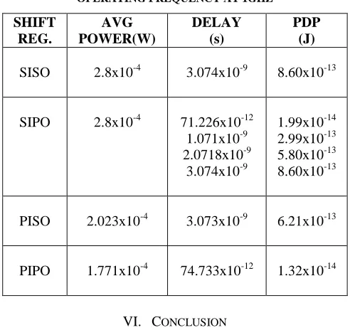
V. PERFORMANCE ANALYSIS
[image:4.612.321.567.137.369.2]The performance of the shift registers is evaluated by comparing the average power, delay and power delay product (PDP). In general, a PDP based comparison is appropriate for low power portable systems in which the battery life is the primary index of energy efficiency. The following tables from TABLE 1 to TABLE 3 furnished the performance parameters for different range of frequencies from 100MHZ to 1GHZ.
TABLE 1
OPERATING FREQUENCY AT 100MHZ
TABLE 2
OPERATING FREQUENCY AT 500MHZ
TABLE 3
OPERATING FREQUENCY AT 1GHZ
SHIFT REG. AVG POWER(W) DELAY (s) PDP (J)
SISO 2.8x10⁻⁴ 3.074x10⁻⁹ 8.60x10⁻¹³
SIPO 2.8x10⁻⁴ 71.226x10⁻¹²
1.071x10⁻⁹ 2.0718x10⁻⁹ 3.074x10⁻⁹ 1.99x10⁻¹⁴ 2.99x10⁻¹³ 5.80x10⁻¹³ 8.60x10⁻¹³
PISO 2.023x10⁻⁴ 3.073x10⁻⁹ 6.21x10⁻¹³
PIPO 1.771x10⁻⁴ 74.733x10⁻¹² 1.32x10⁻¹⁴
VI. CONCLUSION
In this paper, we have designed low power single edge triggered D-FF based shift registers design in 130nm CMOS technology. The shift registers are simulated with different operating frequencies ranging from 100MHz to 1GHz.The shift registers design is efficient by comparing average power, delay and power delay product. Hence by performance analysis the low power single edge triggered D-FF based shift registers design is efficient for low power applications.
REFERENCES
[1 ] Dr. Sunil P Khatri and Sivakumar Ganesan," A Modified Scan-D Flip-flop Design to Reduce Test Power".
[2 ] Ahmed Sayed and Hussain Al- Asaad." A New low power high performance flip-flop".
[3 ] Mounir ZID, Carlo PISTRITTO, Rached TOURKI and Alberto SCANDURRA," A New Low- Power N Fold Flip-Flop With Output Enable".
[4 ] Hongli Gao Fei Qiao Dingli Wei Huazhong Yang," A Novel Low-Power and High-Speed Master-Slave D Flip- Flop".
[5 ] Jinn-Shyun Wung, Po-Hui Yung, "A Pulse- Triggered TSPC Flip-Flop for High-speed Low-Power VLSI Design Applications". [6 ] Manoj sharma, Dr Arti Noor." An Area and Power Efficient design
of Single Edge Triggered D-Flip Flop".
[7 ] D.Markovi, B.Nicolic and R.W Borderson,"Analysis and design of low energy flip flops".
[8 ] Imran Ahmed Khan, Owais Ahmad Shah and Mirza Tariq Beg," Analysis of Different Techniques for Low Power Single Edge Triggered Flip Flop".
[9 ] R. Udaiyakumar, K. Sankaranarayan, Certain Investigations on Power Dissipation in various Nano-Scale CMOS D Flip- Flop Structures". SHIFT REG. AVG POWER(W) DELAY (s) PDP (J)
SISO 2.6x10⁻⁵ 30.83x10⁻⁹ 8.01x10⁻¹³
SIPO 2.6x10⁻⁵ 71.26x10⁻¹²
10.828x10⁻⁹ 20.824x10⁻⁹ 30.83x10⁻⁹ 1.85x10⁻¹⁵ 2.81x10⁻¹³ 5.41x10⁻¹³ 8.01x10⁻¹³
PISO 1.153x10⁻⁵ 30.071x10⁻⁹ 3.46x10⁻¹³
PIPO 1.552x10⁻⁵ 73.225x10⁻¹² 1.13x10⁻¹⁵
SHIFT REG. AVG POWER(W) DELAY (s) PDP (J)
SISO 1.367x10⁻⁴ 6.072x10⁻⁹ 8.30x10⁻¹³
SIPO 1.367x10⁻⁴ 71.08x10⁻¹²
2.070x10⁻⁹ 4.070x10⁻⁹ 6.072x10⁻⁹ 9.7x10⁻¹⁵ 2.8x10⁻¹³ 5.56x10⁻¹³ 8.30x10⁻¹³
PISO 9.158x10⁻⁵ 6.073x10⁻⁹ 5.56x10⁻¹³
[image:4.612.41.289.253.690.2]International Journal of Emerging Technology and Advanced Engineering
Website: www.ijetae.com (ISSN 2250-2459, ISO 9001:2008 Certified Journal, Volume 3, Issue 2, February 2013)
283
[10 ]Vladimir Stojanovic, Vojin Oklobdzija and Raminder Bajwa," Comparative Analysis of Latches and Flip- Flops for High-Performance Systems".
[11 ]Vladimir Stojanovic and Vojin G. Oklobdzija," Comparative Analysis of Master–Slave Latches and Flip- Flops for High-Performance and Low-Power Systems.
[12 ]Ch. Daya Sagar and T. Krishna Moorthy," Design of a Low Power Flip-Flop Using MTCMOS Technique".
[13 ]A.G.M. Strollo, E. Napoli, D. De Caro, "New Clock- Gating Techniques for Low-Power Flip- flops".
[14 ]Manisha Sharma, K. G. Sharma, Tripti Sharma, "SET D-Flip Flop Design for Portable Applications".
[15 ]S. Jagannathan, T. D. Loveless, B. L. Bhuva, S.-J. Wen, R. Wong, M. Sachdev, D. Rennie, and L. W. Massengill., "Single-Event Tolerant Flip-Flop Design in 40-nm Bulk CMOS Technology" [16 ]Ahmed Sayed and Hussain Al- Asaad,"Survey And Evaluation Of
Low-Power Flip-Flops".
Mathan. N was born in Neyveli, Tamilnadu, India in 1989. He received his Bachelor Degree in Electronics and Communication Engineering from Anna University, Chennai in the year 2010.Currently he is doing M.Tech VLSI DESIGN in Sathyabama University, Chennai. His interested areas are Nano Electronics, VLSI Design, Low Power VLSI Design and Advanced Digital System Design. He has Research publications in International Journals.
T. Ravi was born in Namakkal, Tamilnadu, India in 1978. He received his Bachelor Degree in Electrical and Electronics Engineering from Madurai Kamaraj University in the year 2001, Master Degree in Applied Electronics from Sathyabama Deemed University in the year 2004. Currently he is doing Ph.D in Sathyabama University. He is working as Assistant Professor in Department of ECE in Sathyabama University. His interested areas of research are Nano Electronics, VLSI Design, Low Power VLSI Design and Mixed Signal circuits. He has Research publications in National / International Journals /Conferences. He is a member of VLSI Society of India.