Journal of Chemical and Pharmaceutical Research, 2014, 6(6):2105-2109
Research Article
ISSN : 0975-7384
CODEN(USA) : JCPRC5
Implementation and design of power amplifier module with momentum
Kang Li and Dai Jianguang
Department of Electrical Engineering and Automation, Institute of Technology of Luoyang,
Henan, China
_____________________________________________________________________________________________
ABSTRACT
Power amplifier modules are key components of RF communication systems. This paper describes the implementation of a 1.95 GHz power amplifier module. The design of micro-strip matching circuit in modules and methods of momentum simulation are described. The test results show that the module features excellent performance, satisfying requirements of the design.
Key words: Power amplifier module; Micro-strip; matching circuit; Momentum simulation
_____________________________________________________________________________________________
INTRODUCTION
Power amplifier modules that are the key device in modern wireless communications are highly applied in such systems as radar、navigation、electronic countermeasures and satellite communications. PA with the high efficiency、
high output power、high linearity and high gain can be broadly applied in the fields like digital transmitter mobile
communication base station and military technology[1-3]. The 3G and 4G technology set the needs for far better performance of the RF microwave PA in order to satisfy the needs for the real application in Broad Band、
efficiency、output power and linearity. The L waveband, used as a universal waveband, is a carrier for many systems.
So the device and module on this waveband is extensively used.
THE DESIGN OF THE MATCHING CIRCUIT
The matching circuit is a key link in the design of PA. Inputting matching circuit is mainly for accomplishment of the wider broadband and higher power gain while outputting matching circuit is mainly for accomplishment of high work efficiency and power delivery. When designing the network of the matching circuit, the designers should concern the simplexes of the circuit, the width of the waveband and the category and the adjustability of it. Comprehensively, a kind of mingled matching circuit network of micro-strip line and discrete component is adopted in this paper[4-5]. The micro-strip line, a popular plane transmission line recently, is processed through Gerber and easily integrated with other wave devices passive and active. The characteristic resistance value of the micro-strip line is decided by the parameters of width, the thickness and base materials of base plate, the thickness of the copper foil and so on. The characteristic resistance value is decided by the width only if the materials are sure. According to the formula:
0
[1.393 / 0.667 ln( / 1.444)]
f
eff
Z Z
w h w h
ε
=
+ + + (1)
Computing the width W, h in the formula is the thickness of the base
1 1
(1 12 )
2 2
r r
eff
w h
ε ε
0 0 376.8 f Z µ ε
= = Ω (3)
In order to minimize the energy loss in the signal transmission, the inputting and outputting signal connecting line matches with the front and back grades through the 50 Ohm characteristic impedance. The matching circuit is realized by the ADS simulation software, adopted the load-pull to reach the best load impedance in the PA module.
[image:2.595.183.430.252.427.2]The principle of the load-pull is that under the stimulation of the large-signal level the PA tests the outputting power through the successive load changes, diagramming the curve of the equal-gain and the equal-power in the Smith diagram, which design accurately through the election of the proper output impedance. The load-pull can reach the best load resistance value precisely to simulate large-signal PA characters such as the output rate, gain, additional power and the IMD3 and IP3[6]. Comprehensive concern on the best load resistance value through the load-pull in figure 1,ZL=6.507+j*5.791Ohm and the best origin resistance value ZS=1.89-j*5.599Ohm which both are .Used in
the matching network design.
m3 real_indexs11= surface_samples=0.772 / 166.564 imag_indexs11=0.179487 impedance = 6.507 + j5.791
-0.751
real_indexs11 (-0.999 to -0.001)
s u rf a c e _ s a m p le s m3 R h o _ In _ F u n d
(0.000 to 0.000)
R h o _ In _ F u n d [i m a g _ in d e x ,r e a l_ in d e x ] m3 real_indexs11= surface_samples=0.772 / 166.564 imag_indexs11=0.179487 impedance = 6.507 + j5.791
-0.751
48.75
PAE, %
6.507 + j5.791
Impedance at marker m3
36.17
Pow er Delivered (dBm) Move Marker m3 to select load impedance value. Corresponding PAE, delivered pow er, input reflection coefficient and impedance values w ill be updated.
Simulated Load Impedances and Input Reflection Coefficients
0.93 / 1.64E2
1.95 + j7.06
Input Reflection Coefficient
Input Impedance
Fig. 1:the best load resistance value from load-pull
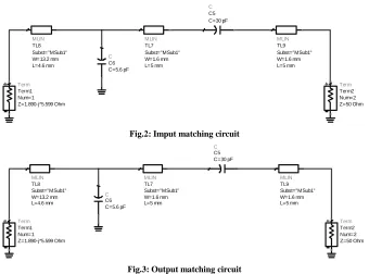
[image:2.595.136.476.452.704.2]MLIN TL8 L=4.6 mm W=13.2 mm Subst="MSub1" Term Term1 Z=1.890-j*5.599 Ohm Num=1 MLIN TL9 L=5 mm W=1.6 mm Subst="MSub1" Term Term2 Z=50 Ohm Num=2 C C6 C=5.6 pF MLIN TL7 L=5 mm W=1.6 mm Subst="MSub1" C C5 C=30 pF
Fig.2: Imput matching circuit
MLIN TL7 L=5 mm W=1.6 mm Subst="MSub1" C C5 C=30 pF Term Term2 Z=50 Ohm Num=2 MLIN TL9 L=5 mm W=1.6 mm Subst="MSub1" MLIN TL8 L=4.6 mm W=13.2 mm Subst="MSub1" Term Term1 Z=1.890-j*5.599 Ohm Num=1 C C6 C=5.6 pF
plate copper foil is 0.035mm. All the procession of the matching is finished in the Smith diagram, and fully take advantages of the Q to design the waveband needed, and the consequential impute and output matching circuit separately are figure 2 and 3:
THE MOMENTUM DESIGN OF PA
Schematic circuit diagram is simulated under completely ideal conditions, while there is a considerable gap between the real production of circuit board and its theory. Thus, this needs to consider the effects of the factors such as interference coupling. So the domain needs to be further simulated. ADS domain adopts momentum to simulate in electromagnetic way [7]. The simulation result is more accurate than in the schematic diagram.
Agilent momentum is a leading three-dimension EM plane emulator, which can be used to model and analyze for passive circuit and can simulate any design of geometric structure(including multilayered structure) and can adopt MOM technical and accurately-simulate complex electromagnetic effect(including coupling and parasitism). The exact electromagnetic simulation can support designers improving design performance of RF/MMIC RF/high speed PCB RF/SIP and ANT, in addition, it ensures that the products can achieve technical indicator .momentum combine full-wave static electromagnetism solver to use for RF passive device and high frequent interconnection and parasitic modeling [8]. Its high efficient reseal and self-adaptive frequency sampling and NLOGN solver can shorten time and can simulate complex electromagnetic effect; including skin effect subtract effect heavy metal and more dielectric effect. Transfer matching network into momentum element for circuit design, then combine biasing circuit to get the circuit of PA module. As shown in figure 4
V_DC
SRC2
Vdc=28.0 V
V_DC
SRC1
Vdc=2.8 V
Term
Term4
Z=50 Ohm Num=4
Term
Term3
Z=50 Ohm Num=3
C
C8
C=30 pF
C
C1
C=30 pF
SCH2
SCH2_1
ModelType=Dataset
Ref
TL11
TL7 TL8 TL9 TL10
TL13 Bend3
TL12
TL5
TL6 TL4
TL2 Bend2 TL1
G ap1 G ap2
C
C14
C=1.4 pF {-t}
C
C4
C=30 pF
FSL_MRF_MET_MODEL
MRF2
CTH=-1 RTH=-1 TSNK=25 MODEL=MW6S004N
C
C9
C=30 pF
C
C10
C=1.7 pF {t}
C
C16
C=0.5 pF {t}
C
C17
C=2.5 pF {t}
C
C11
[image:3.595.136.475.307.436.2]C=3.6 pF {t}
Fig.4: momentum design drawing of PA
Adopt single-tone harmonic balance method to simulate circuit. Set drain voltage :28V grid voltage 2.8v
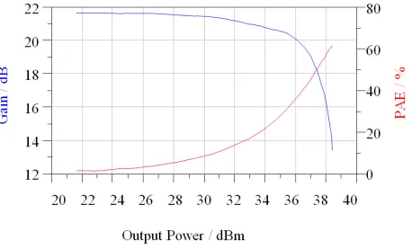
[image:3.595.193.422.514.653.2]operating frequency 1.95GHZ scanning power 0~25dbm simulation result as shown in figure 5.It can be seen from figure that it meets the design requirement, output power of comprehension point of 1db circuit is about 36dbm,gain is about 20db PAE is about 40%
Fig.5: relation curve between output power and gain and output
Fig.6: curve relation between IMD3 and output power
TEST RESULT
According to momentum artificial circuit which processes module, through repeated debugging, then test it .Test instrument employs new vector network analyzer of Agilent company-PNA-XM5241A. At last get the gain curve, as shown in figure 6.it can be seen that the central frequency in 1.95GHZ of small-signal gain is 19.7db, which matches with simulation curve well. Figure 7 is curve of IM3 module, and the curve show in the frequency range 1.9GHz~2.1GHz.while,it has a good linearity with IM3 below -31db
Fig.7: Gain curve of PA
method momentum improves design of pa from simple circuit level to physical level, and the result is more accurate. Momentum run through all the design process, Using Circle diagram to Conjugate match input and output impedance, making full use of Q circle to design bandwidth, and getting the high-performance PA module. Test result indicates that output power of 1db is about 36dbm,PAE is approximant to 40%,the gain of central frequency in 1.90GHz is about 20db,the gain in the 1.8GHz~2.1GHz frequency band range hold above 15db, while IM3 below-31db.the outcome of test and simulation match well and it verify design correctness.
REFERENCES
[1] Yuna J. Television Technology. V.15,n.5, pp.56-62, May, 2006. [2]Hu N, Zhou Z. Television Technology.V.13,n.3,pp.25-31,March,2004.
[3]Shi C, Quan N. IEEE Microwarve and Wireless Components Letters. V.21, n.1,pp.31-33, January,2011. [4]Li X, Chen W. Asia Pacific Microwave Conference. PP.654-657,2010.
[5]James B. IEEE Trans on Plasma Science. V.36, n.3, pp.29-38, March, 2008.
[6]Fagotti R, Cidronali A. IEEE Microwave and Wireless Components Letters. V.20, n.1, pp. 56-60. January,2010. [7]Salcedo S, Xin Y. IEEE Transactions on Systems.V.3,n.5, pp.2343-2353, May, 2004.
[8]An W, Shao F. Computer and Mathematics With Applications. V.57,n.4,pp529-539, April, 2009.