DYNAMIC VOLTAGE RESTORER USING THREE PHASE
AC-AC CONVERTER
1V.JAYALAKSHMI, 2 DR.N.O.GUNASEKHAR
1
Research Scholar, Bharath University, Chennai, Tamil Nadu, India.
2
Professor, Eswari Engineering College, Chennai, Tamil Nadu, India.
E-mail: [email protected], [email protected]
ABSTRACT
In this paper, Dynamic Voltage Restorer using Z source AC - AC converter has been proposed to mitigate the voltage sag/ swell. Dynamic Voltage Restorer (DVR) is an effective custom power devices used to protect the sensitive loads against voltage sag and swell. The three phase Z source AC-AC converter has been employed to perform the direct AC/AC conversion. The Z source network can produce any desired output AC voltage, which is a greater or less voltage than the line voltage. Hence it enhances the voltage restoration capability of DVR. The gating pulses for the bidirectional switch are generated using sinusoidal PWM technique and its associated circuitry. This proposed topology is simulated under voltage sag /swell using Matlab / Simulink and the simulation results are presented to show that the system effectively compensates the voltage sag/ swell.
Keywords: Dynamic Voltage Restorer, Voltage Sag, Voltage Swell, Z- Source AC-AC Converter.
1. INTRODUCTION
Power quality issues like voltage sag, voltage swell, transients and harmonics have become major concern in most industries today, due to the increased application of sensitive loads [1]. These power quality problems can cause malfunctioning of sensitive equipments and process interruptions. Distribution system is mainly affected by voltage sag /swell power quality issue. Such voltage sag / swell have a major impact on the performance of the microprocessor-based loads as well as the sensitive loads [2]. Dynamic Voltage Restorer (DVR) is one of the most important custom power devices, which is connected in series with the distribution system to mitigate the power quality problems [3].It is connected in series between the supply and the critical load. The basic function of the DVR is to inject a controlled voltage into the system in order to regulate the load voltage.
Generally, DVR is composed of series Voltage Sources Inverter (VSI) an energy storage element, LC filter, and a series injection transformer. In many references, the VSI is greatly used in DVR due to their appropriate output voltage with low harmonic level [4][5]. This VSI is fed from a dc voltage source with a capacitor in parallel to absorb the high-frequency ripple. It has six switches with a
freewheeling diode in parallel with each of them. It has several limitations as listed below:(i) the output voltage range is limited to 1.15 times half the dc source voltage (ii) it has relatively low efficiency, due to switching losses and EMI generation and (iii) the upper and lower devices of the same leg cannot be fired on the same time because a short circuit (shoot through) will occur and destroy the devices [6,7]. To overcome these limitations, a new Z source AC-AC converter is proposed in this paper. The impedance network consists of two equal inductors and capacitor connected in X shaped configuration[8] .The unique features of three-phase AC-AC Z source converter is that it transfers the energy directly from AC to AC and the output voltage can be bucked or boosted to a desired magnitude[9,10]. Hence the Z source AC-AC converter is used in DVR to compensate the voltage sag/ swell.
2. DVR USING Z SOURCE AC-AC CONVERTER
Figure 1 DVR Using Z Source AC-AC Converter
Figure 1 shows the proposed DVR using Z source AC-AC converter. It consists of Z source AC-AC converter, Lf Cf filter, Injection transformer
and Load.
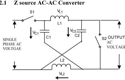
[image:2.595.89.292.384.515.2]2.1 Z source AC-AC Converter
Figure 2 Z source AC- AC converter
The Z source AC-AC converter consists of two bidirectional switches and Z source network as shown in Figure 2. The Z source network consists two equal inductors L1,L2 and two equal capacitors
C1,C2 connected in X shape. It acts as energy
storage/filtering element and provides buck-boost function. Each bidirectional switches consists of two IGBTs connected in common emitter mode back to back and the two diodes provide reverse blocking capability. These two bidirectional switches are turned on and off in complement Pulse Width Modulation (PWM) signal. i.e. switch S1 is turned on with (D) and switch S2 is turned on with (1-D). By controlling the duty ratio D the desired output voltage can be obtained. The AC-AC converter is connected in shunt series configuration. The Z source AC-AC converter can directly convert AC voltage into AC voltage with variable
amplitude. The switching frequency of PWM signal is much higher to have the smaller value of capacitor and inductor of Z source network. This converter has the following features such as the output voltage can be bucked/boosted and be in phase/out-of-phase with the input voltage reducing inrush and harmonic current. When the output voltage is boosted and in-phase with the input voltage, the DVR compensates voltage sag. When the output voltage is bucked and out of phase with the input voltage, the DVR compensates the voltage swell.
2.2 Filter Unit
This unit consists of inductor (Lf) and
capacitor (Cf). It is used to reject the switching
harmonics generated due to the nonlinear characteristics of switching devices. The filter can be placed either the high-voltage side or low voltage side of the injection transformer
2.3 Injection Transformer
The Injection / Booster transformer is a specially designed transformer to limit the coupling noise and transient energy from primary side to the secondary side. The high voltage winding is connected in series with the distribution line and the low voltage winding is connected in series with the power circuit. The basic functions of the injection transformer are : (i) It couples the injected compensating voltage generated by the AC-AC converter to the supply voltage (ii) it isolates the DVR circuit from the distribution network.
3. OPEARTION OF DVR
This proposed DVR operates in the following three modes based on the magnitude of error voltage.
3.1 Injection mode
The DVR operates in this mode as soon as the voltage sag/swell is detected. In case of voltage sag, the DVR injects an equal positive voltage which is in phase with the supply voltage. In case of swell, the DVR injects an equal negative voltage which is antiphase with input voltage.
S1
S2 VL1
VL2
VC1 VC2
L1
C1 C2
L2
SINGLE PHASE AC VOLTGAE
OUTPUT AC VOLTAGE Z SOURCE AC-
AC CONVERTER SUPPLY
LINE IMPEDANCE
Lf
Cf
L O A D Vs
VL VDVR
3.2. Standby mode
The DVR operates in this mode when the supply voltage has no voltage sag / swell. In this mode, the DVR may inject small voltage to compensate the fault
3.3 protection mode
If the current on load side exceeds a limit due to short circuit on the load, the DVR will be isolated from the system by using the bypass switches
4. ANALYSIS OF Z SOURCE AC-AC CONVERTER
Assume the inductors L1, L2 has same
inductance L and capacitors C1, C2 has same
capacitance C. Hence Z source network becomes symmetrical. The operation of Z source AC-AC converter can be analyzed in two states. Ignoring the effect of dead time, two states exist in one switching period. Then
L L
L
i
i
i
=
=
2 1
c C
C
v
v
v
=
=
2
1
Where
i L1 - current through the inductor L1
iL2 - current through the inductor L2
vC1- voltage across the capacitor C1
vC2- voltage across the capacitor C2
State 1
Figure 3 Equivalent circuit of state 1: (S1 is on and S2 is off)
The equivalent circuit of the state 1 is shown in Figure 3. In this state S1, is turned on and S2 is
turned off. The time interval of this state is (1-D)T where T is the switching period, and D is the duty cycle. The AC supply voltage charges the Z source network capacitors while the inductor discharges and transfer energy to the load. So in this state
L i C
v
v
v
=
−
(1)
L i
o
v
v
v
=
−
2
(2)where
v
i - input voltagevc- the voltage across the capacitor (C)
vL - voltage across the inductor (L)
vo-output voltage
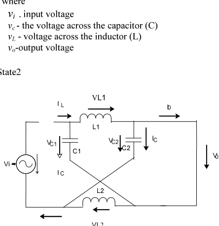
[image:3.595.308.530.236.465.2]State2
Figure 4 Equivalent circuit of state 2 (S1 is off and S2 is on)
The equivalent circuit of the state 2 is shown in Figure 4. In this state S1, is turned off and S2 is turned on. During this state, the Z source network capacitors are being discharged while the inductors are being charged by capacitors and store energy. The interval of this state is DT. So,
L C
v
v
=
0
=
Ov
The average voltage of the inductors over one switching period is zero and is given by
(
)(
)
[
+
−
1
−
]
=
0
=
∫
V
DT
V
V
D
T
dt
V
C i C
L (3)
We get
VC1 VC2
L1
C1 C2
L2 Vi
IL I0
IC
IC
V0
VL1
VL2
V L2
VC1 V C2 LOAD
L1
C1 C2
L2 Vi
I L I0
I L I C
V L1
D
D
V
V
i C
2
1
1
−
−
=
(4)Because the dead time is ignored, assuming the filter inductor and Z source network inductors are very small, there is no line frequency voltage drop across the inductor, the voltage across the load (V0) should be equal to the voltage across
the capacitor of the Z source network (Vc)
i
O
V
D
D
V
2
1
1
−
−
=
(5)From this equation, clearly, the output voltage can be bucked or boosted by controlling the duty ratio, D.
5. CONTROL SCHEME
The switching pulses are generated by using sinusoidal PWM techniques. A high-frequency triangular carrier signal Vc is compared
with a sinusoidal reference signal Vr. The
intersection of Vc and Vr waves are used to
determine the switching instants and commutation of the modulated pulse. The amplitude ratio of the modulating sinusoidal signal to that of triangular carrier signal is known as the modulation index. By varying the modulation index the amplitude of the applied output voltage can be controlled. The PWM pulse is directly fed to bidirectional switch S2 and the complement of the signal is fed to switch S1.
6. SIMULATION RESULTS
In order to verify the performance of the Z source AC-AC converter based DVR for the mitigation of voltage sag and swell, the proposed system is simulated using Matlab/Simulink. The simulation parameters are selected as (i) Input Voltage 110 V (ii) Z source network:L1=L2=1mH
and C1=C2=3.3.μF (iii)Load Resistance R= 50 ohm
(iv)Filter parameters : Lf= 4mH and Cf=10 μF and
(v)Switching frequency : 20 KHz. Here two different cases are considered. In case 1 voltage sag is simulated where as in case 2 voltages swell is simulated.
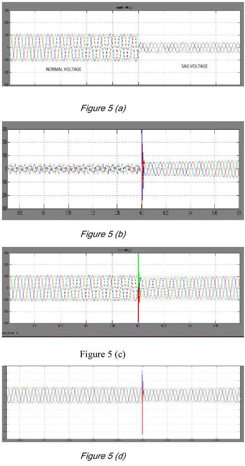
6.1 Voltage Sag
Initially, the system was subjected to three-phase balanced sag of 36% magnitude from t=0.3 msec to t=0.5 msec as shown in Figure 5(a).Figure 5(b) shows the voltage injected by DVR, Figure 5(c) shows the compensated load voltage and Figure 5(d) shows the corresponding load current. The response time of the proposed DVR is less than one cycle.
Figure 5 (a)
Figure 5 (b)
Figure 5 (c)
Figure 5 (d)
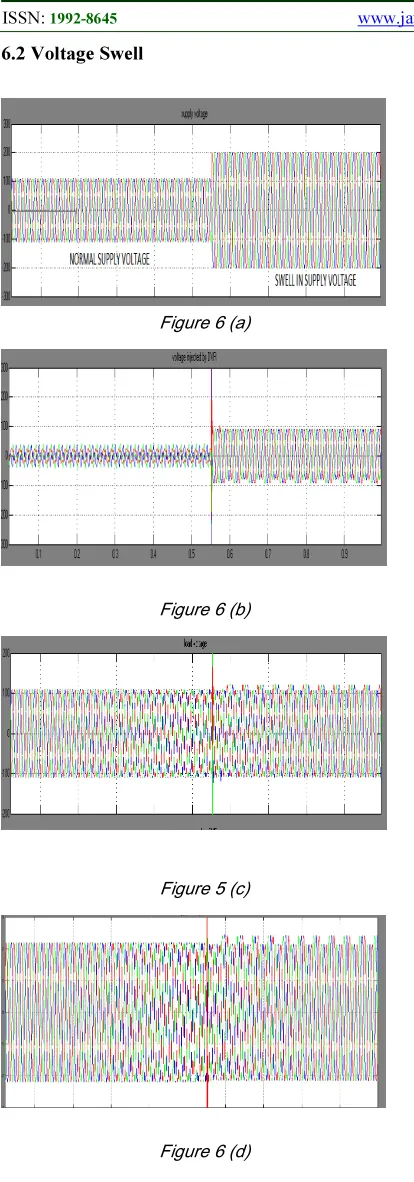
[image:4.595.303.550.253.722.2]6.2 Voltage Swell
Figure 6 (a)
Figure 6 (b)
Figure 5 (c)
Figure 6 (d)
Figure 6 (a) Source voltage (b) Voltage Injected by DVR (c) Compensated load voltage (d) Load current
The supply voltage swell is generated as shown in Figure 6(a).The magnitude of supply voltage is increased about 180 % of nominal voltage at t= 0.55 m sec . The voltage injected by DVR is shown in Figure (b) and the compensated voltage is shown in Figure 6(c) and Figure 6(d) shows the corresponding load current. From the waveform, it is clear that the DVR compensates the voltage swell by injecting appropriated negative voltage magnitude.
7. CONCLUSION
In this paper, DVR utilizing Z source AC-AC converter has been proposed for the mitigation of voltage sag/swell. The three phase Z source AC-AC converter has been used to perform the direct AC/AC conversion. Hence this system does not require any battery energy storage devices. The bidirectional switches have been used which is able to block the voltage and conduct current in both directions. The proposed system provides output voltage which can be bucked/boosted and in-phase /out of phase with the supply voltage. Sinusoidal pulse width modulation technique has been used to generate the gate pulse for the bidirectional switches. The DVR is simulated using Matlab/simulink. The simulation results show that the proposed DVR compensates voltage sag/ voltage swell quickly and provides efficient voltage regulation.
REFRENCES:
[1] Hingorani, N.G, “Introducing custom power”,IEEE Spectrum,1995,1,pp.41-48 [2] C. Fitzer,M.Bar P.Green, “ Voltage Sag
Detection Technique for a Dynamic Voltage Restorer”,IEEE Transactions on Industry application, Issue 1, Vol.40,pp.203-212,Feb.2004.
[3] S.Choi,J.D.Liand D.Mahinda Vilathgamuwa, “ A Generalized Voltage Compensation Strategy for Mitigating the Impacts of Voltage Sags/Swells,” IEEE Transactions on power delivery, vol.20,no.3,July 2005
[4] Takushi Jimichi, Hideaki Fujita and Hirofumi Akagi, “ Design and experimentation of a dynamic voltage restorer capable of significantly reducing an energy –storage element,” IEEE Trans.on Industry Application,vol44,no.3,pp.817-825,May/June 2008
[5] H.P.Tiwari,S.K.Gupta, “ Dynamic Voltage Restorer Based on Load condition”,
[image:5.595.87.294.106.697.2]Management and Technology , Vol.1(1), April 2010,pp. 75-81
[6] Peng FZ.Z-source inverter.IEEE Trans.Industry applications 2004;39:504-510.
[7] Loh PC, Vilathgamuwa DM, Lai YS , Ghua GT, Li Y. Pulse width modulation of z source inverters.J IEEE Trans Power Electron 2005 ; 20 (6) : 1346-55
[8]P.C.Loh,D.M.Vilathgamuwa,Y.S.Lai,G.T.Chua, and Y.Li, “Voltage sag compensation with Z-source inverter based dynamic voltage restorer”,in Industrial application,volume-5 October 2006nes,
[9] Fang XP,Qian ZM, Peng FZ . singlephase z -source PWM ac-ac converters.J IEEE Power Electron Lett 2005;3(4):121-4
[10] Tang Y,Xie S Zhang C.Z-source ac-ac converters solving commutation problem. J IEEE Trans Power Electron 2007 ;22(6):2146-54.
[11] F.Zhang,X.P.Fang,F.Z.Peng and Z.M. Qian, “ A new three-phase ac-ac Z source converter”,in Proc.IEEE Applied Power Electronics Conf.,2006,pp.123-126