2019 International Conference on Artificial Intelligence, Control and Automation Engineering (AICAE 2019) ISBN: 978-1-60595-643-5
Timing Circuit Design Based on Sequential Logic and
Micro-processing Technology
Qing-tian HAN
Naval Aviation University, Yantai, China
Keywords: Sequential logic circuit, Teseter, Circuit design.
Abstract. According to the need of equipment testing, the paper presented the overall scheme of timing circuit and the wiring diagram of hardware circuit, and also designed the indicator circuit, the timing software and the band switch circuit. Then modular design concept and function decomposition method were adopted, and the time sequence step-by-step technology and safety isolation technology were used to solve the difficulty and credibility of acquiring multi-functional components, multi-system modules and complex multi-channel correlated signal interference problem. Finally, the off-line debugging was carried out. The results show that the technology can test the functions and performance indexes of the plug-in board comprehensively and completely, realize the functions of depth setting system debugging, extension testing and fault precise location, and shorten the maintenance and detection time.
Introduction
In order to meet the needs of work, speed up the progress of equipment development, according to the requirements of improving maintenance capacity, we need to make use of rich experience in the development of testing equipment, and accelerate the production of supporting testing equipment, which is of great significance. The relative research was carried out based on the tests. Therefore, aiming at the test requirements, this paper designs the overall scheme of timing circuit, hardware circuit wiring diagram, indicator circuit, timing software and band switch circuit.
Overall Design of Timing Circuit
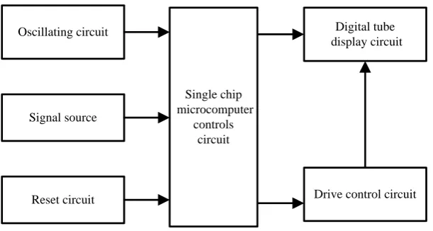
The most important thing in circuit design is to design the overall circuit, including function, index, size, circuit, voltage, input and output, etc. There are four relatively independent loops in the timing circuit: the start loop consisting of start-up 1 and start-up 2, the stop loop consisting of stop 1 and stop 2, the put-in pulse circuit consisting of throw-in pulse and GND (earth), and the display circuit consisting of + 5V power supply and earth. The display circuit consists of a time display circuit and a counting display circuit. So that, the overall block diagram is shown in Figure 1.
Oscillating circuit
Signal source
Single chip microcomputer
controls circuit
From components
Reset circuit
Digital tube display circuit
[image:2.595.145.451.88.251.2]Drive control circuit
Figure 1. Schematic block diagram.
The specific working process of the timing circuit: before the input of + 27V pulse, the relays SB3.2 and SB4.2 are disconnected, and the time display circuit and the counting display circuit are displayed at 0. When the input pulse is put in, the relay SB3.2 absorbs, the starting circuit forms a loop and starts to work; while the starting circuit starts to work, the time display circuit starts to time, and the number of counting display circuit increases by 1. When the input pulse is finished, the relay SB4.2 is sucked, the SB3.2 is disconnected, the circuit is stopped to form a loop, and the time display circuit stops timing, and the number of the counting display circuit does not change. When the next pulse is input again, repeat the above process.
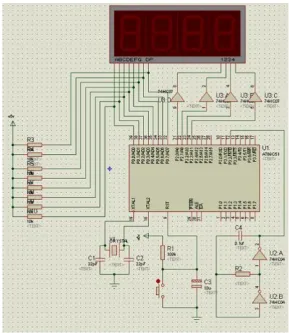
Hardware Design
Figure 2. Hardware circuit wiring diagram.
Timing Software Design
The main program flow chart of the timing software is as follows: Step 1: Initialization.
Step 2: Convert measurements to decimal numbers.
Step 3: Break down the number of uncompressed BCD modes. Step 4: Call the display subroutine.
Step 5: Return to Step 2.
Indicator Circuit Design
Because there are a large number of indicators in the circuit and the circuit of the indicator is identical, only 28, 29 and 30 indicators are intercepted for analysis. The circuit design of the indicator is shown in Figure 3.
Figure 3. Indicator circuit design.
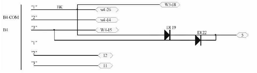
Band Switching Circuit Design
The design of the band switch circuit is shown in Figure 4. Switching circuit design needs to clarify the voltage and current requirements, as well as the relationship between input and output signals. At the same time, we should consider the manual operation habits. Band switch is a conversion switch, which contains two layers of synchronous conversion. When the switch is switched to a certain position on the first layer, the second layer is also switched to the same position. When B4 reaches the "1" position, connect pins S3-18 and S4-26. S3-18 is a + 27V signal generated by the button generated by the tester and input to the placement device. S4-26 receives the + 27V signal transmitted by S3-18. When B4 reaches the "2" position, the pin S4-14 receives the + 27V manual preparation signal provided by the tester. When B4 reaches the "3" position, the pin S4-15 receives the + 27V automatic preparation signal provided by the tester.
Figure 4. Switching circuit design.
The test connection diagram of the tester is shown in Figure 10. Input the right-angle pulse and time instruction information respectively, the tester can display the corresponding output voltage and current values according to the requirements, and the values and errors meet the test and test requirements.
Panel Design
[image:4.595.78.516.413.538.2]technology and high-speed signal processing method. Combined with function testing and fault location, real-time and accurate display of multi-channel time pulse signal is realized, and semi-automatic test and semi-automatic result are achieved. The off-line test and verification technology is used to realize the full function and performance test of the control system. It can realize the functions of system joint debugging, separate test of extension, fault diagnosis isolation and so on. The off-line debugging and verification technology is used to complete the functions and performance indicators of the test plug-in board, realize the functions of depth setting system debugging, extension testing and fault accurate location, and shorten the maintenance and inspection time.
References
[1] Zhang Baozhen, Wang Ping, Yu Xiaowei, et al. Developments of comprehensive testing and diagnosis technology. International Journal of Aviation, 2009 (1), pp. 78-79.
[2] Zhang Baozhen. Trend analysis of foreign military test and test technology development. Computer measurement and control. 2009, 17 (1), pp. 1-5.
[3] Wu Jianqiu, Liang Xiaoyang, Yang Hao. Aeronautical test system based on PC/104 bus. Electronic technology, 2002 (5), pp. 10-12.
[4] Zhang Qi, Hou Jialin, Yan Yinfa, et al. Research on circuit board fault detection and diagnosis system based on virtual instrument. Journal of Electronic Measurement and Instrument, 2011, 25 (2), pp. 140-143.
[5] Chen Zungen. Design of automatic detection system for aviation anti-submarine torpedo. Computer measurement and control, 2002 (9), pp. 1-3.
[6] Wu Quan. Design of high-speed data acquisition system. Electronic measurement technology, 2006, 29 (3), pp. 87-89.