INTRODUCTION TO
NANOTECHNOLOGY
Charles P. Poole, Jr.
Frank J. Owens
@z+::iCIENcE
Published by John Wiley & Sons, Inc., Hoboken, New Jersey. Published simultaneously in Canada.
No part of this publication may be reproduced, stored in a retrieval system, or transmitted in any form or by any means, electronic, mechanical, photocopying, recording, scanning, or otherwise, except as permitted under Section 107 or 108 of the 1976 United States Copyright Act, without either the prior written permission of the Publisher, or authorization through payment of the appropriate per-copy fee to the Copyright Clearance Center, Inc.. 222 Rosewood Drive, Danvers, MA 01923. 978-750-8400, fax 978-750-4470, or on the web at www.copyright.com. Requests to the Publisher for permission should be addressed to the Permissions Department, John Wiley & Sons, Inc., 11 1 River Street, Hoboken, NJ 07030, (201) 748-601 1, fax (201) 748-6008, e-mail: [email protected].
Limit of Liability/Disclaimer of Warranty: While the publisher and author have used their best efforts in preparing this book, they make no representations or warranties with respect to the accuracy or completeness of the contents of this book and specifically disclaim any implied warranties of merchantability or fitness for a particular purpose. No warranty may be created or extended by sales representatives or written sales materials. The advice and strategies contained herein may not be suitable for your situation. You should consult with a professional where appropriate. Neither the publisher nor
author shall be liable for any loss of profit or any other commercial damages, including but not limited to special, incidental, consequential, or other damages.
For general information on our other products and services please contact our Customer Care Department within the US. at 877-762-2974, outside the U S . at 3 17-572-3993 or fax 317-572-4002.
Wiley also publishes its books in a variety of electronic formats. Some content that appears in print, however, may not be available in electronic format.
Library of Congress Cataloging-in-Publication Data:
Poole, Charles P
Introduction to nanotechnology/Charles P Poole, Jr., Frank J. Owens. “A Wiley-Interscience publication.”
Includes bibliographical references and index.
1. Nanotechnology. I. Owens, Frank J. 11. Title p.cm.
ISBN 0-471 -07935-9 (cloth)
T174.7. P66 2003
6 2 0 . 5 4 ~ 2 1 2002191031
Printed in the United States of America
CONTENTS
Preface xi
1 Introduction 1
2 Introduction to Physics of the Solid State 8
2.1 Structure 8 2.1.1
2.1.2 Crystal Structures 9
2.1.3 Face-Centered Cubic Nanoparticles 12
2.1.4 Tetrahedrally Bonded Semiconductor Structures 15 2.1.5 Lattice Vibrations 18
Size Dependence of Properties 8
2.2 Energy Bands 20 2.2.1
2.2.2 Reciprocal Space 22 2.2.3
2.2.4 Effective Masses 28 2.2.5 Fermi Surfaces 29
Insulators, Semiconductors, and Conductors 20
Energy Bonds and Gaps of Semiconductors 23
2.3 Localized Particles 30 2.3.1
2.3.2 Mobility 31 2.3.3 Excitons 32
Donors, Acceptors, and Deep Traps 30
3 Methods of Measuring Properties
3.1 Introduction 35
3.2 Structure 36
3.2.1 Atomic Structures 36 3.2.2 Crystallography 37
35
3.2.3 Particle Size Determination 42 3.2.4 Surface Structure 45
3.3 Microscopy 46
3.3.1 Transmission Electron Microscopy 46 3.3.2 Field Ion Microscopy 51
3.3.3 Scanning Microscopy 51
3.4 Spectroscopy 58 3.4.1
3.4.2
3.4.3 Magnetic Resonance 68
Infrared and Raman Spectroscopy 58 Photoemission and X-Ray Spectroscopy 62
4 Properties of Individual Nanoparticles
4.1 Introduction 72
4.2 Metal Nanoclusters 74 4.2.1 Magic Numbers 74 4.2.2
4.2.3 Geometric Structure 78 4.2.4 Electronic Structure 81 4.2.5 Reactivity 83
4.2.6 Fluctuations 86 4.2.7 Magnetic Clusters 86 4.2.8 Bulk to Nanotransition 88
4.3 Semiconducting Nanoparticles 90 4.3.1 Optical Properties 90 4.3.2 Photofkagmentation 92 4.3.3 Coulombic Explosion 93
4.4 Rare Gas and Molecular Clusters 94 4.4.1 Inert-Gas Clusters 94 4.4.2 Superfluid Clusters 95 4.4.3 Molecular Clusters 96
Theoretical Modeling of Nanoparticles 75
4.5 Methods of Synthesis 97 4.5.1 RF Plasma 97 4.5.2 Chemical Methods 98 4.5.3 Thermolysis 99
4.5.4 Pulsed Laser Methods 100
4.6 Conclusion 101
5 Carbon Nanostructures
5.1 Introduction 103
72
CONTENTS Vii 5.2 Carbon Molecules 103
5.2.1 Nature of the Carbon Bond 103 5.2.2 New Carbon Structures 105
5.3 Carbon Clusters 106
5.3.1 Small Carbon Clusters 106 5.3.2 Discovery of c60 107 5.3.3
5.3.4 Alkali-Doped c 6 0 110 5.3.5 Superconductivity in c60 112 5.3.6
5.3.7 Other Buckyballs 113
Structure of c 6 0 and Its Crystal 110
Larger and Smaller Fullerenes 113
5.4 Carbon Nanotubes 114 5.4.1 Fabrication 114 5.4.2 Structure 117
5.4.3 Electrical Properties 11 8 5.4.4 Vibrational Properties 122 5.4.5 Mechanical Properties 123
5.5 Applications of Carbon Nanotubes 125 5.5.1
5.5.2 Computers 126 5.5.3 Fuel Cells 127 5.5.4 Chemical Sensors 128 5.5.5 Catalysis 129
5.5.6 Mechanical Reinforcement 130 Field Emission and Shielding 125
6 Bulk Nanostructured Materials
6.1 Solid Disordered Nanostructures 133 6.1.1 Methods of Synthesis 133
6.1.2 Failure Mechanisms of Conventional Grain-Sized Materials 137
6.1.3 Mechanical Properties 139 6.1.4 Nanostructured Multilayers 141 6.1.5 Electrical Properties 142 6.1.6 Other Properties 147 6.1.7
6.1.8 Porous Silicon 150
Metal Nanocluster Composite Glasses 148
6.2 Nanostructured Crystals 153 6.2.1 Natural Nanocrystals 153 6.2.2
6.2.3 6.2.4
Computational Prediction of Cluster Lattices 153 Arrays of Nanoparticles in Zeolites 154
Crystals of Metal Nanoparticles 157
6.2.5 Nanoparticle Lattices in Colloidal Suspensions 158 6.2.6 Photonic Crystals 159
7 Nanostructured Ferromagnetism
7.1 Basics of Ferromagnetism 165
7.2
7.3 Dynamics of Nanomagnets 172
7.4 Nanopore Containment of Magnetic Particles 176
7.5 Nanocarbon Ferromagnets 177
7.6
7.7 Ferrofluids 186
Effect of Bulk Nanostructuring of Magnetic Properties 170
Giant and Colossal Magnetoresistance 18 1
8 Optical and Vibrational Spectroscopy
8.1 Introduction 194
8.2 Infrared Frequency Range 196 8.2.1
8.2.2 Infrared Surface Spectroscopy 198 8.2.3 Raman Spectroscopy 203
8.2.4 Brillouin Spectroscopy 210
Spectroscopy of Semiconductors; Excitons 196
8.3 Luminescence 213
8.3.1 Photoluminescence 213 8.3.2 Surface States 215 8.3.3 Thermoluminescence 221
Nanostructures in Zeolite Cages 222 8.4
9 Quantum Wells, Wires, and Dots
9.1 Introduction 226
9.2
9.3
Preparation of Quantum Nanostructures 227
Size and Dimensionality Effects 231 9.3.1 Size Effects 231
9.3.2 9.3.3
9.3.4 Potential Wells 236 9.3.5 Partial Confinement 241 9.3.6
Conduction Electrons and Dimensionality 233 Fermi Gas and Density of States 234
Properties Dependent on Density of States 242
165
194
CONTENTS iX 9.4 Excitons 244
9.5 Single-Electron Tunneling 245
9.6 Applications 248
9.6.1 Infrared Detectors 248 9.6.2 Quantum Dot Lasers 251
9.7 Superconductivity 253
10 Self-Assembly and Catalysis
10.1 Self-Assembly 257
10.1.1 Process of Self-Assembly 257 10.1.2 Semiconductor Islands 258 10.1.3 Monolayers 260
10.2 Catalysis 264
10.2.1 Nature of Catalysis 264 10.2.2
10.2.3 Porous Materials 268 10.2.4 Pillared Clays 273 10.2.5 Colloids 277
Surface Area of Nanoparticles 264
11 Organic Compounds and Polymers
1 1.1 Introduction 28 1
1 1.2 Forming and Characterizing Polymers 283 1 1.2.1 Polymerization 283
11.2.2 Sizes of Polymers 284
11.3 Nanocrystals 285 1 1.3.1
11.3.2 Polydiacetylene Types 289 Condensed Ring Types 285
11.4 Polymers 292
1 1.4.1 Conductive Polymers 292 1 1.4.2 Block Copolymers 293
11.5 Supramolecular Structures 295
1 1.5.1 Transition-Metal-Mediated Types 295 1 1.5.2 Dendritic Molecules 296
11.5.3 Supramolecular Dendrimers 302 11.5.4 Micelles 305
257
12 Biological Materials
12.1 Introduction 3 10
12.2 Biological Building Blocks 3 1 1 12.2.1
12.2.2
Sizes of Building Blocks and Nanostructures 3 11 Polypeptide Nanowire and Protein Nanoparticle 3 14
12.3 Nucleic Acids 3 16
12.3.1 DNA Double Nanowire 316
12.3.2 Genetic Code and Protein Synthesis 322
12.4 Biological Nanostructures 324 12.4.1 Examples of Proteins 324 12.4.2 Micelles and Vesicles 326 12.4.3 Multilayer Films 329
13 Nanomachines and Nanodevices
13.1 Microelectromechanical Systems (MEMSs) 332
13.2 Nanoelectromechanical Systems (NEMSs) 335 13.2.1 Fabrication 335
13.2.2 Nanodevices and Nanomachines 339
Molecular and Supramolecular Switches 345 13.3
A Formulas for Dimensionality
A. 1 Introduction 357 A.2 Delocalization 357
A.3 Partial Confinement 358
B Tabulations of Semiconducting Material Properties
Index
31 0
332
357
361
PREFACE
In recent years nanotechnology has become one of the most important and exciting forefront fields in Physics, Chemistry, Engineering and Biology. It shows great promise for providing us in the near future with many breakthroughs that will change the direction of technological advances in a wide range of applications. To facilitate the timely widespread utilization of this new technology it is important to have available an overall summary and commentary on this subject which is sufficiently detailed to provide a broad coverage and insight into the area, and at the same time is sufficiently readable and thorough so that it can reach a wide audience of those who have a need to know the nature and prospects for the field. The present book hopes to achieve these two aims.
The current widespread interest in nanotechnology dates back to the years 1996 to 1998 when a panel under the auspices of the World Technology Evaluation Center (WTEC), funded by the National Science Foundation and other federal agencies, undertook a world-wide study of research and development in the area of nano- technology, with the purpose of assessing its potential for technological innovation. Nanotechnology is based on the recognition that particles less than the size of 100 nanometers (a nanometer is a billionth of a meter) impart to nanostructures built from them new properties and behavior. This happens because particles which are smaller than the characteristic lengths associated with particular phenomena often display new chemistry and physics, leading to new behavior which depends on the size. So, for example, the electronic structure, conductivity, reactivity, melting temperature, and mechanical properties have all been observed to change when particles become smaller than a critical size. The dependence of the behavior on the particle sizes can allow one to engineer their properties. The WTEC study concluded that this technology has enormous potential to contribute to significant advances over a wide and diverse range of technological areas ranging from producing stronger and lighter materials, to shortening the delivery time of nano structured pharmaceuticals to the body’s circulatory system, increasing the storage capacity of magnetic tapes, and providing faster switches for computers. Recommendations made by this and subsequent panels have led to the appropriation of very high levels of finding in recent years. The research area of nanotechnology is interdisciplinary,
covering a wide variety of subjects ranging from the chemistry of the catalysis of nanoparticles, to the physics of the quantum dot laser. As a result researchers in any one particular area need to reach beyond their expertise in order to appreciate the broader implications of nanotechnology, and learn how to contribute to this exciting new field. Technical managers, evaluators, and those who must make funding decisions will need to understand a wide variety of disciplines. Although this book was originally intended to be an introduction to nanotechnology, due to the nature of the field it has developed into an introduction to selected topics in nanotechnology, which are thought to be representative of the overall field. Because of the rapid pace of development of the subject, and its interdisciplinary nature, a truly comprehensive coverage does not seem feasible. The topics presented here were chosen based on the maturity of understanding of the subjects, their potential for applications, or the number of already existing applications. Many of the chapters discuss present and future possibilities. General references are included for those who wish to pursue fiuther some of the areas in which this technology is moving ahead.
We have attempted to provide an introduction to the subject of nanotechnology written at a level such that researchers in different areas can obtain an appreciation of developments outside their present areas of expertise, and so that technical administrators and managers can obtain an overview of the subject. It is possible that such a book could be used as a text for a graduate course on nanotechnology. Many of the chapters contain introductions to the basic physical and chemical principles of the subject area under discussion, hence the various chapters are self contained, and may be read independently of each other. Thus Chapter 2 begins with a brief overview of the properties of bulk materials that need to be understood if one is to appreciate how, and why, changes occur in these materials when their sizes approach a billionth of a meter. An important impetus that caused nanotechnology to advance so rapidly has been the development of instrumentation such as the scanning tunneling microscope that allows the visualization of the surfaces of nanometer sized materials. Hence Chapter 3 presents descriptions of important instrumentation systems, and provides illustrations of measurements on nano materials. The remaining chapters cover various aspects of the field.
INTRODUCTION
The prefix nano in the word nanotechnology means a billionth (1 x lop9). Nanotechnology deals with various structures of matter having dimensions of the order of a billionth of a meter. While the word nanotechnology is relatively new, the existence of functional devices and structures of nanometer dimensions is not new, and in fact such structures have existed on Earth as long as life itself. The abalone, a mollusk, constructs very strong shells having iridescent inner surfaces by organizing calcium carbonate into strong nanostructured bricks held together by a glue made of a carbohydrate-protein mix. Cracks initiated on the outside are unable to move through the shell because of the nanostructured bricks. The shells represent a natural demonstration that a structure fabricated from nanoparticles can be much stronger. We will discuss how and why nanostructuring leads to stronger materials in Chapter 6.
It is not clear when humans first began to take advantage of nanosized materials. It is known that in the fourth-century A.D. Roman glassmakers were fabricating glasses containing nanosized metals. An artifact from this period called the Lycurgus cup resides in the British Museum in London. The cup, which depicts the death of King Lycurgus, is made from soda lime glass containing sliver and gold nanopar- ticles. The color of the cup changes from green to a deep red when a light source is placed inside it. The great varieties of beautiful colors of the windows of medieval cathedrals are due to the presence of metal nanoparticles in the glass.
Introduction to Nunotechnology, by Charles P. Poole Jr. and Frank J. Owens. ISBN 0471-07935-9. Copyright 0 2003 John Wiley & Sons, Inc.
The potential importance of clusters was recognized by the Irish-born chemist Robert Boyle in his Sceptical Chyrnist published in 1661. In it Boyle criticizes Aristotle’s belief that matter is composed of four elements: earth, fire, water, and air. Instead, he suggests that tiny particles of matter combine in various ways to form what he calls corpuscles. He refers to “minute masses or clusters that were not easily dissipable into such particles that composed them.”
Photography is an advanced and mature technology, developed in the eighteenth and nineteenth centuries, which depends on production of silver nanoparticles sen- sitive to light. Photographic film is an emulsion, a thin layer of gelatin containing silver halides, such as silver bromide, and a base of transparent cellulose acetate. The light decomposes the silver halides, producing nanoparticles of silver, which are the pixels of the image. In the late eighteenth century the British scientists Thomas Wedgewood and Sir Humprey Davy were able to produce images using silver nitrate and chloride, but their images were not permanent. A number of French and British researchers worked on the problem in the nineteenth century. Such names as Daguerre, Niecpce, Talbot, Archer, and Kennet were involved. Interestingly James Clark Maxwell, whose major contributions were to electromagnetic theory, produced the first color photograph in 1861. Around 1883 the American inventor George Eastman, who would later found the Kodak Corporation, produced a film consisting of a long paper strip coated with an emulsion containing silver halides. He later developed this into a flexible film that could be rolled, which made photography accessible to many. So technology based on nanosized materials is really not that new.
In 1857 Michael Faraday published a paper in the Philosophical Transactions of the Royal SocieQ, which attempted to explain how metal particles affect the color of church windows. Gustav Mie was the first to provide an explanation of the dependence of the color of the glasses on metal size and kind. His paper was published in the German Journal Annalen der Physik (Leipzig) in 1908.
INTRODUCTION 3 he recognized the existence of nanostructures in biological systems. Many of Feynman’s speculations have become reality. However, his thinking did not resonate with scientists at the time. Perhaps because of his reputation for wit, the reaction of many in the audience could best be described by the title of his later book Surely You i-e Joking, A4r Feynman. Of course, the lecture is now legendary among present- day nanotechnology researchers, but as one scientist has commented, “it was so visionary that it did not connect with people until the technology caught up with it.” There were other visionaries. Ralph Landauer, a theoretical physicist working for IBM in 1957, had ideas on nanoscale electronics and realized the importance that quantum-mechanical effects would play in such devices.
Although Feynman presented his visionary lecture in 1960, there was experi- mental activity in the 1950s and 1960s on small metal particles. It was not called nanotechnology at that time, and there was not much of it. Uhlir reported the first observation of porous silicon in 1956, but it was not until 1990 when room- temperature fluorescence was observed in this material that interest grew. The properties of porous silicon are discussed in Chapter 6. Other work in this era involved making alkali metal nanoparticles by vaporizing sodium or potassium metal and then condensing them on cooler materials called substrates. Magnetic fluids called ferrofluids were developed in the 1960s. They consist of nanosized magnetic particles dispersed in liquids. The particles were made by ballmilling in the presence of a surface-active agent (surfactant) and liquid carrier. They have a number of interesting properties and applications, which are discussed in Chapter 7. Another area of activity in the 1960s involved electron paramagnetic resonance (EPR) of conduction electrons in metal particles of nanodimensions referred to as colloids in those days. The particles were produced by thermal decomposition and irradiation of solids having positive metal ions, and negative molecular ions such as sodium and potassium azide. In fact, decomposing these kinds of solids by heat is one way to make nanometal particles, and we discuss this subject in Chapter 4. Structural features of metal nanoparticles such as the existence of magic numbers were revealed in the 1970s using mass spectroscopic studies of sodium metal beams. Herman and co-workers measured the ionization potential of sodium clusters in 1978 and observed that it depended on the size of the cluster, which led to the development of the jellium model of clusters discussed in Chapter 4.
Groups at Bell Laboratories and IBM fabricated the first two-dimensional quantum wells in the early 1970s. They were made by thin-film (epitaxial) growth techniques that build a semiconductor layer one atom at a time. The work was the beginning of the development of the zero-dimensional quantum dot, which is now one of the more mature nanotechnologies with commercial applications. The quantum dot and its applications are discussed in Chapter 9.
method was used to synthesize the fullerene (c6,). In 1982, two Russian scientists, Ekimov and Omushchenko, reported the first observation of quantum confinement, which is discussed in Chapter 9. The scanning tunneling microscope was developed during this decade by G . K. Binnig and H. Roher of the IBM Research Laboratory in Zurich, and they were awarded the Nobel Prize in 1986 for this. The invention of the scanning tunneling microscope (STM) and the atomic force microscope (AFM), which are described in Chapter 3, provided new important tools for viewing, characterizing, and atomic manipulation of nanostructures. In 1987, B. J. van Wees and H. van Houten of the Netherlands observed steps in the current-voltage curves of small point contacts. Similar steps were observed by D. Wharam and M. Pepper of Cambridge University. This represented the first observation of the quantization of conductance. At the same time T. A. Fulton and G . J. Dolan of Bell Laboratories made a single-electron transistor and observed the Coulomb blockade, which is explained in Chapter 9. This period was marked by development of methods of fabrication such as electron-beam lithography, which are capable of producing 10-nm structures. Also in this decade layered alternating metal magnetic and nonmagnetic materials, which displayed the fascinating property of giant magne- toresistance, were fabricated. The layers were a nanometer thick, and the materials have an important application in magnetic storage devices in computers. This subject is discussed in Chapter 7.
Although the concept of photonic crystals was theoretically formulated in the late 1980s, the first three-dimensional periodic photonic crystal possessing a complete bandgap was fabricated by Yablonovitch in 199 1. Photonic crystals are discussed in Chapter 6. In the 1990s, Iijima made carbon nanotubes, and superconductivity and ferromagnetism were found in c60structures. Efforts also began to make molecular switches and measure the electrical conductivity of molecules. A field-effect transistor based on carbon nanotubes was demonstrated. All of these subjects are discussed in this book. The study of self-assembly of molecules on metal surfaces intensified. Self-assembly refers to the spontaneous bonding of molecules to metal surfaces, forming an organized array of molecules on the surface. Self-assembly of thiol and disulfide compounds on gold has been most widely studied, and the work is presented in Chapter 10.
In 1996, a number of government agencies led by the National Science Foun- dation commissioned a study to assess the current worldwide status of trends, research, and development in nanoscience and nanotechnology. The detailed recommendations led to a commitment by the government to provide major funding and establish a national nanotechnology initiative. Figure 1.1 shows the growth of U.S. government funding for nanotechnology and the projected increase due to the national nanotechnology initiative. Two general findings emerged from the study.
INTRODUCTION 5 1000
(I)
a 900 I
7997 1998 1999 2000 2001 2002 GOVERNMENT FISCAL YEAR
1000
a 900
6
700f
600 0 500(I) 400
300
(I)
4
8002
200g
1000
1997 1998 1999 2000 2001 2002 GOVERNMENT FISCAL YEAR
Figure 1.1. Funding for nanotechnology research by year. The top tracing indicates spending by
foreign governments; bottom, U.S. government spending. The dashed line represents proposed spending for 2002. (From U.S. Senate Briefing on nanotechnology, May 24, 2001 and National Science Foundation.)
characterized by a length called the scattering length. This length is the average distance an electron travels before being deflected. The fundamental physics and chemistry changes when the dimensions of a solid become comparable to one or more of these characteristic lengths, many of which are in the nanometer range. One of the most important examples of this is what happens when the size of a semiconducting material is in the order of the wavelength of the electrons or holes that carry current. As we discuss in Chapter 9, the electronic structure of the system completely changes. This is the basis of the quantum dot, which is a relatively mature application of nanotechnology resulting in the quantum-dot laser presently used to read compact disks (CDs). However, as we shall see in Chapter 9, the electron structure is strongly influenced by the number of dimensions that are nanosized.
If only one length of a three-dimensional nanostructure is of a nanodimension, the structure is known as a quantum well, and the electronic structure is quite different from the arrangement where two sides are of nanometer length, constituting what is referred to as a quantum wire. A quantum dot has all three dimensions in the nanorange. Chapter 9 discusses in detail the effect of dimension on the electronic properties of nanostructures. The changes in electronic properties with size result in major changes in the optical properties of nanosized materials, which is discussed in Chapter 8, along with the effects of reduced size on the vibrational properties of materials.
2
INTRODUCTION TO
PHYSICS
OF
THE
SOLID STATE
In this book we will be discussing various types of nanostructures. The materials used to form these structures generally have bulk properties that become modified when their sizes are reduced to the nanorange, and the present chapter presents background material on bulk properties of this type. Much of what is discussed here can be found in a standard text on solid-state physics [e.g., Burns (1985); Kittel (1996); see also Yu and Cardona (2001)].
2.1. STRUCTURE
2.1 .l. Size Dependence of Properties
Many properties of solids depend on the size range over which they are measured. Microscopic details become averaged when investigating bulk materials. At the macro- or large-scale range ordinarily studied in traditional fields of physics such as mechanics, electricity and magnetism, and optics, the sizes of the objects under study range from millimeters to kilometers. The properties that we associate with these materials are averaged properties, such as the density and elastic moduli in
2.1. STRUCTURE 9
mechanics, the resistivity and magnetization in electricity and magnetism, and the dielectric constant in optics. When measurements are made in the micrometer or nanometer range, many properties of materials change, such as mechanical, ferroelectric, and ferromagnetic properties. The aim of the present book is to examine characteristics of solids at the next lower level of size, namely, the nanoscale level, perhaps from 1 to l00nm. Below this there is the atomic scale near 0.1 nm, followed by the nuclear scale near a femtometer m). In order to understand properties at the nanoscale level it is necessary to know something about the corresponding properties at the macroscopic and mesoscopic levels, and the present chapter aims to provide some of this background.
Many important nanostmctures are composed of the group IV elements Si or Ge, type 111-V semiconducting compounds such as GaAs, or type 11-VI semiconduct- ing materials such as CdS, so these semiconductor materials will be used to illustrate some of the bulk properties that become modified with incorporation into nano- structures. The Roman numerals IV, 111, V, and so on, refer to columns of the periodic table. Appendix B provides tabulations of various properties of these semiconductors.
2.1.2. Crystal Structures
Most solids are crystalline with their atoms arranged in a regular manner. They have what is called long-range order because the regularity can extend throughout the crystal. In contrast to this, amorphous materials such as glass and wax lack long- range order, but they have what is called short-range order so the local environment of each atom is similar to that of other equivalent atoms, but this regularity does not persist over appreciable distances. Liquids also have short-range order, but lack long-range order. Gases lack both long-range and short-range order.
Figure 2.1 shows the five regular arrangements of lattice points that can occur in two dimensions: the square (a), primitive rectangular (b), centered rectangular (c), hexagonal (d), and oblique (e) types. These arrangements are called Bravais lattices. The general or oblique Bravais lattice has two unequal lattice constants a
#
b and an arbitrary angle 8 between them. For the perpendicular case when 19 = 90°, the lattice becomes the rectangular type. For the special case a = b and 8 = 60°, the lattice is the hexagonal type formed from equilateral triangles. Each lattice has a unit cell, indicated in the figures, which can replicate throughout the plane and generate the lattice.a .
. . . . . .
. . .
. . a
. .
. . .
Figure 2.1. The five Bravais lattices that occur in two dimensions, with the unit cells indicated:
A- B
B-A
A- B
B
-A
A
-B
B-A
A-B
B-A
Figure 2.2. Sketch of a two-dimensional crystal structure based on a primitive rectangular lattice containing two diatomic molecules A-B in each unit cell.
A crystal structure is formed by associating with a lattice a regular arrangement of atoms or molecules. Figure 2.2 presents a two-dimensional crystal structure based on a primitive rectangular lattice containing two diatomic molecules A-B in each unit cell. A single unit cell can generate the overall lattice.
In three dimensions there are three lattice constants, a, b, and c, and three angles:
c( between b and c;
b
between a and c, and y between lattice constants a and b. Thereare 14 Bravais lattices, ranging from the lowest-symmetry triclinic type in which all three lattice constants and all three angles differ from each other (a
#
b#
c andc(
#
b
#
y), to the highest-symmetry cubic case in which all the lattice constants areequal and all the angles are 90" (a = b = c and c( =
b
= y = 90"). There arethree Bravais lattices in the cubic system, namely, a primitive or simple cubic (SC) lattice in which the atoms occupy the eight apices of the cubic unit cell, as shown in Fig. 2.3a, a body-centered cubic (BCC) lattice with lattice points occupied at the apices and in the center of the unit cell, as indicated in Fig. 2.3b, and a face-centered cubic (FCC) Bravais lattice with atoms at the apices and in the centers of the faces, as shown in Fig. 2 . 3 ~ .
In two dimensions the most efficient way to pack identical circles (or spheres) is the equilateral triangle arrangement shown in Fig. 2.4a, corresponding to the hexagonal Bravais lattice of Fig. 2.ld. A second hexagonal layer of spheres can be placed on top of the first to form the most efficient packing of two layers, as shown in Fig. 2.4b. For efficient packing, the third layer can be placed either above
2.1. STRUCTURE 11
T
X
Figure 2.4. Close packing of spheres on a flat surface: (a) for a monolayer; (b) with a second
layer added. The circles of the second layer are drawn smaller for clarity. The location of an octahedral site is indicated by x , and the position of a tetrahedral site is designated by T on panel (b).
the first layer with an atom at the location indicated by T o r in the third possible arrangement with an atom above the position marked by
X
on the figure. In the first case a hexagonal lattice with a hexagonal close-packed (HCP) structure is generated, and in the second case a face-centered cubic lattice results. The former is easy to visualize, but the latter is not so easy to picture.In the three-dimensional case of close-packed spheres there are spaces or sites between the spheres where smaller atoms can reside. The point marked by X on Fig. 2.4b, called an octahedral site, is equidistant from the three spheres 0 below it, and from the three spheres 0 above it. An atom A at this site has the local coordination AO,. The radius aoct, of this octahedral site is
where a is the lattice constant and a. is the radius of the spheres. The number of octahedral sites is equal to the number of spheres. There are also smaller sites, called tetrahedral sites, labeled T in the figure that are equidistant from four nearest- neighbor spheres, one below and three above, corresponding to AO, for the local coordination. This is a smaller site since its radius aT is
octahedral sites and Mg2+ (radius 0.066 nm) located in one-eighth of the tetrahedral sites in a regular manner.
2.1.3. Face-Centered Cubic Nanoparticles
Most metals in the solid state form close-packed lattices; thus Ag, Al, Au, Co, Cu, Pb, Pt, and Rh, as well as the rare gases Ne, Ar, Kr, and Xe, are face-centered cubic (FCC), and Mg, Nd, Os, Re, Ru, Y, and Zn, are hexagonal close-packed (HCP). A number of other metallic atoms crystallize in the not so closely packed body- centered cubic (BCC) lattice, and a few such as Cr, Li, and Sr crystallize in all three structure types, depending on the temperature. An atom in each of the two close- packed lattices has 12 nearest neighbors. Figure 2.5 shows the 12 neighbors that surround an atom (darkened circle) located in the center of a cube for a FCC lattice. Figure 10.18 (of Chapter IO) presents another perspective of the 12 nearest neighbors. These 13 atoms constitute the smallest theoretical nanoparticle for an FCC lattice. Figure 2.6 shows the 14-sided polyhedron, called a dekatessarahedron, that is generated by connecting the atoms with planar faces. Sugano and Koizumi (1998) call this polyhedron a cuboctahedron. The three open circles at the upper right of Fig. 2.6 are the three atoms in the top layer of Fig. 10.18, the six darkened circles plus an atom in the center of the cube of Fig. 2.6 constitute the middle layer of that figure, and the open circle at the lower left of Fig. 2.5 is one of the three obscured atoms in the plane below the cluster pictured in Fig. 10.18. This 14-sided polyhedron has six square faces and eight equilateral triangle faces.
If another layer of 42 atoms is layed down around the 13-atom nanoparticle, one obtains a 55-atom nanoparticle with the same dekatessarahedron shape. Larger
Figure 2.5. Face-centered cubic unit cell showing the 12 nearest-neighbor atoms that surround
2.1. STRUCTURE 13
Figure 2.6. Thirteen-atom nanoparticle set in its FCC unit cell, showing the shape of the 14-
sided polyhedron associated with the nanocluster. The three open circles at the upper right correspond to the atoms of the top layer of the nanoparticle sketched in Fig. 10.8 (of Chapter lo), the six solid circles plus the atom (not pictured) in the center of the cube constitute the middle hexagonal layer of that figure, and the open circle at the lower left corner of the cube is one of the three atoms at the bottom of the cluster of Fig. 10.18.
nanoparticles with the same polyhedral shape are obtained by adding more layers, and the sequence of numbers in the resulting particles, N =
1,13,55,147,309,561,. .., which are listed in Table 2.1, are called structural magic numbers. For n layers the number of atoms N in this FCC nanoparticle is given by the formula
N = i[10n3 - 15n2
+
l l n - 31 (2.3)and the number of atoms on the surface Nsud is
Nsud = 10n2 - 20n + 12 (2.4)
For each value of n, Table 2.1 lists the number of atoms on the surface, as well as the percentage of atoms on the surface. The table also lists the diameter of each nanoparticle, which is given by the expression (2n
-
l)d, where d is the distance between the centers of nearest-neighbor atoms, and d = a / & where a is the lattice constant. If the same procedure is used to construct nanoparticles with the hexagonal close-packed structure that was discussed in the previous section, a slightly different set of structural magic numbers is obtained, namely, 1,13,57,153,321,581,.
. . .Table 2.1. Number of atoms (structural magic numbers) in rare gas or
metallic nanoparticles with face-centered cubic closepacked structuree
Number of FCC Nanoparticle Atoms Shell
Number Diameter Total On Surface YO Surface
1 2 3 4 5 6 I 8 9 I O 11 12 25 50 75 100 Id 3d 5d I d 9d 1 Id 13d 15d 17d 19d 21d 23d 49d 99d 149d 199d 1 13 55 147 309 561 923 1415 2057 2869 3871 5083 4.90 io4 4.04 io5 1.38 x lo6 3.28 x lo6
1 12 42 92 162 252 3 62 492 642 812 1002 1212 5.76 io3 2.40 lo4 5.48 io4 9.80 io4
IO0 92.3 16.4 62.6 52.4 44.9 39.2 34.8 31.2 28.3 25.9 23.8 11.7 5.9 4.0 3.0
"The diameters d in nanometers for some representative FCC atoms are AI 0.286, Ar 0.376, Au 0.288, Cu 0.256, Fe 0.248, Kr 0.400, Pb 0.350, and Pd 0.275.
stabilized form Au55(PPh3)12C16 which has the diameter of -1.4nm, where PPh, is an organic group. Further examples are the magic number nanoparticles Pt3,9( 1, 10-phenantroline),,O,, and Pd561 (1,1O-phenantr0line),,0~,,.
The magic numbers that we have been discussing are called structural magic numbers because they arise from minimum-volume, maximum-density nano- particles that approximate a spherical shape, and have close-packed structures characteristic of a bulk solid. These magic numbers take no account of the electronic structure of the consitituent atoms in the nanoparticle. Sometimes the dominant factor in determining the minimum-energy structure of small nanoparticles is the interactions of the valence electrons of the constituent atoms with an averaged molecular potential, so that the electrons occupy orbital levels associated with this potential. Atomic cluster configurations in which these electrons fill closed shells are especially stable, and constitute electronic magic numbers. Their atomic structures differ from the FCC arrangement, as will be discussed in Sections 4.2.1 and 4.2.2 (of Chapter 4).
When mass spectra were recorded for sodium nanoparticles Na,, it was found that mass peaks corresponding to the first 15 electronic magic numbers N =
2.1. STRUCTURE 15 Sodium Nanoparticle Na, Magic Numbers
Electronic Structural
0 3 6 9 1 2 8 10 I2 14 16
I I I I I I I ; I I I I I I I I ~ I
I I
I:
I
I 1 ; I I
I
5 10 I5 20 2s
n”
Figure 2.7. Dependence of the observed mass spectra lines from Na, nanoparticles on the
cube root N’l3 of the number of atoms N in the cluster. The lines are labeled with the index n of their electronic and structural magic numbers obtained from Martin et al. (1990).
approximately equally spaced, with the spacing between the structural magic numbers about 2.6 times that between the electronic ones. This result provides evidence that small clusters tend to satisfy electronic criteria and large structures tend to be structurally determined.
2.1.4. Tetrahedrally Bonded Semiconductor Structures
The type 111-V and type 11-VI binary semiconducting compounds, such as GaAs and ZnS, respectively, crystallize with one atom situated on a FCC sublattice at the positions 000,
1
0, 0 and 04,
and the other atom on a second FCC sublattice displaced from the first by the amount$$$
along the body diagonal, as shown in Fig. 2.8b. This is called the zinc blende or ZnS structure. It is clear from the figure that each Zn atom (white sphere) is centered in a tetrahedron of S atoms (black spheres), and likewise each S has four similarly situated Zn nearest neighbors. The small half- sized, dashed-line cube delineates one such tetrahedron. The same structure would result if the Zn and S atoms were interchanged.The elements Si and Ge crystallize in this same structure by having the Si (or Ge) atoms occupying all the sites on the two sublattices, so there are eight identical atoms in the unit cell. This atom arrangement, sketched in Fig. 2.8a, is called the diamond structure. Both Si and Ge have a valence of 4, so from bonding con- siderations, it is appropriate for each to be bound to four other atoms in the shape of a regular tetrahedron.
Figure 2.8. Unit cell of the diamond structure (a), which contains only one type of atom, and corresponding unit cell of the zinc blende (sphalerite) structure (b), which contains two atom types. The rods represent the tetrahedral bonds between nearest-neighbor atoms. The small dashed line cube in (b) delineates a tetrahedron. (From G. Burns, Solidstate Physics, Academic Press, Boston, 1985, p.148.)
and as one goes from top to bottom in a particular column. This occurs because of the systematic increase in the size of the atoms in each group with increasing atomic number, as indicated in Table B.2.
There are tiyo simple models for representing these AC binary compound structures. For an ionic model the lattice AnPC"+ consists of a FCC arrangement
Figure 2.9. Packing of larger S atoms and smaller Zn atoms in the zinc blende (ZnS) structure.
2.1. STRUCTURE 17
of the large anions A"- with the small cations C"+ located in the tetrahedral sites of the anion FCC lattice. If the anions touch each other, their radii have the value
a. = a/21/2, where a is the lattice parameter, and the radius aT of the tetrahedral site aT = 0 . 2 2 4 7 ~ ~ is given by Eq. (2.2). This is the case for the very small Ai3+ cation in the AlSb structure. In all other cases the cations in Table B.2 are too large to fit in the tetrahedral site so they push the larger anions further apart, and the latter no longer touch each other, in accordance with Fig. 2.9. In a covalent model for the structure consisting of neutral atoms A and C the atom sizes are comparable, as the data in Table B.2 indicate, and the structure resembles that of Si or Ge. To compare these two models, we note that the distance between atom A at lattice position 0 0 0 and its nearest neighbor C at position is equal to t a u , and in Table B.3 we compare this crystallographically evaluated distance with the sums of radii of ions A"-, C"+ from the ionic model, and with the sums of radii of neutral atoms A and C of the covalent model using the data of Table B.2. We see from the results on Table B.3 that neither model fits the data in all cases, but the neutral atom covalent model is closer to agreement. For comparison purposes we also list corresponding data for several alkali halides and alkaline-earth chalcogenides that crystallize in the cubic rock salt or NaCl structure, and we see that all of these compounds fit the ionic model very well. In these compounds each atom type forms a FCC lattice, with the atoms of one FCC lattice located at octahedral sites of the other lattice. The octahedral site has the radius aoct = 0.4141 la, given by Eq. (2.1), which is larger than the tetrahedral one of Eq. (2.2).
Since the alkali halide and alkaline-earth chalcogenide compounds fit the ionic model so well, it is significant that neither model fits the structures of the semiconductor compounds. The extent to which the semiconductor crystals exhibit ionic or covalent bonding is not clear from crystallographic data. If the wavefunction describing the bonding is written in the form
where the coefficients of the covalent and ionic wavefunction components are normalized
2
acov +ai?,, = 1
then a:ov is the fractional covalency and ai?,, is the fractional ionicity of the bond. A chapter (Poole and Farach 2001) in a book by Karl Boer (2001) tabulates the effective charges e* associated with various 11-VI and 111-V semiconducting compounds, and this effective charge is related to the fractional covalency by the expression
where N = 2 for 11-VI and N = 3 for 111-V compounds. The fractional charges all lie in the range from 0.43 to 0.49 for the compounds under consideration. Using the e* tabulations in the Boer book and Eq. (2.7), we obtain the fractional covalencies of a:ov
-
0.81 for all the 11-VI compounds, and a:ov-
0.68 for all the 111-V compounds listed in Tables B.l, B.4, B.5, and so on. These values are consistent with the better fit of the covalent model to the crystallographic data for these compounds.We conclude this section with some observations that will be of use in later chapters. Table B.l shows that the typical compound GaAs has the lattice constant a = 0.565 nm, so the volume of its unit cell is 0.180 nm3, corresponding to about 22
of each atom type per cubic nanometer. The distances between atomic layers in the 100, 110, and 11 1 directions are, respectively, 0.565 nm, 0.400 nm, and 0.326 nm for
GaAs. The various 111-V semiconducting compounds under discussion form mixed crystals over broad concentration ranges, as do the group of 11-VI compounds. In a mixed crystal of the type In,Ga,-,As it is ordinarily safe to assume that Vegard’s law is valid, whereby the lattice constant a scales linearly with the concentration parameter x. As a result, we have the expressions
a(x) = a(GaAs)
+
[a(InAs) - a(GaAs)]x= 0.565
+
0 . 0 4 1 ~ (2.8)where 0 5 x _< 1. In the corresponding expression for the mixed semiconductor Al,Ga,-,As the term +O.OOlx replaces the term +O.O41x, so the fraction of lattice mismatch 21aAIAs - u G ~ A ~ ~ / ( u A ~ ~
+
aGaAs) = 0.0018 = 0.18% for this system is quite minimal compared to that [21aInAs - a G a A s I / ( u 1 d s+
aGaAs) = 0.070 = 7.0%]of the In,Ga,-,As system, as calculated from Eq. (2.8) [see also Eq. (10-3).] Table
B. 1 gives the lattice constants a for various 111-V and 11-VI semiconductors with the zinc blende structure.
2.1.5. Lattice Vibrations
2.1. STRUCTURE 19
other, and high-frequency modes called optical modes, in which they tend to vibrate out of phase.
A simple model for analyzing these vibratory modes is a linear chain of alternating atoms with a large mass M and a small mass m joined to each other by springs (-) as follows:
When one of the springs stretches or compresses by an amount Ax, a force is exerted on the adjacent masses with the magnitude C Ax, where C is the spring constant. As the various springs stretch and compress in step with each other, longitudinal modes of vibration take place in which the motion of each atom is along the string direction. Each such normal mode has a particular frequency w and a wavevector
k
= 271/2, where II is the wavelength, and the energy E, associated with the mode is given by E = fiw. There are also transverse normal modes in which the atoms vibrate back and forth in directions perpendicular to the line of atoms. Figure 2.10 shows the dependence of w on k for the low-frequency acoustic and the high-frequency optical longitudinal modes. We see that the acoustic branch continually increases in frequency w with increasing wavenumberk,
and the optical branch continuously decreases in frequency. The two branches have respective limiting frequencies given by (2C/M)‘I2 and (2C/m)’I2, with an energy gap between them at the edge of the0 k nla
Brillouin zone
ha,,,
= n/a, where a is the distance between atoms m and M at equilibrium. The Brillouin zone is a unit cell in wavenumber or reciprocal space, as will be explained later in this chapter. The optical branch vibrational frequencies are in the infrared region of the spectrum, generally with frequencies in the range from lo’, to 3 x lOI4 Hz, and the acoustic branch frequencies are much lower. In three dimensions the situation is more complicated, and there are longitudinal acoustic (LA), transverse acoustic (TA), longitudinal optical (LO), and transverse optical (TO) modes.The atoms in molecules also undergo vibratory motion, and a molecule contain- ing N atoms has 3N - 6 normal modes of vibration. Particular molecular groups such as hydroxyl -OH, amino -NH, and nitro -NO, have characteristic normal modes that can be used to detect their presence in molecules and solids.
The atomic vibrations that we have been discussing correspond to standing-wave types. This vibrational motion can also produce traveling waves in which localized regions of vibratory atomic motion travel through the lattice. Examples of such traveling waves are sound moving through the air, or seismic waves that start at the epicenter of an earthquake, and travel thousands of miles to reach a seismograph detector that records the earthquake event many minutes later. Localized traveling waves of atomic vibrations in solids, called phonons, are quantized with the energy
fio = hv, where v = w/2n is the frequency of vibration of the wave. Phonons play an important role in the physics of the solid state.
2.2. ENERGY BANDS
2.2.1. Insulators, Semiconductors, and Conductors
When a solid is formed the energy levels of the atoms broaden and form bands with forbidden gaps between them. The electrons can have energy values that exist within one of the bands, but cannot have energies corresponding to values in the gaps between the bands. The lower energy bands due to the inner atomic levels are narrower and are all full of electrons, so they do not contribute to the electronic properties of a material. They are not shown in the figures. The outer or valence electrons that bond the crystal together occupy what is called a valence band. For an insulating material the valence band is 1 1 1 of electrons that cannot move since they are fixed in position in chemical bonds. There are no delocalized electrons to carry current, so the material is an insulator. The conduction band is far above the valence band in energy, as shown in Fig. 2.1 la, so it is not thermally accessible, and remains essentially empty. In other words, the heat content of the insulating material at room temperature T = 300 K is not sufficient to raise an appreciable number of electrons from the valence band to the conduction band, so the number in the conduction band is negligible. Another way to express this is to say that the value of the gap energy Eg far exceeds the value kBT of the thermal energy, where kB is Boltzmann’s constant.
2.2. ENERGY BANDS 21
Conduction Band
Figure 2.11. Energy bands of (a) an insulator, (b) an intrinsic semiconductor, and (c) a conductor. The cross-hatching indicates the presence of electrons in the bands.
the heat content of the material at room temperature can bring about the thermal excitation of some electrons from the valence band to the conduction band where they carry current. The density of electrons reaching the conduction band by this thermal excitation process is relatively low, but by no means negligible, so the electrical conductivity is small; hence the term semiconducting. A material of this type is called an intrinsic semiconductor. A semiconductor can be doped with donor atoms that give electrons to the conduction band where they can cany current. The material can also be doped with acceptor atoms that obtain electrons from the valence band and leave behind positive charges called holes that can also carry current. The energy levels of these donors and acceptors lie in the energy gap, as shown in Fig. 2.12. The former produces n-type, that is, negative-charge or electron, conductivity, and the latter produces p-type, that is, positive-charge or hole,
Figure 2.12. Sketch of the forbidden energy gap showing acceptor levels the typical distance AA
conductivity, as will be clarified in Section 2.3.1. These two types of conductivity in semiconductors are temperature-dependent, as is the intrinsic semiconductivity.
A conductor is a material with a fill valence band, and a conduction band partly fill with delocalized conduction electrons that are efficient in carrying electric current. The positively charged metal ions at the lattice sites have given up their electrons to the conduction band, and constitute a background of positive charge for the delocalized electrons. Figure 2.1 I C shows the energy bands for this case.
In actual crystals the energy bands arZ much more complicated than is suggested by the sketches of Fig. 2.11, with the bands depending on the direction in the lattice, as we shall see below.
2.2.2. Reciprocal Space
In Sections 2.1.2 and 2.1.3 we discussed the structures of different types of crystals in ordinary or coordinate space. These provided us with the positions of the atoms in the lattice. To treat the motion of conduction electrons, it is necessary to consider a different type of space that is mathematically called a dual space relative to the coordinate space. This dual or reciprocal space arises in quantum mechanics, and a brief qualitative description of it is presented here.
The basic relationship between the frequency f = 0 / 2 q the wavelength A, and the velocity u of a wave is
Af
= u. It is convenient to define the wavevector k = 2x11 to give f = (k/2n)u. For a matter wave, or the wave associated with conduction electrons, the momentum p = MU of an electron of mass M is given by p = (h/2n)k, where Planck’s constant h is a universal constant of physics. Sometimes a reduced Planck’s constant h = h/2n is used, where p = hk. Thus for this simple case the momentum is proportional to the wavevector k, and k is inversely proportional to the wavelength with the units of reciprocal length, or reciprocal meters. We can define a reciprocal space called k space to describe the motion of electrons.If a one-dimensional crystal has a lattice constant a and a length that we take to be L = loa, then the atoms will be present along a line at positions x = 0, a,
2a, 3 a , .
. .
, 10a = L. The corresponding wavevector k will assume the values k = 2n/L, 4n/L, 6n/L, . ..
,2On/L = 2n/a. We see that the smallest value of k is 2n/L, and the largest value is 2n/a. The unit cell in this one-dimensional coordinate space has the length a, and the important characteristic cell in reciprocal space, called the Brillouin zone, has the value 2n/a. The electron sites within the Brillouin zone are at the reciprocal lattice points k = 2nn/L, where for our example n =1,2,3,
. . .
, 10, and k = 2n/a at the Brillouin zone boundary where n = 10. For a rectangular direct lattice in two dimensions with coordinates x and y, and lattice constants a and b, the reciprocal space is also two-dimensional with the wavevectorsk,
andky.
By analogy with the direct lattice case, the Brillouin zone in this two-dimensional reciprocal space has the length 2n/a and width 2n/b, as shown sketched in Fig. 2.13. The extension to three dimensions is straightforward. It is important to keep in mind thatk,
is proportional to the momentum p , of the conduction electron in the x direction, and similarly for the relationship between2.2. ENERGY BANDS 23
Figure 2.13. Sketch of (a) unit cell in two-dimensional x, y coordinate space and (b) corre- sponding Brillouin zone in reciprocal space k,, ky for a rectangular Bravais lattice.
2.2.3. Energy Bands and Gaps of Semiconductors
The electrical, optical, and other properties of semiconductors depend strongly on how the energy of the delocalized electrons involves the wavevector k in reciprocal or k space, with the electron momentum p given by p = mu = Ak, as explained above. We will consider three-dimensional crystals, and in particular we are interested in the properties of the 111-V and the 11-VI semiconducting compounds, which have a cubic structure, so their three lattice constants are the same: a = b = c.
The electron motion expressed in the coordinates kx, k,, k, of reciprocal space takes place in the Brillouin zone, and the shape of this zone-for these cubic compounds is shown in Fig. 2.14. Points of high symmetry in the Bnllouin zone are designated by capital Greek or Roman letters, as indicated.
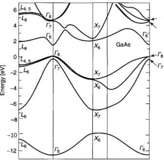
The energy bands depend on the position in the Bnllouin zone, and Fig. 2.15 presents these bands for the intrinsic (i.e., undoped) 111-V compound GaAs. The
t
kzFigure 2.14. Brillouin zone of the gallium arsenide and zinc blende semiconductors showing the
-8 26 - x7 -
Figure 2.1 5. Band structure of the semiconductor GaAs calculated by the pseudopotential method. (From M. L. Cohen and J. Chelikowsky, Electronic Structure and Electronic Properties of Semiconductors, 2nd ed., Springer-Verlag; Solid State Sci. 75, Springer, Berlin, 1989.)
-
x6
-10 -
figure plots energy versus the wavevector k in the following Brillouin zone directions: along A from point
r
to X , along A from to L, along C fromr
to K , and along the path between points X and K . These points and paths are indicated in the sketch of the Bnllouin zone in Fig. 2.14. We see from Fig. 2.15 that the various bands have prominent maxima and minima at the central pointr
of the Bnllouin zone. The energy gap or region where no band appears extends from the zero of energy at point Ts to the point r6 directly above the gap at the energyEg
= 1.35eV. The bands below point Ts constitute the valence band, and those above point r6form the conduction band. Hence Ts is the lowest energy point of the conduction band, and Ts is the highest point of the valence band.2.2. ENERGYBANDS 25
band at point Ts can become thermally excited to point r6 in the conduction band
with no change in the wavevector k. The compounds GaAs, GaSb, InP, I d s , and InSb and all the 11-VI compounds included in Table B.6 have direct gaps. In some semiconductors such as Si and Ge the top of the valence band is at a position in the Brillouin zone different from that for the bottom of the conduction band, and these are called indirect-gap semiconductors.
Figure 2.16 depicts the situation at point
r
of a direct-gap semiconductor on an expanded scale, at temperatures above absolute zero, with the energy bands approximated by parabolas. The conduction band valley at r6 is shown occupiedby electrons up to the Fermi level, which is defined as the energy of the highest occupied state. The excited electrons leave behind empty states near the top of the valence band, and these act like positive charges called “holes” in an otherwise full valence band. These hole levels exist above the energy -E;,, as indicated in Fig. 2.16. Since an intrinsic or undoped semiconductor has just as many holes in the valence band as it has electrons in the conduction band, the corresponding volumes filled with these electrons and holes in k space are equal to each other. These electrons and holes are the charge carriers of current, and the temperature dependence of their concentration in GaAs, Si, and Ge is given in Fig. 2.17.
In every semiconductor listed in Table B.6, including Si and Ge, the top of its valence band is at the center of the Brillouin zone, but the indirect-bandgap semiconductors Si, Ge, AlAs, AlSb, and GaP have the lowest valley of their conduction bands at a different location in k space than the point
r.
This is shown in Fig. 2.18 for the indirect-bandgap materials Si and Ge. We see from Fig. 2.18b that Ge has its conduction band minimum at the point L, which is in the middle of the hexagonal face of the Brillouin zone along the A or (1 1 1) directionFigure 2.16. Sketch of lower valence band and upper conduction band of a semiconductor approximated by parabolas. The region in the valence band containing holes and that in the
conduction band containing electrons are cross-hatched. The Fermi energies EF and E;, mark
the highest occupied level of the conduction band and the lowest unoccupied level of the valence band, respectively. The zero of energy is taken as the top of the valence band, and the direct-
2v
1 400500
1,000
1ol8 io16 1014 io12 io1O i o 8 i o 6
n (ern")
Figure 2.17. Temperature dependencies of the intrinsic carrier density of the semiconductors Ge, Si, and GaAs. Note the lack of linearity at the lower temperatures arising from the T3I2 factor in Eq. (2.1 5). (From G. Burns, Solid State Physics, Academic Press, Boston, 1985, p. 31 5.)
depicted in Fig. 2.14. The Brillouin zone has eight such faces, with each point L shared by two zones, so the zone actually contains only four of these points proper to it, and we say that the valley degeneracy for Ge is 4. The semiconductor Si has its lowest conduction band minimum along the A or (001) direction about 85% of the way to the
X
point, as shown in Fig. 2.16. The compound Gap, not shown, also has its corresponding valley along A about 92% of the way toX.
We see from Fig. 2.14 that there are six such A lines in the Brillouin zone, so this valley degeneracy is 6. Associated with each of the valleys that we have been discussing, at point L for Ge and along direction A for Si, there is a three-dimensional constant-energy surface in the shape of an ellipsoid that encloses the conduction electrons in the corresponding valleys, and these ellipsoids are sketched in Figs. 2.19a and 2.19b for Ge and Si, respectively.Some interesting experiments such as cyclotron resonance have been camed out to map the configuration of these ellipsoid-type constant-energy surfaces. In a cyclotron resonance experiment conduction electrons are induced to move along constant energy surfaces at a velocity that always remains perpendicular to an applied magnetic field direction. By utilizing various orientations of applied magnetic fields relative to the ellipsoid the electrons at the surface execute a variety of orbits, and by measuring the trajectories of these orbits the shape of the energy surface can be delineated.
2.2. ENERGY BANDS 27
A X '
Wavevector A
Si
c
z
Ge
(a)
Figure 2.19. Ellipsoidal constant-energy surfaces in the conduction band of germanium (left)
and silicon (right). The constant energy surfaces of Ge are aligned along symmetry direction A
and centered at symmetry point L. As a result, they lie half inside (solid lines) and half outside (dashed lines) the first Brillouin zone, so this zone contains the equivalent of four complete energy surfaces. The surfaces of Si lie along the six symmetry directions A (i.e., along fk,, f k y , fk,), and are centered 85% of the way from the center point
r
to symmetry pointX. All six of them lie entirely within the Brillouin zone, as shown. Figure 2.14 shows the positions of symmetry points I?, L, and X , and of symmetry lines A and A, in the Brillouin zone. (From G. Burns, Solid State Physics, Academic Press, Boston, 1985, p. 313.)
2.2.4. Effective Masses
On a simple one-dimensional model the energy E of a conduction electron has a quadratic dependence on the wavevector k through the expression
h2k2 E = -
2m*
The first derivative of this expression provides the velocity u
- 0
1dE fik f i d k - m *
and the second derivative provides the effective mass m*
1 d2E 1
fi2 dk2 - m*
-- -
-
(2.10)
(2.11)