This document contains information that is proprietary to MIPS Technologies, Inc. MIPS Technologies, Inc. reserves the right to change any products described herein to improve the function or design. MIPS Technolgies, Inc. does not assume any liability aris-ing out of the application or use of any product or circuit described herein; neither does it convey any license under patent rights nor imply the rights of others.
Copyright 1993 by MIPS Technologies, Inc. All rights reserved. No part of this document may copied by any means without written permission from MIPS Technologies, Inc.
MIPS Technologies Inc. 2011 N Shoreline Blvd
PO Box 7311
Mountain View, CA 94039-7311 January 24, 1995
1
January 24, 1995 R4400PC/SC Errata, Processor Revision 2.0 & 3.0
Note: Change bars in the left column indicate corrections or changes from the last revision of the errata.
1. R4400 PC, R4400 SC: The PIdx field of the CP0 register CacheErr, may be loaded with an undefined value
on primary cache data parity errors.
Workaround: When a primary data cache parity error is detected (and a cache error exception is taken), all
possible values of PIdx must be used to check for parity errors in the primary data cache. In the R4400, with a 16K primary data cache, there are four values for the primary data cache index that must be checked.
2. R4400 PC, R4400 SC: The 64bit address space for kernel mode is not correctly decoded. Addresses that
should be reported as address error exceptions may cause tlb refill exceptions instead (as they will not be correctly decoded as outside the range of kernel mode address space). The adddress region effected by this is the xkseg region as defined in the MIPS III architecture (address range0xc000000000000000
-0xc00000ff7fffffff). This region is extended to the range0xc000000000000000
-0xc00000ffffffffff.
Workaround: There is no workaround for this problem - kernel mode may access this expanded region.
3. R4400PC, R4400SC: The R4400 does not take a Reserved Instruction Exception on the "rfe’ instruction. The
R4400 executes a "noop" and kills the following instruction.
Workaround: There is no workaround for this problem.
4. R4400PC, R4400SC: The "dmtc0" and "dmfc0" instructions do not cause a Reserved Instruction Exception
in User or Supervisor mode. These instructions will complete successfully.
Workaround: There is no workaround for this problem.
5. R4400PC, R4400SC: Reduced power mode is not available in the current revision of the R4400. Setting the
RP bit in the Status register has no effect on the operation of the R4400.
6. R4400SC: The R4400 always uses sequential ordering regardless of the state of the mode bit which specifies
subblock or sequential ordering.
7. R4400SC: The TWr2Dly parameter is always 1 more than the number programmed. Thus, the range of
TWr2Dly is 2 to 4 PCycles instead of 1 to 3 PCycles.
Workaround: There is no work around for this problem except taking the bug into account while
program-ming.
8. R4400PC, R4400SC: The processor will not take Cache Error exception due to PTag Parity Error under the
following condition:
When performing a Hit_Writeback_Inv_D operation on a primary cacheline, with W_Bit=0. It will invalidate the line, ignoring the error. However, it will take cache-error exception, if the cacheline is inconsistent (W_Bit=1).
Workaround: The effect of this bug is very minimal because, in the worst case, the incorrectly invalidated
cacheline will be refetched, when the data is accessed again.
9. R4400PC, R4400SC: NMI does not clear the TLB Shutdown (TS) Bit in the Status Register (SR[21]). Workaround: There is no work around for this problem.
10. R4400PC, R4400SC: If an NMI is accepted by the processor when it is in any type of stall, the address of the
instruction in the WB stage is transferred into EPC and the instruction is killed. However, if the stalled instruction involves a write into the register file, the processor is unable to stop the write. Upon returning from NMI exception handler, the processor re-executes the killed instruction; thus, causing the write into the same register again. The extra write into the register might cause an erroneous result, if the instruction uses same register as the source and the destination.
Workaround: There is no work around for this problem.
11. R4400PC, R4400SC: When data is moved from the Random register to a general purpose register (using
MFC0), the result in the destination register, erroneously, ends up to be one less (for example, if the Random register has a value N, the destination register ends up with a value N-1). However, the TLBWR instruction which uses the value from Random register to index into the TLB-array, gets the value N and thus writes into the correct TLB-entry at all times.
Workaround: Adjust the destination data of the instruction MFC0, when the source is Random register.
12. R4400PC, R4400SC: The processor, incorrectly, sets the EXL bit in the status register when an exception is
caused by the NMI.
Workaround: There is no work around for this problem.
13. R4400PC, R4400SC: The J and JAL instructions functions incorrectly in certain cases, as described below.
J or JAL instruction causes the processor to unconditionally jump an address which is formed by shifting left, by two bits, the 26 bit target address provided by the instruction; and by concatenating, at the left end, the high order bits of the address of the delay slot.
The concatenation of the high order bits of the address of the delay slot means that these instructions can only cause a jump within the 256Mbyte region where the delay slot instruction is located.
The bug occurs when a J, or JAL instruction falls in any of the 3 words before the last word in a 256Mbyte region (the words marked j below):
0x0ffffff0 j 0x0ffffff4 j 0x0ffffff8 j 0x0ffffffc
--- 256Mbyte region boundary 0x10000000
or:
0x1ffffff0 j 0x1ffffff4 j 0x1ffffff8 j
3
January 24, 1995 R4400PC/SC Errata, Processor Revision 2.0 & 3.0
0x1ffffffc
--- 256Mbyte region boundary 0x20000000
..., etc.
In these cases, the high order bits are taken from the next 256Mbyte region generating a destination address that is 256Mbytes beyond the address that was intended.
Workaround: When assigning addresses, the case of a jump on the boundary of a 256Mbyte region
al-ready has to be made a special case as it will form a destination address in the next 256Mbyte region (due to the delay slot already being in the next 256Mbyte region). To workaround this bug, the same address check has to be performed for jumps(j or jal) within the last 4 words of the 256Mbyte region, instead of just the last word.
14. R4400PC, R4400SC: It is possible for the processor to, erroneously, miss detection of a timer interrupt. A
timer interrupt is signalled when the Count register becomes equal to the Compare register (if timer interrupt is enabled by the appropriate mode bit). However, if the Count register is read (using mfc0 rx, C0_COUNT) at the time when it’s value is equal to that of the Compare register, then the read might inhibit the interrupt.
Workaround: If the Count register is only read when setting up a new timer interrupt then no other action
is required. However, if the Count register is read for any other reason, during the period when a valid timer interrupt is expected, then the software needs to check if the Count value that was read is within a few cycles of the Compare value, in which case the timer interrupt might have been lost.
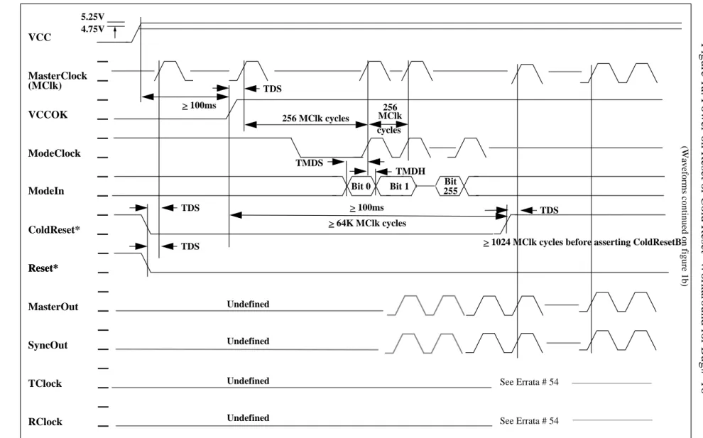
15. R4400PC, R4400SC: During the power up sequence, the period of TClk and RClk may not be as expected
for at least 1024 MasterClock cycles following the de-assertion of ColdResetB. The above bug is true for all system interface divisors. Furthermore, if the system interface divisor other than 2 (i.e. 3,4,6 & 8) is used, TClk and RClk’s rising edge may not align to the rising edge of the MasterClock, as specified.
This may not be a problem for systems using only TClk for the external logic. However, certain systems like
-1) systems using MasterClock for the external logic
2) system with external PLL which needs to lock with the internal PLL 3) systems with multiple processors operating in lock-step
this bug may cause problems.
Thus, for system with interface divisor set to two, the only violation will be that the TClk and RClk’s period might not be valid within 64 MasterClock after the ColdResetB is de-asserted.
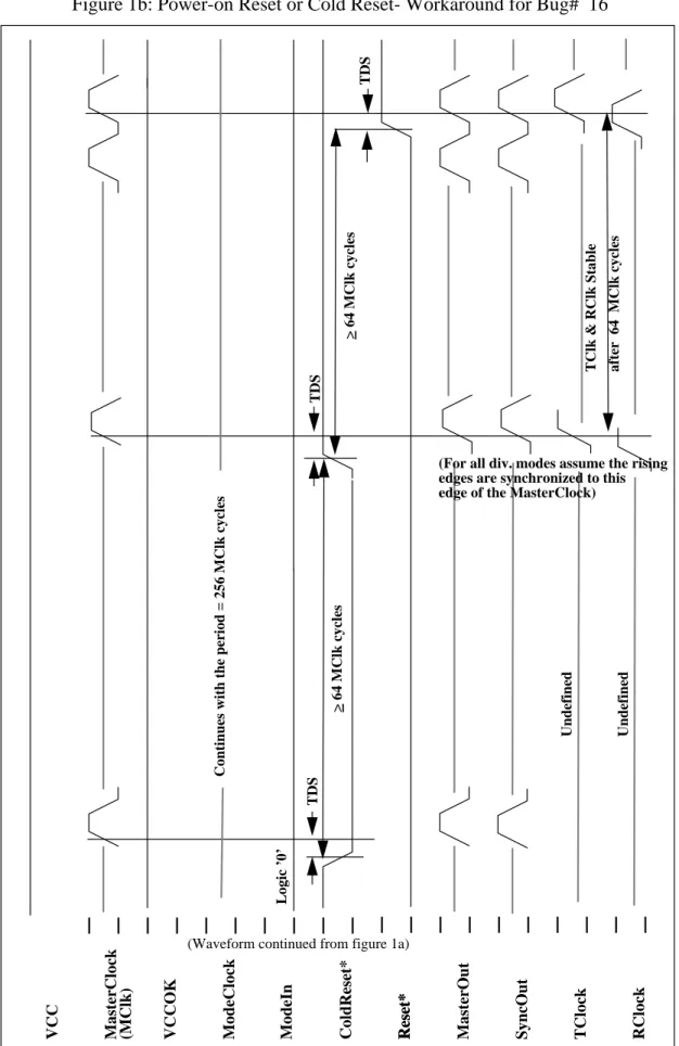
Workaround: Assert a second ColdResetB after at least 1024 MasterClock cycles from the de-assertion
of the first ColdResetB. ResetB should remain asserted until at least 64 MasterClock cycles following the de-assertion of the second ColdResetB. TClk and RClk will then be valid 64 MasterClock cycles after the de-assertion of the second ColdResetB and their edge alignment with respect to MasterClock will be as spec-ified. Figure 1a & 1b show the waveforms in more detail. Note that the waveforms in Figure 1b are contin-uation of the those in figure 1a.
4
January 24, 1995
Figure 1a: Power-on Reset or Cold Reset- Workaround for Bug# 16
MasterClock VCCOK ModeClock ModeIn ColdReset* Reset* MasterOut SyncOut TClock RClock TDS Undefined Undefined Undefined Undefined VCC TMDS > 100ms TDS 256 MClk cycles 5.25V 4.75V TDS > 100ms Bit 0 TMDH > 64K MClk cycles Bit TDS Bit 1 256 cycles MClk Reset* (MClk) 255
> 1024 MClk cycles before asserting ColdResetB
(Waveforms continued on figure 1b)
See Errata # 54
5
January 24, 1995 R4400PC/SC Errata, Processor Revision 2.0 & 3.0
Figure 1b: Power-on Reset or Cold Reset- Workaround for Bug# 16
MasterClock VCCOK ModeClock ModeIn ColdReset* Reset* MasterOut SyncOut TClock RClock
TDS
Undefined Undefined
VCC
TDS
Continues with the period = 256 MClk cycles
TDS
> 64 MClk cycles
> 64 MClk cycles
Reset*
(MClk)
(Waveform continued from figure 1a)
Logic ’0’
TClk & RClk Stable
(For all div. modes assume the rising
after 64 MClk cycles
edges are synchronized to this edge of the MasterClock)
16. R4400PC, R4400SC: The CacheOp instructions are encoded as a primary d-cache stall (’a’) on the status
pins regardless of the cache (I, D, SI or SD) it is operating on. Also, the final run cycle of any Cache Op shows up as code ’1’ on the status pins. This means that there is no way to differentiate between the CacheOp and a load instruction that had a primary data cache miss by looking at the status pins.