Modelling Methods for Testability Analysis of Analog
Integrated Circuits Based on Pole-Zero Analysis
Der Fakultät für Ingenieurwissenschaften der
Universität Duisburg-Essen
zur Erlangung des akademischen Grades eines
Doktor-Ingenieur
(Dr.-Ing.)
vorgelegte Dissertation
von
Hasan Albustani
aus
Hama/Syrien
Referent: Prof. Dr.-Ing. Axel Hunger
Korreferent: Prof. Dr-.Ing. Bernd Straube
Abstract
Analog and mixed-signal circuits are gaining popularity in various applications such as tele-communication, multimedia, biomedical applications and others. Testing of these circuits has a major impact on product cost and time-to-market. Furthermore, the trend of integrating com-plete analog/digital systems on a single chip has resulted in new testing challenges for such systems.
Testability analysis for analog circuits provides valuable information for designers and test engineers. Such information includes a number of testable and nontestable elements of a cir-cuit, ambiguity groups, and nodes to be tested. This information is useful for solving the fault diagnosis problem.
In order to verify the functionality of analog circuits, a large number of specifications have to be checked. However, checking all circuit specifications can result in prohibitive testing times on expensive automated test equipment. Therefore, the test engineer has to select a finite subset of specifications to be measured. This subset of specifications must result in reducing the test time and guaranteeing that no faulty chips are shipped.
This research develops a novel methodology for testability analysis of linear analog circuits based on pole-zero analysis and on pole-zero sensitivity analysis. Based on this methodology, a new interpretation of ambiguity groups is provided relying on the circuit theory. The testability analysis methodology can be employed as a guideline for constructing fault diagnosis equa-tions and for selecting the test nodes.
We have also proposed an algorithm for selecting specifications that need to be measured. The element testability concept will be introduced. This concept provides the degree of difficulty in testing circuit elements. The value of the element testability can easily be obtained using the pole sensitivities. Then, specifications which need to be measured can be selected based on this concept. Consequently, the selected measurements can be utilized for reducing the test time without sacrificing the fault coverage and maximizing the information for fault diagnosis.
Acknowledgments
I would like to take this opportunity to thank Prof. Dr.-Ing. B. Straube from Fraunhofer Insti-tute Branch Lab Design Automation in Dresden for his support and patience. I would like also to thank all members of the Test and Verification group, especially, Dr.-Ing W. Vermeirn for his guidance and valuable advice throughout this research.
I would like to express my gratitude to Prof. Dr.-Ing. A. Hunger for his supervision.
Finally, I would like to thank my wife Maram and my son Adir for their encouragement and support.
Table of Contents
Chapter 1
Introduction . . . .
1
1.1. Analog Test Philosophy . . . . 1.2. Motivation and Problem Definition . . . . 1.3. Organization . . . .
1 3 5
Chapter 2
Circuit Modeling and Simulation . . . .
7
2.1. Introduction . . . . 2.2. Circuit Modeling . . . . 2.3. Simulation Techniques . . . . 2.3.1. Event-Driven Simulation . . . . 2.3.2. Time-Continuous Simulation . . . . 2.3.3. Mixed-Mode Simulation . . . . 2.4. Circuit Simulation . . . . 2.4.1. Circuit Topology . . . . 2.4.2. Circuit Equations Formulation and Solution . . . . 2.4.3. Analog Circuit Analyses . . . .
2.4.3.1. DC Analysis . . . . 2.4.3.1. AC Small Signal Analysis . . . . 2.4.3.1. Transient Analysis . . . . 2.4.3.1. Sensitivity Analysis . . . . 2.5. Symbolic Modeling. . . . 7 7 10 10 11 11 12 12 14 16 16 17 18 21 23
Chapter 3
An Introduction to Testing of Analog Circuits . . . .
25
3.1. Difficulties with Testing of Analog Circuits . . . . 3.2. Test Flow. . . . 3.4. Fault Classification . . . . 3.3. Testing Techniques . . . . 3.2.1. Specification-Driven Test . . . . 3.2.2. Fault-Driven Test . . . . 3.5. Analog Test Issues . . . . 3.5.1. Analog Fault modeling. . . . 3.5.2. Analog Fault Simulation . . . . 3.5.3. Test Signal Generation . . . . 3.5.4. DSP-Based Testing . . . . 3.5.5. Design for Testability (DfT) . . . . 3.5.5.1. Reconfiguration-Based DfT. . . . 3.5.5.2. Accessibility-Based DfT. . . . 3.5.6. Built-In Self-Test (BIST). . . . 3.5.7. Fault Diagnosis. . . . 3.5.8. Testability Analysis . . . . 3.5.9. Test and Measurement Selection. . . .
25 27 30 31 31 33 34 34 36 37 39 41 41 41 44 46 48 52
Chapter 4
Testability Analysis for Analog Circuits . . . 54
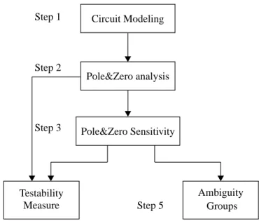
4.1. Introduction . . . . 4.2. Methodology . . . . 4.2.1. Circuit Modeling . . . . 4.2.1.1. Modified Nodal Analysis . . . . 4.2.1.2. State-Variable Equations . . . . 4.2.2. Pole-Zero Analysis . . . . 4.2.3. Pole-Zero Sensitivity. . . . 4.2.4. Testability Measure . . . . 4.2.5. Ambiguity Group Analysis . . . . 4.2.6. Testability Analysis and Controllability/Observability. .
54 56 57 57 58 60 64 67 71 74
4.3. Simulation Examples . . . . 4.3.1. The 7-RC Ladder Circuit . . . . 4.3.2. Continuous-Time State-Variable Filter . . . .
4.3.3. Leapfrog Filter. . . . 4.3.4. The 5-Pole (100Hz) Low-Pass Filter . . . . 4.4. Generalization of the Testability Analysis Algorithm . . . . 4.5. Summary . . . . 75 75 78 83 85 87 89
Chapter 5
Element Testability and Measurement Selection for
Second- Order Circuits . . . .. . . 91
5.1. Introduction . . . . 5.2. The Algorithm . . . .. . . . 5.2.1 Mathematical Representation of Prototype
Second-Order Circuits . . . . 5.2.5 Pole and Zero Sensitivity . . . .
5.2.6 Element Testability and Measurement Selection . . . . 5.3. Simulation Examples . . . . 5.3.1 Continuous-Time State-Variable Filter . . . . 5.3.2 Sallen-Key Bandpass Filter . . . . 5.4. Summary . . . .. . . . 91 92 93 97 97 98 98 106 112
Chapter 6
Element Testability and Measurement Selection for
Higher-Order Circuits . . . 117
6.1. Introduction . . . . 6.2. The Algorithm . . . .. . . . 6.2.1. Dominant Poles . . . . 6.2.2. Model-Order Reduction . . . . 6.2.2.1. Moment Generation . . . . 6.2.2.2. Moment Matching . . . . 6.2.3. Pole and Zero Sensitivity Calculation in AWE. . . . 6.2.4. Element Testability and Measurement Selection. . . . 6.3. Simulation Examples . . . . 6.3.1. RLC Circuit . . . . 6.3.2. Leapfrog Filter . . . . 113 113 115 116 116 118 119 122 123 123 1276.4. Discussion . . . . 6.5. Summary . . . .
131 131
Chapter 7
Testability Analysis of Nonlinear Circuits . . . .
132
7.1. Introduction . . . . 7.2. Testability Analysis Algorithm . . . . 7.2.1. Circuit Linearization and Description . . . . 7.2.2. Pole and Zero Analysis . . . . 7.2.3. Pole and Zero Sensitivity . . . . 7.2.4. Ambiguity Groups . . . .. . . . 7.2.5. Frequency-Domain Specifications . . . . 7.2.5.1. The Low-Frequency Response . . . . 7.2.5.2. The High-Frequency Response . . . . 7.2.6. Parameter Testability and Measurement Selection . . . . 7.3. Simulation Examples . . . .
7.3.1. The Simple Common-Emitter Amplifier . . . . 7.3.2. The CMOS Differential Amplifier . . . . 7.3.3. The Operation AmplifierµA741 . . . . 7.4. Summary . . . . 132 133 134 135 135 136 136 138 141 139 140 140 146 149 151
Chapter 8
Conclusion . . . .
152
8.1. Original Contributions . . . . 8.2. Recommendations for Future Research . . . .154 155
Appendix A
. . . .
156
A.1. Adjoint Methods for Sensitivity Computation. . . . A.2. Sensitivity Computation Using Saber Simulator. . . . A.3. Sensitivity Properties . . . . A.4. Sensitivities of Natural Response, Time-Domain and
Frequency -Domain Specifications for Second-Order Circuits 156 158 160
161
Chapter 1
Introduction
1.1. Analog Test Philosophy
Testing of analog and mixed signal circuits has become a challenge and gained more interest in the last decade for many reasons including increasing the applications of the analog circuits, integrating the whole system on one chip, and the high cost of analog testing compared with digital testing counterpart.
The reason for increasing the analog circuit applications is due to signals in real world are ana-log in nature with a continuous amplitude and time scale. Thus, any electronic system which interacts with the outer world has to contain some analog interface circuitry. Many domains such as telecommunications, multimedia, and biomedical applications require such analog interface circuitry. Analog and mixed-signal circuits such as amplifiers, filters, switches, ana-log-to-digital, and digital-to-analog converters are required in many end-equipment applica-tions such as cellular telephones, hard-disk drives, modems, motor controllers, and multimedia audio and video products. Moreover, the analog circuits provide a good overall performance for high-performance applications (high frequency and low power applications), low-noise data-acquisition systems (e.g. in biomedical sensor applications), and parallel analog signal processing (such as in neural networks with a huge number of neurons). The strategy for test-ing these analog and mixed signal circuits (interface circuitry) is still needed.
In the past, a chip was just a component of a system; today, a chip is a system in itself. This integration of a system including analog and digital circuits in a chip (system-on-a-chip SoC)
has posed non-trivial problems in design and test areas. There are many factors that cause the complexity in testing the system-on-a-chip (SoC). Such factors are [Claa03]: the lack of ade-quate fault models, incapable tools for coping with the complexity of the SoC, lack of accessi-bility (lack of controllaaccessi-bility and observaaccessi-bility), lack of an industrial standard analog design for testability (DfT) methodology, and raising the importance of the timing-related faults. The test cost of analog and mixed-signal circuits has now increased in comparison with digital test cost as shown in Figure 1-1 [Robe01]. The high analog test cost results from many factors such as expensive test equipment, long test development time, and long test production time. The development and production test time costs constitute a part of the development and pro-duction costs of the integrated circuits (ICs), respectively. Both the development and produc-tion test time are related to the time-to-market (TTM) which plays an important role for competitive semiconductor companies.
The challenge which test engineers are faced with is to develop a test methodology in order to reduce the test cost and to accelerate the time-to-market without sacrificing IC quality.
Consequently, the generation and evaluation of an effective test methodology is a very impor-tant issue in the production of an IC that having direct consequences on the price and the qual-ity of the final product.
Figure 1-1: Electronic Manufacturing/ Test Cost [Robe01] Digital Test
Analog Test Manufacturing
(design, assembly & parts)
Analog Test Manufacturing
(design, assembly & parts)
Digital Test
Relative Product Costs (Present)
Relative Product Costs (Future)
1.2. Motivation and Problem Definition
Testing can be defined as the process of verifying that an IC meets the specifications for what was designed [Huer93a]. Thus, the primary need for testing is to perform the following two sequential tasks:
(1) Checking the design characterizations: this task is called prototype testing. (2) Checking manufacturing defects: this task is called production testing.
The objective of prototype testing is to verify the circuit under test (CUT) characterizations. If the circuit under test is identified as faulty during design characterization before it is sent to mass-production, it is desirable to diagnose the cause of the failure. Once faults are identified and located, a circuit can then be redesigned to enhance the yield of the ICs.
Prior information is required before fault diagnosis can be attempted. Such information includes optimal test points, optimal measurements, ambiguity groups, testable elements (which can be isolated), and untestable elements (which are assumed to be nominal). This information can be obtained by testability analysis of the circuit under test (CUT). The con-cept of testability analysis is strictly tied to the concon-cept of the element-value solvability prob-lem, which gives information about the solvability of the test problem for linear analog circuits. The degree of solvability of the circuit under test can be quantified using testability
measure concept. As a result, the testability measure allows us to know beforehand how many
faulty elements can be identified and how many elements have to be assumed fault-free. The testability measure is quantitatively given by the rank of the sensitivity matrix (testability matrix) constructed from the derivation of output parameters with respect to circuit elements. In low testability circuits, where the testability measure is less than the number of the circuit elements, the testability analysis is strictly tied to the ambiguity group concept. Ambiguity groups consist of circuit elements that produce the same values of measurements. Therefore, the ambiguity groups have to be identified before constructing the fault diagnosis equations. The ambiguity groups can be determined by finding the null space of the testability matrix, in other words by finding the linearly dependent columns of the testability matrix. The zero-value rows of null space matrix correspond to the definitely testable elements and the nonzero-value rows and not orthogonal correspond to the elements that belong to the same ambiguity group. The null space of the testability matrix can be computed by QR factorization or by sin-gular value decomposition (SVD) of the testability matrix.
The target of production testing is to detect defects resulting from the imperfections of the manufacturing process. Production testing is performed to distinguish good circuits from faulty ones. Testing cost (reflected as test time, throughput, and the cost of automatic test equipment) is a major concern for production testing. In order to make the decision whether a circuit is faulty or fault-free, a large number of specifications have to be checked. Thus, it is not possible to perform an exhaustive test, since it will require an infinite number of measure-ments and may result in prohibitive testing times on expensive automated test equipment. Therefore, the test engineer has to select a finite subset of specifications to be measured. This subset of specifications must result in reducing the test time and guarantee that no faulty chips are shipped.
Selecting an optimal set of measurements is related to the objective of a test. For example, if the goal of a test is only to detect faults, the selected measurements have to guarantee high fault coverage and reduce the test time. On the other hand, if the goal of a test is to locate faults, the selected measurements have to distinguish faulty elements from good ones taking into account ambiguity groups.
In this thesis, we will address two problems. The first one is to determine a testability measure (the number of testable elements) and ambiguity groups. The second one is to select the mini-mum number of measurements which lead to the reduction of the time cost without sacrificing fault coverage. Our measurement selection algorithm can also be employed in breaking up ambiguity groups should the fault diagnosis be the goal of the test.
In the first part of the thesis, we will present a novel methodology for determining the testabil-ity measure and ambigutestabil-ity groups based on the poles and zeros of the transfer function which represents the linear analog circuit. Unlike other methods, which require numerical methods such as QR or SVD decompositions, our methodology requires only the knowledge based on the circuit theory. Thus, a new interpretation for the testability measure and ambiguity groups is presented which depends on the poles and zeros of the linear analog circuit. The proposed methodology can be employed as a guideline for fault diagnosis and test node selection. Furthermore, the relationship between the testability measure based on the pole and zero anal-ysis and controllability/observability concepts from control theory will be discussed. The con-trollable (or non-concon-trollable) and observable (or non-observable) states in linear analog circuits can be determined based on pole and zero sensitivity.
In the second part of the thesis, the problem of minimizing the cost of production testing is considered. We will introduce the element testability concept which can be defined as the rela-tive degree of difficulty in testing circuit elements with respect to circuit specifications under the parametric faults conditions. The element testability is computed based on the sensitivities of the poles and zeros of the linear or linearized analog circuit. Thus, our method depends on the sensitivity analysis which provides the relationship between the circuit elements and per-formance specifications. This kind of analysis ensures the structural and the functional test; in other words the circuit elements are tested by verifying circuit functionality. The selected mea-surements can be utilized for
• obtaining the high fault coverage or evaluating the test vectors in a fault simulator,
• reducing the test cost by reducing the number of tests without affecting the fault coverage, and
• for breaking up the ambiguity groups if the fault diagnosis is the goal of a test.
1.3. Organization
This thesis is organized as follows:
In Chapter 2, modeling and simulation of analog circuits will be discussed. Circuit modeling is presented using the levels of abstraction and hierarchy concepts. Furthermore, we will address simulation techniques used for simulating digital, analog, and mixed-signal circuits. Finally, a general overview of circuit simulation will be discussed.
In Chapter 3, a general introduction to testing analog and mixed-signal circuits will be addressed. The complexity of analog circuit testing and design-test flow will be discussed. Then, the analog testing techniques, namely the specification-driven test and fault-driven test, will be given. The classification of faults which can occur in analog circuits is discussed. Finally, we will present the state of the art for analog and mixed-signal circuit testing.
In Chapter 4, a new methodology for testability measure and ambiguity group determination will be presented. This methodology is based on the well-known pole and zero analysis and on pole-zero sensitivity. The testability measure at a certain node of a circuit can be computed from the number of the poles and zero in addition to the DC gain of the transfer function. Also, the testability measure can be computed from the circuit matrix constituted using the modified nodal analysis. The ambiguity groups can be determined using the pole and zero sensitivity.
Thus, a new interpretation of the ambiguity groups will be given based on the knowledge of the circuit theory. In this chapter, various simulation examples will be presented in order to validate our method.
In Chapter 5, we will present an algorithm for measurement selection for linear second-order circuits. The aim of this algorithm is to maximize the fault coverage and to reduce test cost by reducing the number of specifications that need to be measured. Also, this algorithm can pro-vide maximum information about fault identification for fault diagnosis by breaking up the ambiguity groups. This algorithm is based on the element testability concept which can be determined based on the sensitivity of the circuit poles. The element testability will provide the information about the difficulty in testing circuit elements as well as the effect of element changes on circuit specifications. Parametric faults which are caused by manufacturing pro-cess variations and do not affect the circuit topology will be considered in this chapter.
In Chapter 6, the element testability and measurement selection algorithm proposed in Chap-ter 5 is developed to cover higher-order circuits. Higher-order circuits will be approximated by second ones using moment matching methods such as asymptotic waveform evaluation (AWE) by which the two complex-conjugate dominant poles of a circuit can be extracted. The element testability concept can be utilized to select specifications that need to be measured. Chapter 7 presents the testability analysis of nonlinear analog circuits. A nonlinear analog cir-cuit is linearized around an operation point and represented by its transfer function in the Laplace domain. The ambiguity groups can be determined based on the sensitivities of the poles and zeros of the linearized circuit. The parameter testability concept which gives an insight into the difficulty of testing the circuit parameters is introduced. Specifications that need to be measured can be selected relying on this concept. The parameter testability of cir-cuit parameters with respect to circir-cuit specifications can be obtained based on the pole sensi-tivities.
The measurement selection algorithm for nonlinear circuits can also be utilized to reduce test time without sacrificing the fault coverage and to provide maximum information for fault identification.
Chapter 2
Circuit Modeling and Simulation
2.1. Introduction
Modeling and simulation are the most important parts of system analysis [Law00]. Modeling is defined as a process by which the physical system can be transformed into an abstract form called model. Simulation is defined as the process by which a computer is used (numerical analysis) to evaluate a model and to estimate its important characteristics. From an electronic circuit point of view, modeling can be employed to transform electrical circuits into a mathe-matical description called model. The model is described by the internal states and the input/ output relationships such as logic equations for digital circuits or differential and algebraic equations (DAEs) for analog circuits [Sale94]. Then, an analog simulator such as SPICE is used to solve the mathematical equations that describe a circuit.
2.2. Circuit Modeling
The levels of abstraction modeling the digital circuits are mature and strictly defined [Ash03]. In contrast, the case of analog circuits is not similar, the levels of abstraction of analog design are not strictly defined, and there is no general agreement in the analog design community about the actual abstraction levels to be used in analog design automation [Giel91, Rose98]. The analog circuits may be modeled in different domains, each domain focusing on different aspects. These domains can be categorized into three perspectives: structure, behavior and
geometry, as shown in Figure 2-1 [Ashe03]. Each of these domains can also be divided into different levels of abstraction. At the upper level, a general overview of these domains is con-sidered, and at the lowest level the greatest amount of details of the system is provided.
The structure domain describes the analog circuits by a composition of interconnected ele-ments or subsystems such as resistors, capacitors, transistors, op-amps, filters and others. The structure domain can be divided into different levels of abstraction: circuit level (also called element level or transistor level), structural macromodel level (also called functional level) and system or chip level.
The circuit level is the lowest level of abstraction and the elements at this level are primitives. At this level, the analog circuits are presented using semiconductor devices (such as BJT and MOSFET transistors) and passive elements (such as resistors and capacitors). There are sev-eral commercial circuit simulators such as SPICE and their derivatives which offer very accu-rate simulation, however, at this level the simulation is a very time-consuming task for large circuits. Therefore, a trade-off between accuracy and speed is accomplished using higher lev-els of abstraction.
The structural macro-model level or functional level consists of a collection of primitive ele-ments such as operation amplifiers and comparators which are designed to achieve a specific functionality. Models at this level can be simplified to produce other models with the same
Figure 2-1: Analog domain and levels of abstraction [Ashe03]
Structural view Behavioral view
Geometry view
Ideal&nonideal equations level Behavioral macromodel level
Transfer function&algorithm level
Circuit (transistor) level Structural macromodel level System (chip) level
function, this technique being known as macromodeling [Mant95]. The model obtained con-sists of fewer elements than the original model of the circuit level description, an example being the Boyle op-amp macromodel [Boyl74]. This leads to short computational time and enables the simulation of larger circuits. The derivation of simplified models can be achieved by several methods such as circuit simplification, circuit build-up, symbolic macromodeling, and a combination of these methods [Mant95].
The system level consists of a connection of functional blocks or system transfer functions such as a modem chip. An example of the structural view is given in Figure 2-2 [Giel91]. The behavior domain describes the system by means of the linear or nonlinear mathematical equations. The detailed structure of the system is undefined. The behavior domain can also be divided into different levels of abstraction, nonideal equations, ideal equations, behavioral macromodel, transfer function, and algorithm [Ashe03].
For analog circuits, the description of the lowest level is provided by differential and algebraic equations (DAEs) with sets of unknowns that are a function of the time. At the highest level, the analog circuits can be modeled by using the transfer functions (for example using Laplace Transform). Hardware description languages such as VHDL-AMS [Ashe03] and MAST [Anal97] can be used to describe analog circuits using the behavioral description.
It is worthwhile to distinguish between the structural macromodel and the behavioral macro-model. The structural macromodel described by primitive elements can be simulated using a circuit simulator like SPICE, and provides more accuracy. In contrast, the behavioral
macro-Figure 2-2: The levels of abstraction for a modem circuit [Giel91] System level Macromodel level Circuit level receiver transmitter modem + -opamp transistor
model described by means of differential equations can be simulated using a behavioral simu-lator based on a behavioral modeling language such as VHDL-AMS. The behavioral macromodeling is still faster than the structural macromodel.
The combination of structural and behavioral modeling can be utilized using different levels of abstraction; this technique is known as multi-level hierarchical modeling. The circuit models can be described at different levels of abstraction. The model of interest is simulated at the lower level with more details (if detailed timing information is desired). The rest of the circuit models are simulated at the higher level to accelerate the simulation (where the accuracy is not the critical issue).
Finally, the geometry domain describes how the system is laid out in physical space (layout). This domain can be also divided into different levels of abstraction [Ashe03].
A progression from the upper level (the system level) to the lowest level (the electrical level) provides an increase in the accuracy of the simulation at the cost of more CPU-time. In con-trast, a progression from the circuit level to the highest levels allows for larger and larger cir-cuits to be simulated for a given amount of CPU-time or requires less and less CPU-time to simulate a given circuit. Multiple levels of abstraction are commonly used in top-down design or bottom-up verification. In both cases, the entire design at any given point in time may be represented at a number of different levels of abstraction [Sale94]. Therefore, mixing different domains and multiple levels would provide an effective balance between simulation speed and accuracy.
2.3. Simulation Techniques
System simulation methods can be classified as event-driven simulation, time-continuous and combined methods, depending on whether the system states are changed continuously or instantaneously [Law00]. In most simulation methods, the major independent variable is time.
2.3.1. Event-Driven Simulation
In event-driven simulation, the signals of interest consist of events which are changed instanta-neously at separated points of time. The events contain the functional and the time information of a system. The event-driven simulation is widely employed in modeling digital hardware and communication systems.
In a digital system, the state variables take certain values called logic levels (e.g. high, low, and unknown). An event is a change in state variables of some circuit nodes that may affect other nodes in the circuit. The effect of an event is to cause all fan-out nodes to be processed and possible new events to be scheduled if changes in their output nodes occur.
Digital signals change their state values instantaneously (at discrete time points). Therefore, a digital simulator only needs to keep track of the timing of these changes (referred to as events) and the value held by a node between events. In order to accomplish this most efficiently, dig-ital simulators employ what is known as an event queue. An event queue is an list ordered according to the occurrence time. “Digital time” progresses by taking each event in order, placing the changed state on a variable, and activating the models that are listed for such an event [Mant95].
2.3.2. Time-Continuous Simulation
In time-continuous simulation, the state variables, which represent the system models, are changed continuously with respect to time. The system can be modeled by ordinary differen-tial equations (ODEs). Thus, a time-continuous simulator is a differendifferen-tial equations solver. Normally, an analytical solution for the models which are represented by means of the nonlin-ear differential equations is not possible in most cases, therefore, numerical integration meth-ods are used. Continuous-time models can usually be used for analog circuits, physical processes, sensors and actuators.
In analog circuits, Kirchhoff’s Voltage Law (KVL), Kirchhoff’s Current Law (KCL) and branch constitutive equations are used to obtain the differential equations. Then, a time-con-tinuous simulator such as SPICE can be used to solve these equations numerically via numeri-cal integration methods. It is also possible in analog circuits to represent the state-variables as a function of frequency instead of time.
As a result, a simulator for continuous analog systems is a solver of simultaneous differential equations while an event-driven simulator is an event manager that activates selected parts of the system sequentially.
2.3.3. Mixed-Mode Simulation
In combined methods, the event-driven methods interact with time-continuous methods to simulate mixed-signal circuits. Such simulation methods that combine event-driven and time
continuous simulations are referred to as mixed-mode simulation. In practice, the implementa-tion of the mixed-mode simulaimplementa-tion can be classified as native mode, glued mode or fully inte-grated mode approaches [Sale94].
The native approach (or core modification approach) is implemented by extending an existing analog or digital simulator to comprehend the levels that are missing. Both, analog and digital algorithms are merged into a single simulator architecture and operate under a single event scheduler. Typically, an analog simulator is extended to incorporate the digital one, since the opposite extension is difficult without major modifications to the original digital simulator. The glued approach actually is implemented using two existing simulators (analog and digi-tal). Such approach must define an interface protocol so that both simulators can communicate with each other effectively. The communication protocol may tend to reduce the speed, and sometimes the accuracy, of the complete simulator. The glued simulator permits using both simulators without any modifications in contrast to the native mode which needs to achieve some modification of the original simulator.
The fully integrated approach is implemented using various simulation algorithms which are connected via well-defined data-transfer/synchronization mechanism called backplane. In this approach, single engine and unified data structure for both analog and digital components are used. The main drawback of this approach is the long development time.
2.4. Circuit Simulation
Circuit simulation is used in circuit design to verify circuit functionality and to obtain detailed timing information before the expensive and time-consuming fabrication process is performed [Bane94].
Circuit simulators provide very accurate electrical waveform information, however, it is impractical and extremely time-consuming for complex analog and mixed-signal VLSI cir-cuits. In fact, a circuit simulator is the only tool which provides enough detail to ensure that a circuit will meet specifications over a wide range of circuit parameters and operation condi-tions [Sale94, Horn99].
2.4.1. Circuit Topology
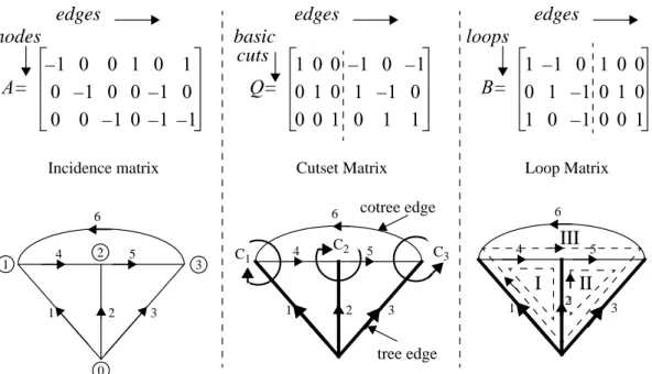
An analog circuit can be described using the graph theory where the circuit elements are repre-sented by the edges of a graph and circuits nodes are reprerepre-sented by the nodes of a graph. The
direction of current flowing through the branches can be assumed from the positive to the neg-ative nodes. An example of the circuit and its associated graph is shown in Figure 2-3 [Vlac94]
There are three matrices associated with a direct graph: incidence matrix A, cutset matrix Q, and loop matrix B as shown in Figure 2-4.
Incidence matrix A is a n x b matrix where n is the number of ungrounded nodes and b the number of edges in the graph. The rank of matrix A is equal to n (Rank(A) = n). The KCL and KVL can be represented using the incidence matrix as Ai = 0 and vb= Atvnrespectively, where
i is the current of branches, vnis node voltages and vb is branch voltages.
A tree of a graph is defined as the edges containing all the nodes of the original network which do not form a closed path. The remaining edges form a cotree. A cut through an edge of the tree and many edges in the cotree form a cutset. Since there are n edges in a tree, there will be
n basis cuts.
The cutset matrix Q (n x b) can be constructed using a set of cuts Qi = 0 and can be written as
Q = [QtQc] or [1 Qc] where Qcand Qtcorresponds to the cotree edges and tree edges respec-tively.
The loop matrix B (n x b) is formed using the fundamental loops in the graph that contain only one cotree edge and many tree edges where Bv = 0. The loop matrix can be partitioned into two matrices B = [BtBc] or [Bt 1] where Bc and Btcorresponds to the cotree edges and tree edges respectively. The cutset matrix and loop matrix are orthogonal BQt = 0 or QBt = 0.
Thus, the loop matrix can be obtained from the cutset matrix and vice versa. Figure 2-3: An example of analog circuit and its associated graph [Vlac94]
R6 J1 C4 C3 R5 R2 1 2 3 4 5 6 1 2 0 1 2 3 3 0 + -+ + + +
-The graph representation of the analog circuits is employed in many applications such as for-mulation of circuit equations and forfor-mulation of state-variable equations [Vlac94].
2.4.2. Circuit Equations Formulation and Solution
There are mainly three formulation methods of circuit equations, namely nodal analysis, mod-ified nodal analysis, and Sparse Tableau analysis [Vlac94].
Classical nodal analysis depends on the KCL for each node to formulate the circuit equations and is given in matrix form as follows:
where Yn is the admittance matrix, V is the node voltages, and J is the independent current sources. However, nodal analysis cannot represent the dependent sources such as current trolled voltage source (CCVS), voltage controlled voltage source (VCVS), and current con-trolled current source (CCCS). Hence, the modified nodal analysis is used to add the ability to present such circuit elements. The modified nodal analysis is now the most common method used in circuit simulators. The underlying idea of modified nodal analysis is to add the current
Figure 2-4: The fundamental matrices and their associated graphs
A 1 – 0 0 1 0 1 0 –1 0 0 –1 0 0 0 –1 0 –1 –1 = Q 1 0 0 –1 0 –1 0 1 0 1 –1 0 0 0 1 0 1 1 = B 1 –1 0 1 0 0 0 1 –1 0 1 0 1 0 –1 0 0 1 = edges nodes edges basic cuts 1 2 3 4 5 6 1 2 3 0 1 2 3 4 5 6 C3 C2 C1 edges loops 1 2 3 4 5 6 I II III
Incidence matrix Cutset Matrix Loop Matrix
Cutsets
tree edge cotree edge
Loops
of elements which do not have an admittance description. The matrix form of modified nodal analysis is given:
where Yn is the admittance matrix, B, C, and D are matrices which are resulted from the new equations that describe the non-conductive elements (contain only -1, 1, and 0), V is the node voltages and I is the branch currents of the non-conductive elements, J and E are the indepen-dent current and voltage sources respectively. Also, the system equations can be expressed as
Yx = b, where Y is the system matrix created by modified nodal analysis, x is the solution
vec-tor which can be composed of currents and voltages and b is the source vecvec-tor.
The third method of circuit equation formulation is Sparse Tableau in which all branch cur-rents, all branch voltages, and all nodal voltages are retained as unknown variables of a circuit. The matrix form of Sparse Tableau is given by Eq. (2-3)
where 1 is the identity matrix, A is the incidence matrix, Yb and Zb are the admittance and impedance matrices respectively, Vbis the branch voltages, Ibis the branch currents, Vnis the branch voltages, and Wbis the independent current and voltage sources. The size of the matrix
T is (n+b+b) x (b+b+n) where n is the number of the circuit nodes and b is the number of the
circuit branches.
The solution of the linear system described by the last equations (2-1), (2-2), and (2-3) is per-formed by either direct methods or iterative methods. Direct methods are used to solve the lin-ear equations in a fixed and finite number of steps while iterative methods need to converge to the exact solution by presumed error. Many important factors are contributed to assess the desired method such as complexity of computation, accuracy, and the ease of implementation. The most direct methods used to solve linear system are the Gaussian elimination and the LU decomposition with pivoting strategy to avoid the ill-conditioning problem. These algorithms are employed to perform DC, AC, and transient analysis. Iterative methods such as Gauss-Jacobi, Gauss-Seidel, and relaxation methods are normally used to perform the transient anal-ysis. These methods are faster than the direct methods and provide more information such as
latency (certain circuit signal values do not change appreciably with time) and multirate
Yn B C D V I J E = or Y x = b (2-2) 1 0 –At Yb Zb 0 0 A 0 Vb Ib Vn 0 Wb 0 = or T X = W (2-3)
behavior (signal values in different portions of circuits change at different rates requiring
dif-ferent time steps). Furthermore, they are suited for parallel computing [Bane94].
A nonlinear system is described by nonlinear equations. These nonlinear equations are usually solved by means of the Newton-Raphson algorithm. The Newton-Raphson algorithm can be used to perform nonlinear the DC analysis and can be combined with other algorithms like the
LU decomposition to perform the nonlinear transient analysis.
2.4.3. Analog Circuit Analyses 2.4.3.1. DC Analysis
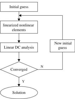
The DC analysis of linear circuits is achieved with shortened inductors and opened capacitors. Also, all time-dependent sources and time-varying parameters and their derivatives are set to zero. The goal of the DC analysis is to determine the DC operating point of the circuit. The operating point defines the steady state of the circuit at time = 0. The DC analysis is automati-cally performed prior to a transient analysis to determine the initial values of the differential equations and prior to the AC small-signal analysis to evaluate the parameters of the linearized small-signal models for nonlinear semiconductor devices. Moreover, the DC analysis can be used to perform the DC transfer (sweep) analysis. The independent source is stepped over a user-specified range, and the DC operation point for a specific output is computed for each DC step.
For nonlinear circuits, the DC operating points are evaluated using iterative methods such as the Newton-Raphson algorithm. The nonlinear elements are linearized around a presumed operation point, and the nodal equations that characterize the linearized circuit are formulated. The linearization about the operating point can be achieved by replacing the nonlinear devices by linear models such as companion model for a diode [Pill95]. Then, the parameters of the linearized model are computed at each iteration. After an initial guess is assumed, the nodal equations are solved at the presumed operation point. Finally, the convergence criteria are checked. If these criteria are fulfilled, the iteration is terminated. Otherwise, the solution is assumed as a new operating point, and the algorithm is again repeated as shown in Figure 2-5 [Pill95]. All problems derived from the iterative algorithms such as iteration step and conver-gence problem (overflow) must be taken into consideration while solving of the nonlinear equations.
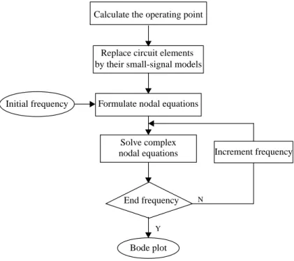
2.4.3.2. AC Small Signal Analysis
In the AC small-signal analysis, the DC analysis is required to determine the parameters of the small-signal model for nonlinear elements. In other words, the nonlinear elements are linear-ized around their operating points and assumed to be operated at the linear region of the input/ output characterization (for example the forward-active region in BJT transistors). Energy storage elements such as capacitors and inductors are modeled in the frequency domain (or Laplace domain) in terms of complex admittances Y (capacitor admittance = jωC or sC,
inductor admittance = 1/jωL or 1 / sL). The linear equations that describe the circuit are
for-mulated. The AC output variables (voltages or currents) are computed by solving the linear equations over a user-specified range of frequencies. The problem which is created by per-forming the AC small-signal analysis at the extreme values of frequency such as ω = 0 (in
which the capacitors become open circuit and the inductors become short circuit),ω--> infin-ity (in which the capacitors become short circuit and the inductors become open circuit), or
frequencies that cause the ill-conditioning problem must be avoided. In the AC small-signal analysis, the behavior of the circuit is evaluated as a function of frequency. The AC small-sig-nal asmall-sig-nalysis can be used to determine the frequency response of the circuit using Bode plot in
Figure 2-5: Newton-Raphson iteration for nonlinear DC analysis Initial guess linearized nonlinear elements Linear DC analysis Converged Solution N Y New initial guess
which the amplitude and the phase of the output variable are evaluated over a range of fre-quencies as shown in Figure 2-6 [Pill95]. Furthermore, the AC small-signal analysis can be utilized to perform the pole-zero analysis, the AC sensitivity analysis, and the noise analysis.
2.4.3.3. Transient Analysis
The transient analysis is used to describe the circuit behavior as a function of time. The electri-cal circuits are represented by differential equations which are formed by means of the Kirch-hoff’s Voltage Law (KVL) or KirchKirch-hoff’s Current Law (KCL) and the constitutive equations. The DC analysis is usually required to determine the initial conditions of the differential equa-tions. There are two approaches to solve the circuit simulation problem: the direct methods and the relaxation-based methods.
In direct methods, the differential equations are converted into linear or nonlinear algebraic equations by means of integration methods such as forward Euler, backward Euler and Trape-zoidal methods. In this step, the time is discretized by a prescribed time step∆t and the energy
storage elements such as capacitors and inductors are replaced by their time-dependent com-panion models [Pill95]. The next step of direct methods depends on whether a circuit is linear or nonlinear. In linear circuits, the integration methods provide directly linear algebraic
equa-Figure 2-6: Small signal AC analysis Calculate the operating point
Solve complex Replace circuit elements
Formulate nodal equations by their small-signal models
nodal equations End frequency Increment frequency Bode plot Initial frequency Y N
tions, whose solution is obtained by Gaussian elimination or LU decomposition at each time point. In nonlinear circuits, the Newton-Raphson algorithm is used for solving the nonlinear equations.
The accuracy plays an important role in transient analysis since the integration methods are an approximation that depends on the selection of time step∆t. Other problems such as
conver-gence speed, initial conditions, stiffness and stability have to be considered.
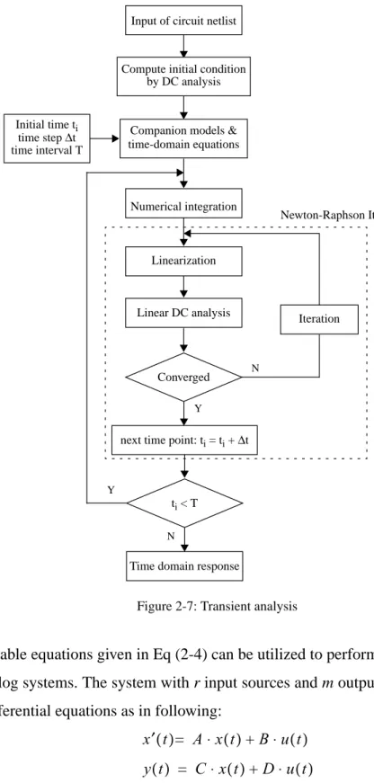
The main disadvantages of the direct methods of the transient analysis are [Ban94]: (1) The excessive computational time needed to compute the response over a long time interval. Two time-consuming processes have to be executed, the Newton-Raphson iteration and solving lin-ear equations (factorization of the Jacobian matrix) at each time point, as shown in Figure 2-7 [Pill95]. (2) The waveform properties such as latency (certain circuit signal values do not change appreciably with time) and multirate behavior (signal values in different portions of circuits change at different rates requiring different time steps) are difficult to exploit. Such properties are often encountered in MOS circuits. Hence, the relaxation-based methods are proposed for solving circuit simulation problems.
The relaxation-based approaches can be divided into three approaches, according to the kind of equations that describe the system [Newt84]. Then, it can be applied for solving linear equations (linear relaxation methods), nonlinear equations (nonlinear relaxation methods), and differential equations (waveform relaxation methods).
The linear relaxation methods are used for solving the linear circuit equations by means of iterative methods such as the Gauss-Jacobi or Gauss-Seidel methods. In these methods, the linear equations are solved for one unknown variable at a time and the other unknown vari-ables are fixed. After iterative solving for unknowns, the final result is convergent to the exact solution. The nonlinear relaxation methods exploit the nonlinear Gauss-Jacobi or nonlinear Gauss-Seidel algorithms combined with the Newton-Raphson algorithm to solve a set of non-linear equations. There are many forms of nonnon-linear relaxation methods such as timing analy-sis, iterated timing analyanaly-sis, and one-step relaxation. Partitioning of the large circuit can be achieved and, by exploiting the parallelism, the nonlinear equations can be solved to acceler-ate the computation [Bane94]. The last kind of relaxation methods is the waveform relaxation method which exploit the Gauss-Seidel procedure for solving the ordinary differential equa-tions.
The state-variable equations given in Eq (2-4) can be utilized to perform the transient analysis for linear analog systems. The system with r input sources and m outputs can be described by first-order differential equations as in following:
where, x(t) is the n x 1 state vector, u(t) is the r x 1 input vector, y(t) is the m x 1 output vector, and matrices A, B, C, D are n x n, n x r, m x n, and m x r, respectively. The state-variable tions can be formulated via network topology based on the direct graph (cutset and loop
equa-Figure 2-7: Transient analysis Input of circuit netlist
Companion models & time-domain equations Initial time ti time step∆t Linear DC analysis Converged N Y Iteration Linearization Newton-Raphson Iterations time interval T
next time point: ti = ti +∆t
ti < T
Time domain response Y
N
Compute initial condition by DC analysis
Numerical integration
x′( )t = A x t⋅ ( )+B u t⋅ ( )
tions) associated to the circuit [Chao95a]. The total response of the circuit can be divided into two responses: zero-state and zero-input responses. The solution of the state-variable (total response) can be obtained via the state transition matrix approach or via the inverse Laplace transform approach.
2.4.3.4. Sensitivity Analysis
The sensitivity analysis is employed in most commercial circuit simulators such as PSpice and Saber. The effect of parameter changes on performance specifications caused by the deviation of the manufacturing process can be determined by using the sensitivity analysis. In other words, the sensitivity analysis based on a first-order approximation provides the variation of a circuit’s response with respect to parameter variations. The performance sensitivity is mathe-matically defined as the derivation of the performance Tj(j=1,2,..., n, where n is the number of circuit performance specifications) with respect to the circuit element hi (i= 1,2,...,k, where k in the number of the circuit elements). The derivatives are computed at the nominal values of the circuit elements. There are two forms of sensitivity, according to the amount of parameter variation. The normalized differential sensitivity (called also small-change sensitivity) is valid only for small deviations (infinitesimal changes) of the element hi(Eq. (2-5)). The normalized incremental sensitivity (also called large-change sensitivity) is used for small and large devia-tions (Eq. (2-7)).
In the case of variation of many output parameters caused by the variation of many elements, the Eq. (2-5) can be expressed in matrix form as follows:
The incremental sensitivity can be expressed as follows:
where∆Tjis the change in performance Tjresulting from an incremental change∆hiof the ele-ment hi. If the circuit performance can be written in rational form as T(s,x) = N(s,x) / D(s,x)
(where s is the complex frequency), then the incremental sensitivity can be computed as a function of the differential sensitivity [Fidl84]:
Sh i Tj hi Tj ---hi ∂ ∂Tj = (2-5) T ∆ T --- S h T ∆h h ---= (2-6) ρh i Tj hi Ti --- ∆Tj hi ∆ ---⋅ = (2-7)
where ShiD is the differential sensitivity of the denominator D of the performance Tj. The incremental sensitivity can be generalized for the deviation in many elements. In the case of the deviation of k elements {h1, h2,..., hk} and one output parameter T, the relative deviation of
output parameter∆T/T can be given by Eq (2-9)
There are two methods for sensitivity computation, namely the direct method and the adjoint method [Dire69] (based on Tellegen’s theorem [Penf70]). In the direct method, the sensitivity of all outputs with respect to one element is needed while in the adjoint method the sensitivity of one output with respect to many parameters is needed. Usually, the sensitivities of all out-puts are not required, or only a single output is available; therefore, the adjoint method is pre-ferred for computing the sensitivity of the output associated with all circuit elements (cf. Appendix A). For the system represented by the modified nodal analysis Yx = b. The adjoint system is represented by Ytxa= - d, where xais the solution of the adjoint system and d is the linear combination of the variables x. The output of interest φ(x) can be expressed asφ= dtx.
The sensitivity of the outputφ associated to the element h can be given:
The cost for the sensitivity adjoint method is equal to that of the two circuit simulations, once for the original circuit and once for the adjoint circuit. The computation of the sensitivities is a time-consuming task, because the sensitivity must be evaluated at each frequency point. Therefore, pole and zero sensitivity provide an alternative for determining the effect of the ele-ment variation on circuit performance, independent of the frequency.
The applications of the sensitivity analysis for analog testing such as fault diagnosis, test sig-nal generation, and test measurement selection will be discussed in Chapter 3, and the applica-tions of the pole and zero sensitivity for the testability analysis and the test measurement selection will be discussed in chapters 4, 5, 6, and 7.
ρh i Tj Shi Tj 1 Sh i D ∆hi hi ---+ ---= (2-8) T ∆ T ---Sh i Tj ∆hi hi ---i=1 k
∑
1 Sh i D ∆hi hi ---i=1 k∑
+ ---= (2-9) h ∂ ∂φ xa ( )t h ∂ ∂Y x ( )xat h ∂ ∂b – = (2-10)2.4.4. Symbolic Modeling
Symbolic modeling of analog circuits is usually achieved at the circuit level of abstraction to generate a closed-form analytical expression for circuit characteristics as a function of inde-pendent variables (time or frequency) with a part or all of circuit’s elements represented by a symbol [Giel94]. This allows for understanding the circuit behavior more effectively than the numerical analysis. The symbolic analysis can be employed for various applications for ana-log integrated circuits such as circuit analysis, circuit behavioral modeling, automatic circuit sizing, circuit optimization, and analog testing [Somm99].
Normally, the symbolic analysis is used to analyze linear circuits in the frequency domain. The transfer function (the ratio of the desired output to the input of a circuit) is generated in rational form as a function of the complex frequency s. The coefficients aiand biof the numer-ator and denominnumer-ator polynomials are a function of the circuit elements.
where m and n is the degree of the numerator and denominator polynomials, respectively. The small-signal models of the nonlinear elements such as diodes and transistors are generated (linearization about the DC operating point). The symbolic analysis is performed to extract the symbolic transfer function. There are three classes of symbolic analysis [Hass98]: (1) alge-braic methods such as interpolation method and parameter extraction method, (2) graph-based methods such as tree enumeration and signal flow graph, and (3) matrix-based methods such as determinant-based solutions and parameter reduction solutions.
In algebraic methods, the circuit is represented by a set of equations; then, algebraic opera-tions on this set of equaopera-tions are achieved to obtain the symbolic network function. In graph-based methods, the circuit is represented in a graph with symbolic branch weights. The net-work function is computed by finding all paths and loop in this graph. Matrix-based methods generate the fully symbolic circuit equations directly from the circuit description and then put-ting them into a linear matrix form (the equations (2-1), (2-2),and (2-3) [Anal01].
Since the generated expression is large and difficult to interpret, approximation (simplifica-tion) is required to reduce the expression complexity by the sacrificing its accuracy. The
sim-H s( ) a0 a1s a2s 2 … amsm + + + + b0 +b1s+b2s2+…+bnsn ---aisi i=0 m
∑
bisi i=0 n∑
--- N s( ) D s( ) ---= = = (2-11)plification methods can be divided into three groups according to whether the simplification of the network function is achieved after, during or before generation [Half03].
The simplification after generation (SAG) methods simplify the network function after obtain-ing their exact solution, hence called solution-based method. The simplification durobtain-ing gener-ation methods (SDG) apply simplificgener-ation during the process of the transfer function calculation. Simplification after generation methods (SAG) such as equation-base approxima-tion or matrix approximaapproxima-tion simplify the transfer funcapproxima-tion directly based on the numerical reference called design point. The symbolic analysis is usually completed by the extraction of the poles and zeros of the analog circuits and sensitivity analysis in symbolic form. The sym-bolic analysis can be summarized as shown in Figure 2-8.
The main disadvantage of the symbolic analysis is the limit for small analog circuits since the exponential grows of the number of terms with the circuit size. Therefore, many developments in symbolic analysis are proposed for the reduction of the complexity of the symbolic analysis for large circuits. Some of these developments are: hierarchical methods based on the sequence of expressions [Giel94], determinant decision diagram (DDD) [Shi00], and semi-symbolic analysis (combining semi-symbolic and numerical analysis) [Somm99, Biol01, Somm03].
Figure 2-8: Symbolic analysis steps Circuit description
Linearization Symbolic analysis
Simplification & Approximation (expression generation)
Chapter 3
An Introduction to Testing of Analog Circuits
Analog and mixed-signal circuits are gaining popularity in various applications such as tele-communications, multimedia, biomedical applications and others. The trend of integrating complete analog/digital systems on a single chip has resulted in new challenges in testing such systems. The analog test cost compared to its digital counterpart is very high. Furthermore, analog testing is still quite immature in both methodologies and tools. Therefore, the need for developing new test methodologies is still insisted upon.
In this Chapter, a general introduction to testing analog and mixed-signal circuits will be pre-sented. In section 3.1, the difficulties result in a very complicated task for developing and auto-mating methodologies for testing analog circuits are given. In section 3.2, the analog test flow and its relationship to analog design will be discussed. In section 3.3, the analog testing tech-niques -specification-driven test and fault-driven test- are addressed. The fault classification for analog circuits is given in Section 3.4. The current state of the art of testing analog and mixed-signal circuits is presented in Section 3.5.
3.1. Difficulties with Testing Analog Circuits
The natural properties of analog signals and analog test complexities can be summarized as follows [Huer93a, Sach95, Spaa96,Vinn98, Bush00]:
1) Analog signals are time and amplitude continuous in nature. Unlike digital signals, which are represented only by two values (low and high), analog signals are represented in prin-ciple by an infinite number of signal values which present signal information. Analog
sig-nals are very sensitive waveforms, even a small disturbance of signal magnitudes may cause a serious degradation in signal quality.
2) Analog circuits are inherently nonlinear systems. The user assumes that the nonlinear cir-cuit operates as linear within a region of its input space. In addition, the nonlinear input-output characteristics of analog circuits need sophisticated techniques to solve the nonlin-ear equations that describe circuit behavior (e.g. iterative methods to solve the nonlinnonlin-ear equations of transient analysis in analog circuits).
3) The relationship between input and output in analog circuits is very complicated in com-parison to digital circuits which can be described by the truth table or boolean equations and are thus precise and easy to model.
4) Analog circuits can be described in several domains such as frequency and time domains. Each of these domains has its own specifications and methodologies for describing analog circuits.
5) In digital circuits, only a few specifications have to be measured (rise time, fall time, delay time, logic threshold voltage, and so on). These specifications are usually the same for all digital circuits and independent of applications. In contrast, analog and mixed-signal cir-cuits include several kinds of classes or models e.g. filters, operation amplifiers, A/D and D/A converters, phase-locked loops, and so on. Each circuit class has a separate set of specifications that is different from other classes. Furthermore, these specifications depend on a particular application even for the same circuit. Thus, checking the parameters related to these specifications can generally be costly and time-consuming.
6) Circuit element values vary widely which so caused by manufacturing process variations. Therefore, the circuit functionality depends on process variations, and the analog circuit is designed to depend on the range of element values rather than individual component val-ues. The acceptable range of element values and circuit functionality (tolerance) depends on several factors such as intended applications, simulation inaccuracies and measurement errors.
7) The fault model complexity in analog and mixed-signal circuits is different from that in digital circuits. In digital circuits, the stuck-at fault model is widely used at gate level [Abra91]. In contrast, in analog circuits accurate analog fault models are not always avail-able. Also, describing the good and faulty circuit for all types of faults at higher levels such as the behavior or the macro-model level is a very complicated task and still remains a challenge in analog circuit testing. Several fault models at different abstraction levels are
proposed. Furthermore, probability methods are often not efficient because the statistical distributions of analog faults, generally, are not known with enough precision to accurately predict the fault coverage of a test set.
8) As the technology is shrunk down and analog and digital circuits coexist on a single chip (System-on-a-chip), the accessibility to circuit nodes from IC pins is reduced. Therefore, the controllability and observability of circuit nodes are reduced. This growth of integra-tion demands techniques for modifying the design such as design for testability (DfT) and built-in self-test (BIST) to ensure a higher testability of analog circuits.
9) Standard mixed-signal DfT and ATPG methodologies are not available. Each company has its own methods for test node access and test signal generation. The lack of standards leads to a long design cycle, long test development time, and increasing time to market.
10) There is no general agreement in the analog design community about the actual abstraction levels and hierarchy to be used in analog design automation.
11) In addition to the above-mentioned problems, there are further problems in testing of ana-log and mixed-signal circuits such as measurement errors, random noise effects, the effect of the load of the measurements probe, and environmental conditions like temperature. The significance of these difficulties is not the same. The diversity of the specifications for characterizing an analog circuit and the lack of fault models are considered the most critical issues.
All of these difficulties make the automation of the analog test process to be a very compli-cated task. It also explains why nowadays analog testing is far behind its digital counterpart. Also, these difficulties lead to the need for producing very expensive analog test equipment to obtain precise signal measurements.
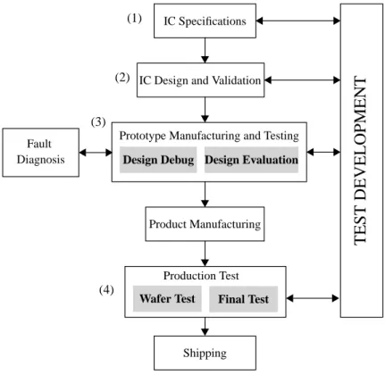
3.2. Test Flow
Test can be carried out during different phases of integrated circuit (IC) design. According to Figure 3-1 [Engi00, Huer93a], the first step in test flow is the IC specifications. At this step, specifications are usually given in terms of transient and steady-state performances. A circuit is designed so that its specifications fulfill the requirements specified by the user.
The second step is the design and its validation. The goal of this step is to ensure that the design obtained as an outcome of the design process is correct.
The third step of the test flow is prototype manufacturing and testing. Prototype testing is pri-marily aimed at verifying the circuit under test (CUT) characterizations and to certify that CUT can be sent to mass production, where an exhaustive test must be applied to identify any fault or any disparity with the required specifications. Therefore, prototype testing is focused on design mistakes rather than on manufacturing defects. Prototype testing consists of two stages: design debug and design evaluation. The design debug ensures that the circuit under test (CUT) performs its intended functions correctly using measurement instruments such as waveform generators and oscilloscopes. For example, in order to ensure that the filter behaves as designed, its frequency response and some transient characteristics such as settling time and rise time need to be tested. The design evaluation is performed by measuring specified perfor-mance specifications under many different conditions such as a range of temperatures and input voltages to evaluate worst-case conditions.
In prototype testing, the main specifications of a CUT are checked. If it does not operate as expected, a diagnostics technique is employed to detect and locate faults responsible for the malfunctioning and to decide whether a circuit requires modifications in circuit design in order to enhance the yield of the IC. As prototype testing is performed on only a small number of ICs, the test time is not a primary limitation. However, the most important factor is the accu-racy of the measurements which requires very expensive automatic test equipment.
After a design is manufactured, the fourth step of test flow, which called production testing, is performed. The target of the production testing is to detect the defects resulting from the imperfections of the manufacturing process. Production testing is performed to make a fail/ pass decision, or to distinguish good circuits from faulty ones. Testing cost (reflected as test time, throughput and the cost of automatic test equipment) is a major concern of production testing. Since packaging and final test are more expensive than all other manufacturing steps, an additional testing stage called wafer test is added before packaging. At the wafer test stage, simple parametric tests e.g. DC and low-frequency AC signals are carried out to detect faulty chips. Faulty naked dies are rejected and fault-free dies are packaged. Then, the final step of CUT testing called the final test is achieved on packaged dies. In the final test, high frequency tests can be applied and a subset of specifications is carefully chosen for measurement. This subset of specifications must guarantee that no faulty chips are shipped. The time spent on production testing can be very long, therefore, the number of applied test stimuli and measure-ments must to be minimized.
After achieving the final test step, the chips are ready for shipping to the end-equipment man-ufacturer.
After shipping the chips, the board where the chip is embedded needs to be tested. Further-more, the chip is tested during the operation in the field. Many faults may occur due to aging or environment conditions. In this case, a fault diagnosis is needed to segregate the faulty chips from the good ones.
Figure 3-1: A general overview of the design and test flow for analog circuits
Figure 3-2: Test Economic IC Specifications
IC Design and Validation
Prototype Manufacturing and Testing
Product Manufacturing Production Test
Shipping
TEST DEVELOPMENT
Wafer Test Final Test Design Debug Design Evaluation
Fault Diagnosis (1) (2) (3) (4)
Wafer Chip Board System Field 0.1 1 10 100 1000 Test Activity Cost
As a rule of thumb, the incremental cost of detecting, locating and repairing a fault through each successive phase of IC development is around ten times higher than the previous phase, as shown in Figure 3-2 [Robe01].
3.3. Fault Classification
Any deviation in the electrical or geometrical properties of the manufactured IC from the val-ues given by the IC layout beyond the expected process variation is called a defect [Engi00]. The effect of a defect on the electrical characteristics of the IC deviating from the specified behavior is called a fault [Engi00].
In other words, a fault is the consequence of a defect, but it is also possible that a circuit with a defect electrically has no fault at all.
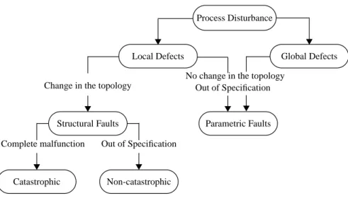
In this section, fault classification of analog circuit faults is given based on [Huer93a, Milo98, Engi00]. The sources of faults in analog circuits (process disturbance) are either global or local defects. Global defects include imperfect parametric control in IC manufacturing, insta-bilities in process conditions, material instainsta-bilities, substrate inhomogeneities and mask mis-alignments. Such defects affect all chips on a wafer in approximately the same way. On the other hand, local defects (such as spot defects, oxide pinholes, missing contact, etc.) are usu-ally originated from particles in the fabrication process and affect individual devices or a very small region on a chip.
Figure 3-5: Classification of analog faults Process Disturbance
Change in the topology
Local Defects Global Defects No change in the topology
Parametric Faults Catastrophic Complete malfunction Non-catastrophic Out of Specification Structural Faults Out of Specification
![Figure 2-1: Analog domain and levels of abstraction [Ashe03]](https://thumb-us.123doks.com/thumbv2/123dok_us/10155147.2917278/15.892.129.766.259.582/figure-analog-domain-levels-abstraction-ashe.webp)
![Figure 3-7: DSP-based testing structure [Mah87]](https://thumb-us.123doks.com/thumbv2/123dok_us/10155147.2917278/47.892.254.638.614.852/figure-dsp-based-testing-structure-mah.webp)