Ultra Low Power Process Tolerant 10T (PT10T) SRAM with Improved Read/Write Ability for Internet of Things (IoT) Applications
Pooran Singh and S. K. Vishvakarma
Nanoscale Devices, VLSI Circuit and System Design Lab
Discipline of Electrical Engineering, Indian Institute of Technology Indore, India Email: [email protected]
Abstract: An ultra-low power (ULP), power gated static random access memory (SRAM) is presented for Internet of Things (IoT) applications, which operates in sub-threshold voltage ranges from 300mV to 500mV. The proposed SRAM has tendency to operate in low supply voltages with high static and dynamic noise margins. The IoT application involves battery enabled low leakage memory architecture in subthreshold regime which has low power consumption. Therefore, to improve power consumption along with better cell stability, a power gated 10T SRAM is presented.The proposed cell uses a power gated p-MOS transistor to reduce the leakage power or static power in standby mode. Moreover, due to the schmitt triggering and read decoupling of 10T SRAM the static and dynamic behavior in read, write and standby mode has shown enhanced tolerance at different process, voltage and temperature (PVT) conditions. The proposed SRAM shows better results in terms of leakage power, read static noise margin (RSNM), write static noise margin (WSNM), write-ability or write trip point (WTP), read-write energy and dynamic read margin (DRM). Further, these parameters are observed at 8-Kilo bit (Kb) and compared with already existing SRAM architectures.It is observed that the leakage power is reduced by 1/81×, 1/75× of the conventional 6T (C6T) SRAM and read decoupled 8T (RD8T) SRAM, respectively at 300mV VDD.On the contrary, RSNM, WSNM, WTP and DRM values are improved by 3×, 2×, 11.11% and 31.8% as compared to C6T SRAM, respectively. Similarly, proposed 10T has 1.48×, 25% and 9.75% better RSNM, WSNM and WTP values as compared to RD8T SRAM, respectively at 300mV VDD.
Keywords: power gating; read decoupling; read-write static noise margin; dynamic noise margin; read-write energy; schmitt trigger; leakage power.
1. Introduction
The massive constrain headed for internet of things (IoT) devices has led to developments of ultra-low power (ULP) systems-on-chip (SoCs) that are capable of operating in sub-threshold voltages [1, 2]. One way to guarantee low power and energy consumption is to scale down the supply voltage to the sub-threshold region [3]. However, the reduced on-to-off current ratio (ION/IOFF) and the exponential dependence of the current on the threshold voltage (Vth) in the sub-threshold region introduces
many challenges especially in rationed circuits such as the traditional 6T static random access memory (SRAM) bit-cell. Since, conventional non-volatile memories consume higher read and write power, the scaling of supply voltages and the techniques to reduce leakage at sub-threshold voltages needed. However, the low cell stability is also one of the factor which defy conventional SRAM architecture to not to work at sub-threshold region [4].
However, due to rapid growth of internet market through all over the world, Internet of Things (IoT) brings connectivity, communication, and data gathering to existing devices. IoT includes countless devices connected and communicated with each other to enrich the present lifestyle, and its applicability ranges widely from traditional internet to industrial internet and also to consumer internet [5]. Independent of its application, there is always one common trait: the need of on chip memory that drives the connected world by enabling the capture, transmission, analysis and storage of the data up and down to power the IoT. In addition, IoT applications in which portable devices communicate with each other and thus require an enormous amount of memory to store and process data. The memory used in IoT can differ with the need of applications related to market. For instance, in case of huge amount of data storage and handling information for a long period of time and where the data usage is not much frequent, a high density memory like DRAM and Flash are used. In case of high data transfer rate systems, a fast SRAM memory is required, where a high clock frequency is required to communicate between IoT devices. Therefore, SRAM is always preferred to be used as cache memory due to its faster response. Moreover, the robustness of such memory systems, for the variations in environmental conditions and power efficiency are two of the most important design constraints [4]. As per the literature, more than 40% of the active energy is consumed due to the leakage currents in modern high performance processors [6, 7]. Also, most of the time a large number of SRAM cells used in today’s on-chip cache memory stay in the standby mode where leakage power dominants over the dynamic power. Thus, leakage reduction has become the imperative concern in the SRAM memory design.
Implementation of ULP SRAM is also has a significant purpose in embedded systems such as biomedical implants, self-powered wireless sensors, and battery enabled portable electronic devices in which battery life or input power is a main concern [8]-[11]. Simultaneously, cell stability is also considered as one of the major concerns in SRAM architectures. It is observed that for standard 6T SRAM cell, read static noise margin (RSNM) is vulnerable at subthreshold regions, while reading through full swing sense amplifier (SA) [12]-[15]. It is well known that the best way to reduce the power in a digital circuit is to lower the supply voltage as it has a direct impact on the power consumption [16]-[20]. SRAM design remains challenging and becomes more interesting due to the rapid advancement of CMOS technologies and with increased demand of on-chip memory in the wireless implantable and wearable biomedical sensors. Subsequently, the SRAM memory contributes as the major source of power consumption in an electronic device due to introduction of leakage in subthreshold region. Emerging memory technologies are continuing to make steady progress towards product intercepts, including phase change random access memory (PCRAM) and
resistive RAM (ReRAM). However, embedded SRAM continues to be a critical technology enabler for a wide range of applications from high-performance computing, graphics for mobile applications, wearable electronics and internet of things (IoT) applications [21]. Nevertheless, the vigorous scaling of process technologies driven by Moore’s law resulted in statistical process variations in the transistor parameters such as threshold voltage (Vth), channel length (L), and mobility [22]. Therefore, device
variability in modern processes has become a major concern in SRAM design, degrading performance, bit density, power, yield, and reliability. Other challenges for SRAM include VDDmin, leakage and dynamic power reduction. However, stability has long
been a major concern for SRAM architectures. Low voltage operation and increased process variation caused by random dopant fluctuation (RDF) & line edge roughness (LER) have been shown to degrade the stability and performance of SRAM, and may lead to functional failure [23]. Aggressive power reduction can be achieved by subthreshold operation. However, operation at these reduced voltages degrades robustness, due to depleted noise margins and higher susceptibility to process variations and device mismatch. However, substantial amount of research has so far been reported regarding noise margin improvement, including RSNM, WSNM, HSNM, data retention and yield improvement of SRAM [24-26], like P-P-N based 10T SRAM [27], decoupled latch [28], [29] and 5T SRAM cell [30]. Some popular methods include voltage scaling, switching activity reduction, architectural techniques, and device sizing and new device structures [31-33]. All these works analyze and quantify the impact on cell stability degradation in lifetime circuit performance.
In order to achieve high RSNM, a basic and effective way is the decoupling of a storage node from the bit-lines during read operation [28]. Kim. et al. [34] introduced a new 8T SRAM cell that can operate up to 200mV by utilizing the reverse short channel effect (RSCE). The operation of standard 6T and standard 8T SRAM at subthreshold voltage is unachievable, primarily due to the degraded static noise margins (SNMs) and extreme fluctuations in the device currents under process variations. Therefore, the work in [30] presents a robust, low-voltage SRAM bit cell with a reduced transistor count, as compared to the standard 6T. Multi-threshold devices are also used to achieve better noise margins. To further improve cell functionality, the pull-up PMOS devices are implemented with high voltage threshold (HVT) devices. In [35], cell breaks the feedback loop of the cell during the read operation to guarantee the stability of stored data. In [36], a suitable read operation is provided by suppressing the drain-induced barrier lowering (DIBL) effect and controlling the body-source voltage dynamically. Proper usage of low-threshold voltage transistors in the SRAM design helps to reduce the read access time and enhance the reliability in the subthreshold region. Due to superior gate control, improved electrostatic integrity and variability, FinFET have demonstrated satisfactory scalability and feasibility for mass production of post 22nm node. Thus, FinFET is an ideal alternative to planar CMOS in SRAM designs [37], [38]. However, while considering bulk-CMOS SRAM, the need of diminution in leakage power at subthreshold region has still a primary challenge. Due to continuous device scaling and reduction in supply voltage the leakage power value has come out as equal as dynamic power. Though, some of the above mentioned works on bulk-CMOS SRAMs has considered vital for power reduction, but it degrades noise margins and read-write speed. The same has appeared with some existing works, which has significant improvement in the noise margin and read-write speed but at the same time the overall power has increased. To overcome the tradeoff between power, delay and noise margin we have proposed a feedback controlled 10T SRAM which improves the SNM, speed as well as total power consumption at the same time.
To overcome the process intolerance occurred due variations in various process parameters like channel length, gate-oxide, DIBL etc. and the variability in device due to noise occurred from temperature variations for IoT applications a differential process tolerant 10T SRAM cell is proposed in this paper. The rest of the paper is organized as follows: Related work and motivation are detailed in section II. Proposed 10T SRAM architecture with 64×128 array (8-Kb) is presented in section III. Operations and working of 8KB SRAM is explained in section IV. The simulation results and discussion of proposed 10T SRAM is mentioned in section V. Lastly, section VIII concludes our work.
2. Related Work and Motivation
Q
QB
MN1 MN3
MP1 MP2
MN2 MN4
MN7 MN5
BL BLB
WWL WWL
MN6 MN8
RWL RWL
(a) (b) (c)
WWL
MN7
BL BLB
Q
QB
MN1 MN3
MP1 MP2
MN2 MN4
RWL XOR
WWL WWL
MN5 MN6
MN8
GND GND
Process Tolerant 10T (PT10T)
SRAM cell WWL
RWL
MN_GND XNOR
BL BLB
Q
QB
MN1 MN3
MP1 MP2
MN2 MN4
MN7
VVDD
WWL WWL
VDD
MN5
MN6 MN8
RWL
MP_VDD
(d) (e)
Figure 1. (a) Architecture of convetional (C)-6T SRAM cell. (b) Architecture of read decoupled (RD)-8T SRAM cell. (c) Structural design of schmitt trigger (ST)10T SRAM cell [39]. (d) Schematic of low power (LP10T) SRAM cell [44]. (e) Schematic of proposed process tolerent 10T (PT10T) SRAM cell.
3. Architecture of 10T SRAM Cell
Technological advances and cost reduction have resulted in remarkable development of computing devices. If continued, this trend might result in tens of billions of computing systems consisting of personal computers, desktop machines, smartphones, wearables and many units connected to the internet; collectively known as the Internet of Things (IoT). This dramatic growth in compute devices results in a data explosion and would require millions of Zettabytes of memory in order to perform this large scale of computing. Thus, memories play a critical role in future energy efficient computing systems and considering the points, a subthreshold, low leakage power with high stability SRAM is presented in this section.
The proposed cell has two write access n-MOS transistors, MN1 and MN3 and two read access transistor MN2 and MN4. The BL contains single bit information to write and at the same time BLB contains the complementary of that. In addition, n-MOS transistors MN2 and MN4 which are connected with virtual ground n-MOS transistor MN_GND are used as a read path. The BL and BLB are precharged to VDD before the read operation is performed. The MP1-MP2-MN5-MN6-MN7-MN8 transistors form a latch, where, MP1 and MP2 are the pull-up transistors linked to virtual VDD (VVDD). In addition, MN5 to MN8 forms Schmitt triggered logic, which eventually enhances the read noise margin [39]. Furthermore, two transistors MP_VDD and MN_GND are shared with each row of 8-Kb SRAM as shown in Fig. 3, where, MP_VDD is used as a power gating p-MOS transistor, which disconnects the path between VDD and GND at hold state to improve the leakage power. On the other hand, the MN_GND is used as a virtual ground path to read information from the cell.
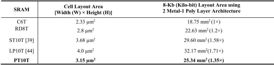
Table I Comparison of cell layout area at 65nm standard CMOS technology
SRAM cell Numbers of low voltage threshold (LVT) transistors used Layout Area [Width (W) × Height (H)]
C6T 6 (2 LVT p-MOS, 4 LVT n-MOS) 1× (2.33µm×1µm=2.33µm2)
RD8T 8 (2 LVT p-MOS, 6 LVT n-MOS) 1.2× (2.33µm ×1.2µm=2.8µm2)
ST10T [39] 10 (2 LVT p-MOS, 8 LVT n-MOS) 1.58× (2.52µm ×1.46µm=3.68µm2)
LP10T [44] 10 (2 LVT p-MOS, 8 LVT n-MOS) 1.71× (2.8µm ×1.46µm=4µm2)
Table II Logic Truth table for various operations in proposed PT10T SRAM
Operation WWL RWL BL BLB
Write 1 1 0 1 0
Write 0 1 0 0 1
Read 1 0 1 Discharging 1
Read 0 0 1 1 Discharging
Hold 0 0 1 1
WWL BL
RWL WWL BLB
Q
QB RBL
GND VDD
VDD
GND 2.33µm
1.2µm
M3
M5 M2
M1
M6
M4
M7 M5 All W=150nm, L=60nm
RWL
WWL
GND BL
VDD
VDD
BLB GND
WWL
RWL Q
QB MP1
MP2 MN2
MN1
MN5
MN6
MN8
MN4 MN3 MN7
2.52µm
1.
4
6
µ
m
(a) (b)
2.8µm
1.
46
µ
m
2.16µm
1
.46µ
m
(c) (d)
Figure 2. The layout of various SRAM architecture at W=150nm and L=60nm at 65nm Standard CMOS Technology. (a) Layout of convetional RD-8T SRAM cell. (b) Layout of schimtt trigger 10T SRAM cell [39]. (c) Layout of low power 10T (LP10T) SRAM cell [44]. (d) Layout of proposed process tolerent 10T (PT10T) SRAM cell.
4. 10T SRAM Cell Based 8kb Marcoblock and Area Overhead
To observe the area overhead and to have a better view towards the functionality and placing of SRAM cell and various controlling blocks at array level a simplified architecture of 10T SRAM array is portrayed in Fig. 3. In addition, the functioning of 10T SRAM is explained in Table II. The table shows the truth table of various operations takes place in the proposed SRAM architecture. The SRAM array uses internal inputs derived from RWL and WWL signal to control the power gated p-MOS transistor. However, the proposed SRAM array in Fig. 3 shows the complete correlation of various controlling signals and demonstrates how single bit information is written and read using a high speed differential current compensation sense amplifier (DCC-SA) [45-47]. The layout area of different SRAM architectures is shown in Fig. 2 and the comparison between cell areas is mentioned in Table I. It shows that the proposed SRAM has 17% and 27% reduction in footprint area as compared to ST10T [39] and LP10T [44] SRAM, respectively.
10T 10T
Shared WWL Shared Virtual VDD
Shared VGND
Shared RWL
PRESA
BLB
PRESA
OUT OUTB
M2 M0 M1 M3
M4 M5
M6 M7
M8 M11 M9
M12 M10
BL
SO SOB
SEN BL BLB
BLB
10T 10T
10T 10T
10T 10T
PRESA
BLB
PRESA
OUT OUTB
M2 M0 M1 M3
M4 M5
M6 M7
M8 M11 M9
M12 M10
BL
SO SOB
SEN BL BLB
BLB
10T 10T
DCC Sense Amplifier []
Shared Virtual VDD
RWL RWL WWL
Shared VGND
Figure 3. Simplified array acrchitecure of 10T SRAM, where read is perforemed using high speed differentail current compensation sense amplifier (DCC-SA) [45].
using MP_VDD) and read static noise margin (RSNM), dynamic read margin (DRM) using MN_GND. A XNOR gate is also introduced at each row of the SRAM Macro to provide a sleep input to the power gated p-MOS transistor MP_VDD. The XNOR gate has 4 MOS transistor (2 n-MOS and 2 p-MOS) integrated at each row of the array. These extra transistors bear a channel width of 2µm which is 13.33× more than that of the SRAM MOS transistors width (150nm). Consequently, including all overhead and SRAM cell layout area, we observed a total footprint area of 8-Kb SRAM array of C6T, RD8T LP10T, ST10T and proposed SRAM cell as shown in Table III. From the table it observed that the proposed cell has 35% and 12.5% higher Macro area as compared to C6T and RD8T, respectively. On the other hand, the proposed 10T SRAM has 17% and 27% lesser Macro area as compared to ST10T and LP10T, respectively.
SEN
PC PC PC PC
WBL WBBL
WE
REB REB
BL
BLB RBBL RBL
WBL WBBL
WE
REB REB
BL
BLB RBBL RBL
PRESA
BLB
PRESA
OUT OUTB
M2 M0 M1 M3
M4 M5
M6 M7
M8
M11 M9
M12 M10
BL
SO
SOB
SEN
BL BLB
Table III Comparison of 8-Kb layout area at 65nm standard CMOS technology
SRAM [Width (W) × Height (H)] Cell Layout Area 2 Metal-1 Poly Layer Architecture 8-Kb (Kilo-bit) Layout Area using
C6T 2.33 µm2 18.75 mm2 (1×)
RD8T 2.8 µm2 22.63 mm2 (1.2×)
ST10T [39] 3.68 µm2 29.60 mm2 (1.58×)
LP10T [44] 4.0 µm2 32.17 mm2(1.71×)
PT10T 3.15 µm2 25.34 mm2 (1.35×)
5. Operations and Working of 10T SRAM Using Differntial Current Compentation - Sense Amplifier (DCC-SA) A. Read operation
Before reading the information, BL and BLB are precharged to VDD using the precharge logic input PC as shown in Fig. 3.The read operation is obtained through ultra fast differential current compensation sense amplifier (DCC-SA) [38-40]. The read operation is performed by keeping read word line (RWL) to HIGH and write word line (WWL) to LOWand XNOR_I/P kept at LOW value. Since, for read ‘1’ (Q=1), logic 1 is stored at the storage node Q and RWL is kept HIGH, which eventually turns ON MN_GND and MN2. This forms a discharging path across BL-MN2-MN_GND and a voltage difference, ΔVBL= {(VDD (VBLB
)-(VDD-Iread, BL×RMN2-GND)} appears between BL and BLB line which is sensed by the full swing inverter sense amplifier [45-47].
Where, Iread is the cell current and RMN2-GND is the resistance through MN2 and MN_GND. The read access time is measured as the
time the RWL signal is activated until the BLB is discharged to minimum required potential needed by SA to read. The sensing voltage ΔVBL required for DCC-SA [45-47] here is ranges between 50mV-80mV. The read access time and power is measured
across a 64-bit column of the SRAM cell. The parasitic capacitance of SRAM column is measured after RC-extraction in Cadence layout design at 65nm UMC Technology. The read operation of proposed cell is shown in Fig. 4(a). The sense amplifier works well in subthreshold or near threshold voltages ranging from 0.3V to 0.7V. The circuit topology of DCC-SA is shown in Fig. 5(a) and the simulated transient voltage at 0.7V VDD is shown in Fig. 5(b). Fig. 5(b) shows the working of SA, as the SEN and RWL is activated and chip select (CS) is HIGH, the SA detects the voltage difference (sensing voltage) between BL and BLB. As soon as, the voltage difference reaches to range of sensing voltage, the output node SOB gets logic HIGH, which redirects that logic ‘1’ stored at storage node Q of the SRAM.
B. DCC-SA architecture and operation
Fig. 5(a) illustrates the detailed schematic of differential-current-compensation based SA (DCC-SA) [45-47], which is capable of overcoming sensing device Vthmismatch effect on SA differential current. Differential current is defined as |IL-IR|. Here ILand
IRare current in the left and right branch of SA. The SA approach differs significantly from other approaches, which use different
MOS devices for compensation/calibration of offset, resulting in increased vulnerability to mismatch between devices. In Fig. 5(a) transistors M0-M8 configured the DCC-SA. The body terminals of NMOS M4 and M5 in latch are connected to decoupled bitline (DL) and decoupled bitline bar (DLB), respectively. Before sensing, SA pre-charge signal (PRESA) will be at logic LOW to ensure that the nodes SO and SOB are pre-charged at VDD. Since DLs are also pre-charged, it results in equal body bias of transistors M4 and M5. A read access starts by the activation of word line (RWL in our case) signal. This generates the differential voltage at BLs which results in different body bias voltage for M4 and M5 devices. Thus for read ‘1’ case before the activation of SEN signal the body of the left NMOS M4 will be at higher potential than the body of NMOS M5, this resulted in IDS(M4) >
IDS(M5). In case of no offset in sensing devices, this will results in correct sensing. However in case of offset (Vth (M4) >Vth (M5))
this compensates the current in the corresponding branch. Thus, at the beginning, the transistor with a lower Vthsources a larger
current, which eventually creates a high current in corresponding branch is compensated because of the higher body voltage for a smaller threshold voltage. In other words, before SEN activation, a differential voltage is developed between the bit-lines which compensates the threshold voltage difference of M4 and M5 to achieve higher effective current in corresponding branch. Thus the device with higher body bias has lower Vth. This helps in dynamically adjusting the overdrive potential of this device and
GND GND
Process Tolerant 10T (PT10T)
SRAM cell WWL=0
RWL=1
MN_GND XNOR_OUT=0
BL=VDD- (Iread×RMN2-MN_GND) BLB=VDD
Q=1
QB=0
MN1 MN3
MP1 MP2
MN2 MN4
MN7
VVDD
WWL=0 WWL=0
VDD
MN5
MN6 MN8
RWL=1
MP_VDD
Iread
GND GND Process Tolerant
10T (PT10T) SRAM cell WWL=0
RWL=1
MN_GND XNOR_OUT=0
BL=VDD BLB=0
Q=1
QB=0
MN1 MN3
MP1 MP2
MN2 MN4
MN7 VVDD
WWL=0 WWL=0
VDD
MN5
MN6 MN8
RWL=1
MP_VDD
Iread
(a) (b)
Figure 4 (a) State of read ‘1’ operation in proposed 10T SRAM. (b) State of write ‘1’ operation in proposed 10T SRAM. The power gated PMOS is turned ON for read-write operation.
C. Write operation
For write operation, WWL must be kept HIGH and RWL is at LOW. However, by making WWL (HIGH) and RWL (LOW); XNOR_OUT is switched to LOW value.The logic 1 is written to storage node Q through BL-MN1-Q as shown in Fig. 4(b). However, the write ‘1’ access time is measured as the time when WWL signal is activated and reaches to its VDD/2 value and storage node Q reaches to 90% of VDD value.Similarly, write ‘0’ time is measured as the time when WWL signal is activated and reaches to its VDD/2 and storage node Q reaches to 10% of VDD. The half select issue in write operation is also taken care of by putting a WE signal at each column of SRAM array as shown in Fig. 3. By making read and write path separate using WE and REB the sensing and writing operations are separated which eventually helps to negate the half select read and write issue.
D. Data Retention
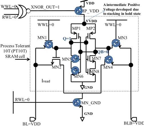
Generally, the memory cell remains in static or hold state at most of time. Therefore, there would be very high possibility of increase in leakage power in SRAM cell in different PVT conditions. In proposed PT10T SRAM, the control signal XNOR_OUT
(a) (b)
GND GND
Process Tolerant 10T (PT10T)
SRAM cell WWL=0
RWL=0
MN_GND XNOR_OUT=1
BL=VDD BLB=VDD
Q=1
QB=0
MN1 MN3
MP1 MP2
MN2 MN4
MN7
VVDD
WWL =0 WWL =0
VDD
MN5
MN6 MN8
RWL=0
MP_VDD
Iread
A intermediate Positive Voltage developed due to stacking in hold state
Figure 6. Architecture/Schematic of proposed 10T SRAM cell at hold mode.
turns OFF MP_VDD which helps to reduce the leakage current by disconnecting the path of the latch from VDD to GND. The leakage power in C6T SRAM cell introduces due to non-availability of virtual VDD transistor such as MP_VDD.The standby or leakage power dissipation is one of the major problems with embedded cache in sub-nanometer technology nodes. Leakage power is the major contributor to the total power consumption of SRAM, as most of the cells remain in the idle state. The leakage current has mainly three components, i.e. Gate leakage, Junction leakage and subthreshold leakage through different transistors [48]. If two devices are connected in series, then they form a stack and if one terminal of a stack is connected to VDD and the other end is connected to ground, and then the intermediate node rises to certain value, which is higher than the ground potential. In proposed SRAM at hold mode, the master transistor (MP_VDD) is turned OFF as output of the XNOR-gate is HIGH (due to both WWL and RWL are LOW). Therefore, the cross-coupled inverters are decoupled from the VDD and a stack is formed between MP1, MP2 and MP_VDD. Because of this effect, the intermediate node VVDD rises to some positive voltage [49]. This positive voltage reduces leakage and hold power during standby mode. However, in C6T and RD8T SRAM cells, there is a potential difference of VDD in-between VVDD and GND terminal. But due to the power gating of VDD the virtual node VVDD now set at a positive voltage VVDD lower than VDD, which eventually reduces the hold static noise margin (HSNM) but improves the leakage power at ultra-low power applications.
6. Simulation Results of PT10T SRAM
The proposed 10T SRAM is simulated in 65nm standard CMOS technology. Post layout simulation at 6-sigma (σ) process variations are observed and compared with C6T, RD8T, ST10T [39] and LP10T [44] SRAMs to determine various constraints like leakage power, read-write delay and power, power delay product (PDP), read static noise margin (RSNM), dynamic read margin (DRM), write static noise margin (WSNM) and write trip point (WTP). Further, all the listed constraints are observed at different temperature values ranging from 0˚C to 100˚C and at different process corners namely fast-fast (FF), slow-slow (SS), typical-typical (TT), slow-fast (SF) and fast-slow (FS) using 1000 Monte Carlo (MC) simulations
A. Simulation Setup
The simulation setup is observed through Monte Carlo post layout simulations on an 8Kb SRAM array. The read-write access time and power is measured by applying a write and read operation at single column of the array. The proposed SRAM macro has 64-bit column coupled with a DCC-SA. The DCC-SA is used as a sense amplifier which takes a small differential positive sensing voltage as an input and attains an output which is equivalent to the stored information in the SRAM cell. To read and write a read and write access transistor used to separate the read and write path. The row and column decoder are used to activate the WWL and RWL of the Marco. The setup for all operations is observed at the worst case process corner. The write and read operation are taken from BL and BLB of the SRAM. While reading the information from the SRAM the bit-lines are pre-charged to VDD using pre-charge (PC) signal. Further, all the observations are taken using 1000 Monte Carlo simulations.
B. Write and Read Analysis
as compared to C6T, RD8T, LP10T [44] and LP9T [43] SRAM, respectively at 300mV supply voltage. The outcome achieved illustrates an enhancement in dynamic write ‘0’ power by 5.2%, 1%, 10% and 6.6% as compared to C6T, RD8T, LP10T [44] and LP9T [43] SRAM, respectively at 300mV supply voltage.
0.2 0.3 0.4 0.5
0 300 600 900 1200 1500 1800 2100
0.299 0.300 0.301 100 150 200 250 300 Wri
te '1' D
el a y (n s) VDD (V) C6T RD8T LP10T LP9T P10T Write 1 delay at
Worst Case process corner (SS)
W rit e ' 1 ' del ay (n s) VDD (V)
0.2 0.3 0.4 0.5
0 200 400 600 800 1000 1200 1400
0.299 0.300 0.301 50
100 150
Write 0 delay at Worst Case process corner (SS)
C6T RD8T LP10T LP9T P10T
Write '0' D
el ay (ns) VDD (V) W ri te '1 ' D e lay ( ns) VDD (V)
(a) (b)
Figure 7. (a) Write ‘1’ delay, (b) Write ‘0’ delay at slow-slow (SS) Process corner.
0.2 0.3 0.4 0.5 500 1000 1500 2000 2500 W rit
e '0' P
ow er (nW ) C6T RD8T LP10T LP9T P10T VDD (V)
FF Pr oces
s Corn er (P
C) 0.2 0.3 0.4 0.5 0 1000 2000 3000 4000 5000 6000 C6T RD8T LP10T LP9T P10T
Write 1 Power (
nW)
VD
D (V) FF Pr
oces s Corn
er
(a) (b)
Figure 8. (a) Write ‘0’ power, (b) Write ‘1’ power at fast-fast (FF) Process corner.
0.20 0.25 0.30 0.35 0.40 0.45 0.50
0.03 0.06 0.09 0.12 0.15 0.18
0.21 C6T
RD8T LP10T LP9T P10T
W
riite '0' Energy
(fJ
) at
SS PC
VDD (V)
SS Process Corner (PC)
0.2 0.3 0.4 0.5
0.05 0.10 0.15 0.20 0.25
0.30 C6T
RD8T LP10T LP9T P10T En er g y Wr ite ' 0' ( fJ ) at F F PC VDD (V)
Write '0' Energy at FF Process Corner (PC)
(a) (b)
0.2 0.3 0.4 0.5
0.03 0.06 0.09 0.12 0.15 0.18 0.21 0.24
0.27 C6T
RD8T LP10T LP9T P10T Wri te '1 ' En erg y (fJ) VDD (V)
SS Process Corner
0.2 0.3 0.4 0.5
0.05 0.10 0.15 0.20 0.25 0.30
0.35 C6T
RD8T LP10T LP9T P10T Wr ite 1 En er gy ( fJ) VDD (V)
FF Process Corner
(c) (d)
0.0 20.0µ 40.0µ 60.0µ 80.0µ 100.0µ 0.0
0.2 0.4 0.6 0.8 1.0
BL
Voltage (V)
Read Access Time (S)
SEN BLB BL RE
RWL Read 1 delay observed at 32-bit Column = 20μS RWL, SEN, RE
BLB, BL Precharged at 200mV
BLB
0.2 0.3 0.4 0.5
0 1x10⁴ 2x10⁴ 3x10⁴ 4x10⁴
R
ead
Access Ti
me (ns)
VDD (V)
C6T LP10T ST10T PT10T
Read Delay Observed at different supply voltages at SS process corner
Read delay at 300mV VDD shows proposed cell has faster read operation as compared to C6T and ST10T
(a) (b)
0.2 0.3 0.4 0.5
10 12 14 16 18 20 22 24 26
Read Energy
(fJ)
VDD (V)
C6T
LP10T
P10T
Read Energy observed at SS Process Corner
(c)
Figure 10. (a) State of input variables in read operation where micron (µ) is 10-6, (b) Read access time at SS process corner at
different supply voltages and (c) Read energy premeditated at different supply voltages.
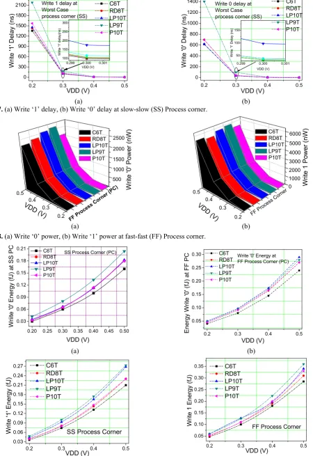
Further, Fig. 9 shows the energy consumption of various SRAM cells at different supply voltages at SS and FF process corner in write ‘0’ and write ‘1’ operation.The results obtained show an improvement in write ‘1’ energy by 1.23%, 14% and 20% as compared to RD8T, LP10T and LP9T SRAM, respectively at 300mV supply voltage. However, write‘0’ energy is improved by 1%, 6.2% and 5.2% as compared to RD8T, LP10T and LP9T SRAM, respectively at 300mV supply voltage. Furthermore, the read delay is measured when RWL is activated and precharged bit-lines discharges and reaches to the minimum sensing voltage required by SA [38-40]. In our proposed DCC-SA architecture [45-47], by estimating the read sensing voltage at worst case process corner, we examined a differential voltage of range 50mV-80mV required for generating an output signal to read data from SRAM. Fig 10(a) shows the simulation states of SRAM at read time. The proposed SRAM fast read access as compared to the existing SRAM cells as stated in Fig 10(b). However, the power measured until the time, where the difference of bitline voltage reaches to the sensing voltage is defined as a read power. Fig. 10(c) illustrates the plot of read energy and it can be observed that proposed SRAM have less energy consumption as compared to C6T and LP10T SRAM cells.The read access time of proposed SRAM is 1.6×, 1.57× better than that of C6T and ST10T [39] SRAM in SS process corner at 300mV VDD. In addition, the read energy of proposed cell is 4% and 3% better than C6T and LP10T SRAM in SS process corner at 300mV VDD. C. Standby or Leakage power
0.2 0.3 0.4 0.5 0 5 10 15 20 25
0.299 0.300 0.301 0.01 0.1 1 Lea ka ge Po w er (n W ) VDD (V) Leakage Power
measured in Log scale C6T
RD8T LP10T LP9T P10T
Leakag
e Power (nW)
VDD (V) 0.0 100.0p 200.0p 300.0p 400.0p
0 100 200 300 400 500 600 700 800 900 1000 Occuran ces
Leakage Power (W) 500mV 400mV 300mV 200mV Leakage Power in
pico-watts (pW) or 10-12 W
measured at different supply voltages
(a) (b)
Figure 11. (a) Leakage power at different supply voltages. (b) Distribution of leakage power of proposed SRAM at various supply voltages, where Pico (p) is 10-12 of unit.
0.0 2.0n 4.0n 6.0n 8.0n 10.0n
0 100 200 300 400 500 600 700 800 720 660 720 800
A distribution curve of leakage power shows its window spread
from 0 to 10 nW (10-9 Watt) power
at 300mV VDD at different temp
Occur
re
n
ces
Leakage Power (W)
0 °C 25 °C 50 °C 75 °C 100 °C
C6T SRAM 850
0.0 2.0n 4.0n 6.0n 8.0n 10.0n 12.0n 14.0n
0 100 200 300 400 500 600 700 800 900 745 800
850 A distribution curve of leakage
power shows its window spread from 0 to 10 nW (10-9 Watt) power at 300mV VDD at different temp values O c cu rr en ce s
Leakage Power (W) 0°C 25°C 50°C 75°C 100°C
RD8T SRAM
890
0 20p 40p 60p 80p 100p 120p 140p
0 100 200 300 400 500 600 700 800 Occur rences
Leakage Power (W)
0°C
25°C
50°C
75°C
100°C
Leakage Power of proposed 10T SRAM at different temprature values
Peak of distribution curves are
at ≅10pW at 300mV VDD
(a) (b) (c)
Figure 12. (a) Distribution curves of leakage power of 6T SRAM. (b) Distribution curves of leakage power of RD8T SRAM at various temperature values at 300mV VDD. (c) Distribution curves of leakage power of proposed 10T SRAM at various temperature values at 300mV VDD. Where, Nano (n) is defined as 10-9 of unit and Pico (p) is 10-12 of unit.
D. RSNM and read margin
Read static noise margin (RSNM) is measured by applying a DC noise voltage source at one of the storage node Q or QB and investigating the effect on other storage node. The RSNM is examined in the read operation when RWL is HIGH and WWL is LOW. The decoupled read path through BL-MN2-MN_GND doesn’t affects the storage nodes of the SRAM cell, which would further help to neglect the consequences of static noise and as a result, improves the RSNM.The RSNM of the proposed PT10T SRAM cell comes out to be 107mV, which has 3×, 1.48× and 1.48× improved values as compared to than C6T, RD8T and LP10T SRAM, respectively at 300mV VDD as shown in Fig. 13. Consequently, read margin is measured in a situation where there is no static DC noise hampered the storage nodes. While measuring read margin, the RWL is activated HIGH and WWL is kept at LOW. The read dynamic noise margin (RDNM) is observed when the bitline reaches to the sensing voltage. Simultaneously, the voltage difference between storage node Q and QB is definedasRDNM.In our case the RDNM value comes out to be equivalent to 290mV which is 7.5% better than C6T SRAM as shown in Fig. 14(a) and Fig. 14(b) at 300mV VDD.
QB P10T C6T LP10T LP9T RD8T
0.0 0.1 0.2 0.3
0.0 0.1 0.2 0.3
RSNM of C6T =36mV RSNMof LP10T, LP9T and RD8T =72.3mV
Q(V)
QB(V)
RSNM of P10T =107mV
VTC for RSNM
0 20n 40n 60n 80n 100n 0.00 0.05 0.10 0.15 0.20 0.25 0.30 Vol tage ( V )
Read Access Time (s)
QB BLB WL Q RDNM=270 mV C6T SRAM Offset Voltage@50mV required for sense amplifier
0 20n 40n 60n 80n 100n
0.00 0.05 0.10 0.15 0.20 0.25 0.30 Vo lt a g e ( V )
Read Access Time (s)
BLB QB Q RWL
RDNM= 290 mV
P10T SRAM
(a) (b)
Figure 14. (a) RDNM of C6T SRAM and (b) RDNM of proposed PT10T SRAM at 300mV VDD.
0.00 0.05 0.10 0.15 0.20 0.25 0.30 0 100 200 300 400 500 600 Occu rren ce s VDD (V)
Read Margin 6T Read Margin P10T
600
450
6T Read Margin Mean= 265mV
P10T Read Margin Mean=285mV
0.0 0.1 0.2 0.3
0.0 0.1 0.2 0.3 Q(V ) QB(V) Vth+10mV Vth+20mV Vth+30mV Vth+40mV
RSNM at different threshold voltages at VDD=300mV in worst process corner FS
RSNM=75mV
(a) (b)
Figure 15. (a) Distribution curves of RDNM of C6T and PT10T SRAM. (b) RSNM of proposed 10T SRAM at different threshold value of MN5 and MN6 at
300mV VDD.
In addition, In Fig. 15(a), the RDNM distribution curve is plotted using 1,000 Monte Carlo simulations which show that the proposed cell has an average dynamic read margin of 285mV which is 7.5% better than C6T (265mV) at 300mV. Further, in Fig. 15(b), the RSNM value is also observed at different threshold values. The threshold values of the pull down NMOS transistors MN5 and MN6 are varied and the value of RSNM experiential as 75mV at worst case process corner i.e., slow-fast (SF).
E. WSNM and Write Trip Point (WTP)
The write static noise margin (WSNM) is measured at the time of write operation by initiating a linear DC noise at one of the storage nodes and observing the effect of the noise at the other end.The WWL is kept HIGH, the RWL is LOW. The plots in Fig. 16(a), Fig. 16(b), Fig. 17(a) and Fig. 17(b) determines the WSNM of C6T, LP9T, LP10T and PT10T SRAMs at worst case (SF) process corner. Besides, from Fig. 16(a) and 16(b), it is observed that the WSNM of C6T and LP9T SRAM has fail to write at 200mV and the WSNM is 20mV at 300mV VDD which is less than the thermal voltage (∼28mV), and therefore it not good practice to operate at 300 mV VDD. However, the LP10T has a WSNM value of 10mV at 200mV VDD and 30mV at 300mV VDD, consequently it fails to work at 200mV and has near threshold value at 300mV (WSNM=30mV). Therefore, it is suggested to operate LP10T SRAM above 300mV supply voltage. Furthermore, the proposed 10T SRAM has a WSNM value of 21mV at 200mV VDD and 40mV at 300mV VDD, which shows that PT10T can’t able to operate at 200mV VDD, but can work at 300mV VDD. It also shows 2×, 2× and 1.5× better WSNM values as compared to C6T, LP9T and LP10T SRAM at 300mV VDD, respectively.
0.0 0.1 0.2 0.3 0.4 0.5 0.0 0.1 0.2 0.3 0.4 0.5 Q( V) QB(V) 200mV 300mV 400mV 500mV WSNM=20mV<28mV Fails to write WSNM of C6T SRAM measured at Worst Case Process Corner (SF)Fails at 200mV and 300mV VDD
0.0 0.1 0.2 0.3 0.4 0.5
0.0 0.1 0.2 0.3 0.4 0.5 Q( V ) QB(V) 500mV 400mV 300mV 200mV WSNM=20mV< 28mV Fails to write at 300mV VDD
LP9T Fails to write at 200mV and 300mV WSNM of LP9T SRAM measured at SF Process corner
(a) (b)
V (mV)
V (mV)
0.0 0.1 0.2 0.3 0.4 0.5
0.0 0.1 0.2 0.3 0.4 0.5
Q(V
)
QB(V)
200mV 300mV 400mV 500mV
WSNM=10mV <28mV Fails to write at 200mV
WSNM=30mV at 300mV VDD LP10T SRAM Fails to write at 200mV WSNM of LP10T
0.0 0.1 0.2 0.3
0.0 0.1 0.2 0.3
Q(V
)
QB(V)
200mV 300mV QB
WSNM=21mV<28mV Fails to write at 200mV
WSNM of P10T measured at SF Process Corner and it fails at 200mV VDD
WSNM=40mV at 300mV VDD
(a) (b)
Figure 17. WSNM (a) LP10T SRAM and (b) Proposed PT10T SRAM at different supply voltages in worst case slow-fast (SF) process corner.
0.0 0.1 0.2 0.3 0.4 0.5
0.0 0.1 0.2 0.3 0.4 0.5
Voltage 'Q' (V)
Voltage 'QB' (V)
500mV 400mV 300mV 200mV
WTP=20mV<28mV at 300mV VDD Hence Fails to write WTP of C6T measure
at SF Process Corner
0.00 0.05 0.10 0.15 0.20 0.25 0.30
0.00 0.05 0.10 0.15 0.20 0.25 0.30
Vo
ltage
(
V
)
Voltage (V) WTP Mean Value=
VDD - Point of Crossover= 95mV
WTP of proposed 10T measure at 300mV in SF Process Corner
0.2 0.3 0.4 0.5
60 80 100 120 140
160 C6T
RD8T LP10T LP9T P10T
WTP Voltag
e (mV)
VDD (V)
WTP at TT Process Corner
(a) (b) (c)
Figure 18. (a) WTP measurement of C6T SRAM at 300mV in SF process corner, (b) WTP measurement of proposed 10T SRAM at 300mV in SF process corner
and (c) Comparison of various WTP values at different VDD in TT process corner.
Further, the write trip point (WTP) is measured at the time of write operation while WWL asserted HIGH and RWL is LOW. It is observed by two methods one by adding a linear variable DC voltage source at BL and observing its effect on the BLB and other by varying WWL and writing through the BL and BLB [50]. The WTP, when WWL is varied is observed at the crossover point of Q and QB as shown in Fig. 18(a) and comes out to be 20mV for C6T SRAM and 95mV for proposed 10T SRAM as shown in Fig. 18(b) which is 4.75× better than C6T SRAM at 300mV VDD in the worst case (SF) process corner. However, the WTP is compared at different supply voltages in the TT process corner as shown in Fig. 18(c). It shows that the proposed SRAM has 11%, 9.75%, 3.3% and 3.4% better WSNM as compared to C6T, RD8T, LP10T and LP9T SRAM, respectively at 300mV VDD.
F. Half selected issue
Half-selected column and row cells require a careful investigation under write and read operation [51].As in proposed cell read operation is done by decoupling logic, therefore there would be no effect of row half select read issue on storage nodes as shown in Fig. 19(a).Fig. 19(b) shows the column half select read under read operation when the bitlines are selected for read and RWL is activated HIGH. As we know that the only single cell is selected for read operation among 64 SRAM cells in a column, which introduces a noise in either storage node for C6T SRAM.
(a) (b)
Figure 19. P10T SRAM (a) Row half select read and (b) Column half select read at 300mV VDD.
Time (ns) Time (ns)
Q
QB
RWL goes from HIGH to LOW
Q
QB
The column half select write and row half select write operation processed at 1,000 MC simulations are shown in Fig. 20(a) and 20(b), respectively.The proposed cell shows that due to half select issue in write operation there is a slight bump of noise formed at the storage node as shown in Fig. 20(a) and 20(b). The noise is generated due to differential write operation through BL and BLB when WWL is activated to HIGH and RWL is deactivated.However, it shows that the storage node attains its original value when WWL is deactivated.
(a) (b)
Figure 20. P10T SRAM (a) Row half select write and (b) Leakage power of C6T SRAM at 300mV VDD.
Table IV
Summary of mean (µ) value of simulation results of proposed PT10T SRAM in Standard 65-nm CMOS Technology in 6σ process variance at 300mV VDD in room temperature 27°C conditions
SRAM WSNM at SF Process Corner
(mV)
RSNM at TT Process Corner
(mV)
RDNM at TT Process Corner
(mV)
WTP at TT Process Corner
(mV)
Leakage Power at TT
(pW)
Write ‘1’ Energy at FF
(pJ)
Read ‘1’ Energy at SS
(fJ)
C6T 20 36 220 81 850 100 14.63
RD8T 32 72.3 299.5 82 786 110 19.5
LP9T 20 72.3 295 87.3 11.3 125 15.5
LP10T 30 72.3 299 87.25 10.1 127 14.45
ST10T 35 103 268 82 583 133 14.5
PT10T 40 107 290 90 10.5 110 14
7. Result Summary and Conclusion
This paper proposes a robust ULP process tolerant 10T SRAM cell for low power Internet of Things (IoT) applications. The low voltage operations put a stringent concern towards variation tolerant ultra-low power memory design. However, the low leakage and high read/write stability of proposed cell at different process variations makes proposed cell as leading alternative over the conventional memory cells for IoT applications. In proposed process tolerant 10T (PT10T) SRAM, various parameters are observed under different process voltage and temperature (PVT) values.The proposed SRAM uses power gating technique to reduce the standby power at the cost of low hold static noise margin (HSNM). The proposed cell also has a tremendous improvement in RSNM, WSNM and WTP values as compared to the existing SRAMs .i.e., C6T, RD8T, LP9T, LP10T and ST10T SRAM.The proposed cell has shown significant improvement in total static and dynamic power, the read-write energy values shows the slight development as compared to existing SRAMs.The proposed cell used differential current controlled-sense amplifier (DCC-SA) to sense the required minimum sensing voltage across the bitlines. The DCC-SA has shown remarkable performance in terms of sensing speed and read access time with better robustness. The DCC-SA also has a better yield as compared to conventional current mode SA. This property of DCC-SA helps us to generate a required output with better read access time, which eventually improves the processor frequency. The summary of our proposed 10T SRAM is shown in Table IV. Table IV shows the summary of post-layout simulation results of proposed PT10T SRAM cell based 8-Kb SRAM array at 300mV power supply. The parameters are observed at 27˚C room temperature in the worst case process corner, where all transistors are taken as low-Vth transistors. Table IV shows that the proposed 10T SRAM has 1/81×, 1/75×, 1/1.07× and 1/55×
lower leakage power as compared to C6T, RD8T, LP9T and ST10T SRAM, respectively. The WSNM value is improved by 200%, 25%, 200%, 33.33% and 14.3% as compared to C6T, RD8T, LP9T and ST10T SRAM at worst case (SF) process corner, respectively. The RSNM value is enhanced by a factor of 3×, 1.48×, 1.48×, 1.48× and 3.88% as compared to C6T, RD8T, LP9T and ST10T SRAM at TT process corner, respectively. The dynamic read margin determined at the time of read operation and the dynamic read margin values showed 31.8% and 8.2% improved values as compared to C6T and ST10T SRAM, respectively. Moreover, the WTP is also improved by 11.11%, 9.75%, 3%, 3%, and 9.75% as compared C6T, RD8T, LP9T and ST10T SRAM at TT process corner, respectively. The write ‘1’ energy is reduced by 12%, 13.38% and 17.3% as compared to LP9T, LP10T and ST10T SRAM at worst case (SS) process corner, respectively. However, the read ‘1’ energy is reduced to 4.3%, 28.2%, 9.67% and 9.63% as compared to C6T, RD8T, LP9T and ST10T SRAM at worst case (SS) process corner, respectively.
V V
Q
QB
WWL goes from
HIGH to LOW WWL goes from
HIGH to LOW Q
QB
On the other hand, if we consider the cell layout area the proposed cell has 35% and 12.5% more area overhead as compared to C6T and RD8T SRAM cell. Moreover, from the comparison between the layout area of proposed cell and other 10T SRAM cell, namely LP10T and ST10T SRAM, it is observed that our proposed cell shows better performance in terms of leakage power and at the lower cost of fabrication and has a higher density as compared to ST10T and LP10T SRAM. Therefore, the proposed 10T SRAM has emerges as an attractive choice for today’s battery operated IoT enabled system on chip (SoC) applications, where the leakage power consumption and the cell stability are of primary concerns.
References
1. A. Klinefelter et al. 21.3 A 6.45μW self-powered IoT SoC with integrated energy-harvesting power management and ULP asymmetric radios. 2015 IEEE International Solid-State Circuits Conference - (ISSCC) Digest of Technical Papers, San Francisco, CA, 1-3 (2015).
2. Zhang, Yanqing, et al. A Battery-less 19µW MICS/ISM-Band Energy Harvesting Body Sensor Node SoC for ExG Applications. IEEE Journal of Solid-State Circuits 48(1), 199-213 (2013).
3. Calhoun, B. H., Wang, A., & Chandrakasan, A. Modeling and sizing for minimum energy operation in subthreshold circuits. IEEE Journal of Solid-State Circuits, 40(9), 1778-1786 (2005).
4. H. N. Patel, F. B. Yahya and B. H. Calhoun. Optimizing SRAM bitcell reliability and energy for IoT applications. 17th International Symposium on Quality Electronic Design (ISQED), Santa Clara, CA, 12-17 (2016).
5. Patrick, G. and Gattani, A. Memory Plays a Vital Role in Building the Connected World. Electronic Design (2015). 6. Kursun, V. and Friedman, E. G. Multi-voltage CMOS circuit design. John Wiley & Sons (2006).
7. Roy, K. and Prasad, S. C. Low-Power CMOS VLSI Circuit Design. John Wiley & Sons (2009).
8. Calhoun BH, Chandrakasan AP. A 256-kb 65-nm sub-threshold SRAM design for ultra-low-voltage operation. IEEE Journal of Solid-State Circuits. Mar, 42(3), 680-688 (2007).
9. Wang, Yih, Hong Jo Ahn, Uddalak Bhattacharya, Zhanping Chen, Tom Coan, Fatih Hamzaoglu, Walid M. Hafez et al. A 1.1 GHz 12 µA/Mb-Leakage SRAM Design in 65 nm Ultra-Low-Power CMOS Technology With Integrated Leakage Reduction for Mobile Applications. IEEE Journal of Solid-State Circuits 43(1), 172-179 (2008).
10. Saripalli, V., Datta, S., Narayanan, V., & Kulkarni, J. P. Variation-tolerant ultra low-power heterojunction tunnel FET SRAM design. In Proceedings of the IEEE/ACM International Symposium on Nanoscale Architectures pp. 45-52 (2011) 11. Kim, J., & Mazumder, P. A robust 12T SRAM cell with improved write margin for ultra-low power applications in
40nm CMOS. Integration, the VLSI Journal, 57, 1-10 (2017).
12. Takeda, K., Hagihara, Y., Aimoto, Y., Nomura, M., Nakazawa, Y., Ishii, T. and Kobatake, H. A read-static-noise-margin-free SRAM cell for low-VDD and high-speed applications. IEEE journal of solid-state circuits, 41(1), 113-121 (2006).
13. Seevinck, E., List, F.J. and Lohstroh, J. Static-noise margin analysis of MOS SRAM cells. IEEE Journal of solid-state circuits, 22(5), 748-754 (1987).
14. Calhoun, B.H. and Chandrakasan, A.P. Static noise margin variation for sub-threshold SRAM in 65-nm CMOS. IEEE Journal of solid-state circuits, 41(7), 1673-1679 (2006).
15. Calhoun, Benton H., and Anantha Chandrakasan. Analyzing static noise margin for sub-threshold SRAM in 65nm CMOS. In Solid-State Circuits Conference, ESSCIRC 2005, 363-366 (2005).
16. Qin, H., Cao, Y., Markovic, D., Vladimirescu, A. and Rabaey, J., 2004. SRAM leakage suppression by minimizing standby supply voltage. 5th International Symposium on Quality Electronic Design, 55-60 (2006).
17. Qin, H., Cao, Y., Markovic, D., Vladimirescu, A. and Rabaey, J. Standby supply voltage minimization for deep sub-micron SRAM. Microelectronics journal, 36(9), 789-800 (2005).
18. Agarwal, A., Li, H. and Roy, K. A single-V/sub t/ low-leakage gated-ground cache for deep submicron. IEEE Journal of Solid-state circuits, 38(2), 319-328 (2003).
19. Kumar, Animesh, Jan Rabaey, and Kannan Ramchandran. SRAM supply voltage scaling: A reliability
perspective. Quality of Electronic Design, ISQED 2009, 782-787 (2009).
20. Qazi, M., Sinangil, M. and Chandrakasan, A. Challenges and directions for low-voltage SRAM. IEEE design & test of computers, 28(1), 32-43 (2011).
21. International Technology Roadmap Survey (ITRS), designs (2015).
22. R. W. Mann, T. B. Hook, D. P. T. Nguyen, and B. H. Calhoun. Nonrandom Device Mismatch Consideration in Nanoscale SRAM. IEEE Trans. on Very Large Scale Integration (VLSI) systems, 20(7), 1211–1220 (2012).
23. Mostafa, M. Anis, and M. Elmasry. Statistical SRAM Read Access Yield Improvement Using Negative Capacitance Circuits. IEEE Trans. on Very Large Scale Integration (VLSI) systems, 21(1), 92–101 (2013).
24. Teman, L. Pergament, O. Cohen, and A. Fish. A 250mV 8 kb 40nm Ultra-Low Power 9T supply feedback SRAM (SF-SRAM). IEEE J. of Solid-State Circuits, 46(11), 2713-2726 (2011).
25. Zhu and V. Kursun. A Comprehensive Comparison of Data Stability Enhancement Techniques with Novel Nanoscale SRAM Cells Under Parameter Fluctuations. IEEE Trans. on Circuits and Systems I: Regular Papers, 61(5), 83–92 (2014).
26. G. Pasandi and S. M. Fakhraie. An 8T Low-Voltage and Low-Leakage Half-Selection Disturb-Free SRAM Using Bulk-CMOS and FinFETs. IEEE Trans. on Electron Devices, 61(7), 2357-2363 (2014).
28. N. Verma and A. P. Chandrakasan. A 256 kb 65 nm 8T subthreshold SRAM employing sense-amplifier redundancy. IEEE J. of Solid-State Circuits, 43(1), 141–149 (2008).
29. T.-H. Kim, J. Liu, and C. H. Kim. An 8T subthreshold SRAM cell utilizing reverse short channel effect for write margin and read performance improvement. in Proc. IEEE CICC, 241-244 (2007).
30. Teman and A. Mordakhay. A 40-nm Sub-Threshold 5T SRAM Bit Cell with Improved Read and Write Stability. IEEE Trans. on Circuits and Systems II: Express Briefs, 59(12), 873-878, (2012).
31. P. Kulkarni, K. Kim and K. Roy. A 160 mV Robust Schmitt Trigger Based Subthreshold SRAM. IEEE J. of Solid- State Circuits, 42(10), 2303–2313 (2007).
32. P. K. Pal, B. K. Kaushik, and S. Dasgupta. High-Performance and Robust SRAM Cell Based on Asymmetric Dual-k Spacer FinFETs. IEEE Trans. Electron devices, 60(10), 3371-3377 (2013).
33. I.J. Chang, J.J Kim, S.P. Park, and K. Roy. A 32 kb 10T Sub-Threshold SRAM Array With Bit-Interleaving and Differential Read Scheme in 90 nm CMOS. IEEE J. of Solid-State Circuits, 44(2), 650–658 (2009).
34. T. Ohsawa, H. Koike, S. Miura, H. Honjo, K. Kinoshita, S. Ikeda, T. hanvu, H. Ohno, and T. Endoh. A 1 Mb Nonvolatile Embedded Memory Using 4T2MTJ Cell With 32 b Fine-Grained Power Gating Scheme. IEEE Journal of Solid-State Circuits, 48(6), 1511-1520 (2013).
35. Kushwah, and S. K. Vishvakarma. A Single-Ended with Dynamic Feedback Control 8T Sub-Threshold SRAM Cell. IEEE Trans. Very Large Scale Integr. (VLSI) System, 24(1), 373-377 (2016).
36. Moghaddam, Majid et al. An Ultra-Low-Power 9T SRAM Cell Based on Threshold Voltage Techniques. Circuits, Systems, and Signal Processing, 35(5), 1437-1455, (2016).
37. Moradi, S. K. Gupta, G. Panagopoulos, D. T. Wisland, H. Mahmoodi, and K. Roy. Asymmetrically doped FinFETs for low-power robust SRAMs. IEEE Trans. Electron Devices, 58(12), 4241-4249 (2011).
38. N. Bhoj and N. K. Jha. Parasitic-Aware design of symmetric and asymmetric gate-work function FinFET SRAMs. IEEE Trans. Electron Devices, 22(3), 548-561 (2014).
39. P. Kulkarni and K. Roy. Ultra low-Voltage Process-Variation-Tolerant Schmitt-Trigger-Based SRAM Design. IEEE Trans. on Very Large Scale Integration System, 20(2), 319-332 (2012).
40. S. Tawfik and V. Kursun. Low power and robust 7T dual-VT SRAM circuit. IEEE International Symposium on Circuits and Systems, 1452-1455 (2008).
41. M. F. Chang, J. J. Wu, K. T. Chen, Y. H. Chen, R. Lee, H. Liao, and H. Yamauchi. A Differential Data-Aware Power-Supplied (D2AP)8T SRAM Cell With Expanded Write/Read Stabilities for Lower VDDmin Applications. IEEE J. of Solid- State Circuits, 45(6), 1234–44, (2010).
42. S. Pal and A. Islam. Variation Tolerant Differential 8T SRAM Cell for Ultra low Power Applications. IEEE Trans. on Computer-Aided Design of Integrated Circuits and Systems, 35(4), 549-558, (2016).
43. S. Pal and A. Islam. 9-T SRAM Cell for Reliable Ultralow-Power Applications and Solving Multibit Soft-Error Issue. IEEE Transactions on Device and Materials Reliability, 16(2),172-182 (2016).
44. Islam and M. Hasan. Leakage Characterization of 10T SRAM Cell.IEEE Transactions on Electron Devices, 59(3), 631-638 (2012).
45. Bhupendra Reniwal, Pooran Singh, Vikas Vijayvargiya and S. K. Vishvakarma. A New Sense Amplifier Design with Improved Input Referred Offset Characteristics for Energy-Efficient SRAM. 30th International Conference on VLSI
Design and 16th International Conference on Embedded Systems, Hyderabad, India (2017).
46. Bhupendra Singh Reniwal, Vikas Vijayvargiya, Pooran Singh, Santosh Kumar Vishvakarma and Devesh Dwivedi, " Dataline Isolated Differential Current Feed/Mode Sense Amplifier for Small Icell SRAM Using FinFET", 25th Great Lakes Symposium on VLSI (GLSVLSI), Pittsburgh, PA, USA, 95-99 (2015).
47. B. S. Reniwala, Praneet Bhatiab and S. K. Vishvakarma. Design and Investigation of Variability Aware Sense Amplifier for Low Power, High Speed SRAM. Microelectronics Journal, Elsevier, 59, 22-32 (2017).
48. S. Mukhopadhyay, A. Raychoudhury, and K. Roy. Accurate estimation of total leakage current in scaled CMOS logic circuits based on compact current modeling. Proceedings of Design Automation Conference, Anaheim, CA, USA, 169– 174 (2003).
49. H. Qin, Y. Cao, D. Markovic, A. Vladimirescu, and J. Rabaey. SRAM leakage suppression by minimizing standby supply voltage. ISQED Dig. Tech. Papers, 55–60 (2004).
50. Wang, S. Nalam and B. H. Calhoun. Analyzing static and dynamic write margin for nanometer SRAMs. ACM/IEEE International Symposium on Low Power Electronics and Design (ISLPED), Banglore, India (2008).

![Figure 3. Simplified array acrchitecure of 10T SRAM, where read is perforemed using high speed differentail current compensation sense amplifier (DCC-SA) [45]](https://thumb-us.123doks.com/thumbv2/123dok_us/1008252.1600715/5.595.43.554.46.546/figure-simplified-acrchitecure-perforemed-differentail-current-compensation-amplifier.webp)