e-ISSN: 2278-7461, p-ISSN: 2319-6491
Volume 6, Issue 1 (Jan 2017) PP: 13-17
Coherent Phononic Balistic Transport At Slab Nanostruture In
Surface Crystalline
R. Tigrine
1, 2,F.Lekadir
1, A. Khater
21 Laboratoire de Physique et Chimie quantique, Université Mouloud Mammeri, Tizi-Ouzou, Algérie ) 2Laboratoire des Molécules et Matériaux, Université du Maine, 72085 Le Mans, France
Abstract:- We investigate the coherent phononic transport at the inhomogeneous boundary of an extended atomic Slab well in crystalline solid surfaces. The surfaces are considered as a semi-infinite slab of three coupled atomic layers, and the well as a double atomic chain. This simplified geometric configuration models a slab atomic well in a surface crystalline. The breakdown of translation symmetry in the direction normal to the surface and perpendicular to the extended nanowell gives rise to localized vibrational modes in its neighbourhood. The matching method is used in this work; it may be applied to analyze the scattering dynamical phenomenon for surface inhomogeneities. Characteristic transmission and reflection modes, derived from as elements of a Landauer-Büttiker type scattering matrix and phononic conductance are calculated for this system. The evolutions of these spectra are presented as a function of the variation of the elastic parameters of the system. This illustrates the variation of the spectra for the bulk and at the inhomogeneous domain of the surface atomic well. The analysis of the spectra of the total transmission demonstrates the fluctuations, related to Fano resonances, due to the coherent coupling between travelling phonons and the localized vibration modes in the slab atomic well domain. All calculated properties are the signature of surface Slab atomic well.
Keywords: - Nanostructures; Surface phonons; Elastic waves; Low-dimensional structures.PACS N°: 61.46. +w; 68.65.+g;
I.
INTRODUCTION
The scattering and localization phenomenon by structural defects are a fundamental interest problem of solid state physics. Inhomogeneities break the translational symmetry of a physical system and lead to several effects, such as the scattering, resonant and localized states [1]. The many different physical problems, such as optic [2], acoustic [3], electronic [4] and magnetic are affected by the presence of the reticular inhomogeneity
[5]. In all cases, the defects generate the localized energy at it behavior and that vanish on either side of it.
In the present paper, we investigate the transmission, reflection modes and the phononic conductance at the extended slab atomic well in crystallographic multi channel waveguides, in the harmonic approximation. The motivation of the present work is related to growing interest of elastic properties of nanostructures in crystalline surfaces. We note that the usual approach cannot be applied,, therefore a adapted formalism is necessary then matching method which is the theoretical approach and elegant formulation for study the vibrational properties [6-10] as well as the scattering in disordered systems. This is used to study the transmission, reflection modes and phononic conductance at the slab atomic well crystalline surface. In section 2 we present complete description of the model and the scattering properties at extended nanowell. The transmission, reflection modes and the conductance of the system and the principal numerical results are presented in section 3, In section 4 we present the general conclusions of the work.
II.
THE SCATTERING PROBLEM
We consider an extended surface slab atomic well. This simplified model consists of three semi-infinite slabs, each made up of three coupled atomic layers. The joint is a two extended atomic chains at the boundary between the two surfaces. The three dimensional substrate is neglected in this simplified description and produced the confinement of vibration along the z axis. Consider k1 andk2 to denote the elastic force constants between nearest and next nearest atomic neighbors, respectively, in the semi-infinite slab system, region far from the well. Consider, furthermore, that k1d, k2d are the elastic constant parameters at the slab nanowell domain.
r = k2 /kl
r1d = k1d /k1 (1)
The general equation of motion for an atom at any lattice site in the system far from the well region is expressed, in the harmonic approximation by the dynamic matrix of the type:
²I – D (y,, r) V = 0 (2)
I is the unity matrix, D the dynamic matrix characteristic of the perfect domain and V the corresponding eigenvector in the surface region far from the atomic well. y = aqy are the dimensionless reciprocal lattice wave vectors along the y-direction, parallel to the symmetry axis of the extended atomic well;
a is the inter-atomic distance in the structure. The quantity is the generic phase factor inside the semi-infinite surfaces along the x-direction normal to the extended atomic well. Further, the dimensionless frequency is given by ²= ω²/ω0², where ω0 = (kl /m)1/²is a characteristic frequency, m denotes the atomic mass. In other words, for a given, we need all the solutions (i), including the i=1 propagating solutions, and the evanescent solutions with i< 1. The Cartesian components of the displacement field U(n, n’) for an outside spin bordering the defect domain [0, 2], may be expressed using the matching approach. For a site inside the wave guide to the left of the defect, the displacement field U(n, n’) can be expressed as the sum of
the incident wave and a superposition of the eigenmodes of the perfect wave guide reflected at the same frequency [11-24]:U(n,n’)=uiin+jj-nRijuj , with n<0
(3a)
where the vectors ui denote the eigenvectors of the dynamic matrix for the perfect wave-guide at the frequency
. Rij are the reflection coefficient that describe the scattering of a given incident wave i into the eigenmodes i = 1, 2, 3, 4, 5, 6, 7, 8, 9. For a site inside the wave guide to the right of the defect, the displacement field U+(n, n’)
can be expressed by an appropriate superposition of the eigenmodes of the perfect wave guide transmitted at the same frequency
U+(n,n’) = jj nTijuj, with n>2 (3b)
The scattering behaviour is usually described in terms of the scattering matrix, which elements are given by the relative reflection and transmission probabilities rij and tij at the scattering frequency , [25,26] These are given by
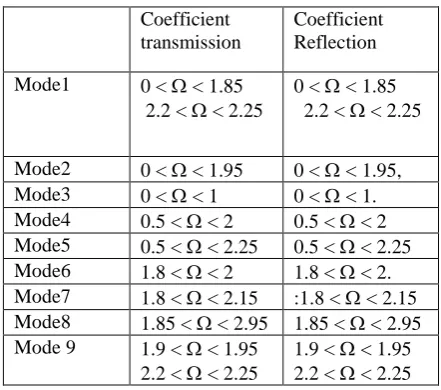
rij = (Vgi / Vgi) Rij² and tij = (Vgj / Vgi) Tij² (4) Where in order to obtain unitarity of the scattering matrix, the scattered waves have to be normalised with respect to their group velocity. Vgs is the group velocity of the eigenmode i, put equal to zero for evanescent modes. Rij and Tij are respectively the reflection and transmission coefficients that describe the scattering of a given incident wave i into the eigenmodes i = 1, 2, 3, 4, 5, 6, 7, 8, 9. The transmission and reflection coefficients related to vibrational mode 1 and 9 are little modified with the variation of parameters of the system at the neighbourhood of the defect. They spread respectively on band of frequencies summarised in table 1:
Coefficient transmission
Coefficient Reflection
Mode1 0 < < 1.85 2.2 < < 2.25
0 < < 1.85 2.2 < < 2.25
Mode2 0 < < 1.95 0 < < 1.95, Mode3 0 < < 1 0 < < 1. Mode4 0.5 < < 2 0.5 < < 2 Mode5 0.5 < < 2.25 0.5 < < 2.25 Mode6 1.8 < < 2 1.8 < < 2. Mode7 1.8 < < 2.15 :1.8 < < 2.15 Mode8 1.85 < < 2.95 1.85 < < 2.95 Mode 9 1.9 < < 1.95
2.2 < < 2.25
1.9 < < 1.95 2.2 < < 2.25
Table 1: Coefficient of transmission and reflection modes of the nanowell.
We can further define total reflection and transmission probabilities for a given eigenmode at scattering frequency by summing over all the contributions
ri() = jrij() and ti() = jtij()
(6)
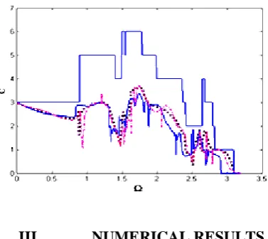
Fig. 1.
:
The curves of transmission t1, t2, t3, t4, t5 , t6, t7, t8 , t9 (doted-lines) and reflection r1, r2, r3, r4, r5, r6 , r7, r8, r9,coefficients (solid-lines) and their sum s1, s2, s3, s4 s5, s6, s7, s8 , s9 (solid lines) for homogeneous parameters:r1d=1, r2d = 0.8.
Furthermore, in order to describe the over all transmission of mesoscopic multichannel systems at a given frequency , it is useful to define the conductance of the system (or the domain defect transmittance) C(), by summing over all input and output channels[27-29].
C() = ij tij() (7)
Where the sum is carried out over all propagating modes at frequency . The transmission probabilities
ti() per eigenmode i, and the conductance of the system C() are important to calculate because each corresponds indeed to an experimentally measurable observable. thermal conductivity The wave guide conductance C() plays an essential role for vibrational and electrical propriety of the system.
III.
NUMERICAL RESULTS
We examined the coherent phononic transport in extended slab atomic well as function the incident energy and the parameters of neighbourhood of perturbed domain boundary . Also we consider particular possible homogeneous case, hardening and softening of the elastic force constants in the atomic slab nanowell region with respect to other regions far from the well . Consider in all cases that r = 0.8, which value characterizes realistic physical atomic structures in the bulk and surface regions. The transmission and reflection coefficients and the total conductance spectrum are calculated and presented respectively in Figure 1 for the homogeneous parameters r1d = 1, r = 0.8, r2d= 0.8, and Figure 2 for three different cases determining a
choice of the elastic properties of the atomic nanowell domain: softening: r1d = 0.9, r = 0.8, r2d=0.7.
and homogeneous: r1d = 1,r = 0.8, r2d= 0.8.
The total elastic-wave conductance of the system C(y, ), is a useful quantity to calculate, as it corresponds to an experimentally measurable observable, for example in heat transfer, it induced by sum of the propagating modes of the system; it undergoes the influence of the variation of the parameters of the system at the neighbourhood of the slab atomic nanowell. It spreads on a beach of frequencies corresponding to 0 < < 3.2, the phonon energy band; these curves of conductance varies according to parameters 1 and 2, and present peak resonances of different heights and widths, around frequencies = 0.95, 1.5 and 2.5, what gives it a rough aspect. One notes shifts of resonances peaks toward the high frequencies with the increasing parameters 1 and
2. The conductance spectra always starts with her higher values at low frequencies ( tend to zero), fluctuate for the intermediate values of and decrease with increasing then becomes zero at the Brillouin zone limit. Which the system reflects all the upper frequencies to 3.5 ( 3.5) and acts as a mirror for the elastic-wave, it plays the role of a frequential filter passes low. Another general characteristic of the total phonon conductance is the systematic displacement of its spectral maxima to higher frequencies with increasing hardening of the elastic constants in the nanowell domain. These maxima in the interval [0, 3.5] correspond to characteristic Fano resonancessince the vibration states on the nanowell domain are effectively localized at the nanowell domain, which interact with the continuum of the incident waveguide modes.
IV.
CONCLUSIONS
In this work, we have presented a calculation approach of the study of the coherent phononic transport spectra of the Slab atomic nanowell which acts as the joint between three sets of semi-infinite atomic multilayer. This analysis regarding the scattering properties of nanowell that transmission, reflection coefficient and total transmission of the system as function of the incident energy and the characteristic parameters of nanostructure domain .We note that the conductance of the system is related to measurable thermal conductivity of the nanostructure. This approach can be extend to other physical properties then the spin wave dynamic and electronic conductivity. We can also determined the heat capacity and
internal energy of the disordered system. The spectrum of different properties are the signature of the nature and crystalline configuration structural defects and can be used in the no destroyed control to investigate the reticular inhomogeneities in the studied system.
REFERENCES
[1] Lifshitz I. M. , and Kosevich A.M., Rep. Prog. Ph ys. ,1966, 29, p17.
[2] Vasseur J. O., Djafari-Rouhani B., Dobrzynski L, Akjouj A., and Zammouri, J., Phys. Rev. ,1999, B59, p.13446.
[3] Dobrzynski L., Djafari-Rouhani B., Akjouj A., Vasseur J. O., and Zammouri, J., Eur. Phys. Lett., 1999, 46, p.467.
[4] Akjouj A., Dobrzynski L., Djafari-Rouhani B., Vasseur J. O. and Kushwaha M. S. Eur. Phys. Lett., 1998, 41, p.321.
[5] Abou Ghantous M., and Khater A., Eur. Phys. J.B, 1999, 12, p.335. [6] Gagel F., and Maschke K., Phys. Rev. , 1995, B 52, p.2013.
[7] Szeftel J. and Khater A., J. Phys. C: Solid St. Phys.1987, 20, p.4725. [8] Pennec Y. and Khater A. , Surf. Sci. Lett.,1995,348, p. 82.
[9] Fellay A., Gage1 F., Maschke K., Virlouvet A. and Khater A., Phys. Rev.,1997,B55 ,p. 1707. [10] R. Landauer, J. Phys.: Condensed Matter 1, 1989, p. 899.
[11] A.R.P. Rau, Physica Scripta, 2004, 69,p. 1.
[12] R.Tigrine, A.Khater, O.Rafil, M.Belhadi and J.Hardy, Phys Stat Sol. (b), 2003, 239, p. 144 [13] H. Grimech and A. Khater, Surf. Sci. ,1995,323, p.198.
[14] M.Belhadi, A. Khater, J.Hardy and K.Maschke, Eur.Phys.J.Appl.Phys., 2006, 35, p.185. [15] M. Buttiker, Y. Imry, R. Landauer, S. Pinhas, Phys. Rev. , 1985,B31, p.6207 .
[16] A. Maradudin, R. F. Wallis and L. Dobrzynski, Handbook of Surfaces and Interfaces, Volume 3 Garland, New York (1980)
[17] Alessandra F., Vilela.,A , Gargano.R.,Geraldo M., e S, Impurity effects on solitons in conjugated polymer linking model hamiltonians and ab initio method descriptions, Journal of molecular structure,2006, 769, pp.33-37.
[18] Celso .P., de Melo, Humberto S., Brandi and Alfredo A. S., da Gama, Localized States in Polymeric Molecules III the Electronic Structure of Polyacetylene, Theoret.Chim.Acta (Berl),1983,pp. 63, 1-8. [19] Tanner. D.B., Doll, G.L., Raob, A.M., Eklund, P.C., Arbuckle, b, G.A., MacDiarmid, A.G., Optical
[20] Ziegler.K, Symmetries and broken, Symmetries in a model of disordered, polyacetylene, Z.Pys.B, Condensed, Matter, 1990,78,pp. 281-288.
[21] Rafil.O., Tamine.M. Bourahla.B. Tigrine.R. and Amoudache.S. and Kather.A, Modifying polyacetylene, Chinese Journal of polymer Science , 2006,24, pp.229- 236.
[22] Landauer,R.,Electrical resistance of disordered one-dimensional lattices, Philos. Mag.1970, pp.863-867..
[23] Büttiker, M. , Four terminal phase coherent conductance, Phys. Rev. Lett,1986, 57,pp. 1761-1764. [24] Belhadi, M. , Khater, A., Hardy, J., Maschke, K. , Phonon transmission via a three-terminal junction in
low dimensional wave-guide, Eur. Phys. J. Appl. Phys.,2006, 35, p.185.
[25] Belhadi, M., Chadli, R., Khater, A. and Abou Ghantous, M., Spin dynamics across an in homogeneous atomic boundary separating ultrathin Heisenberg ferromagnetic films.Eur. Phys. J. Appl. Phys., 2007,37, p.25.
[26] Szeftel.J and Khater.A., Calculation of surface phonon and resonances: the matching Procedure: I, J.Pysic.C, solid stat phys, 1997,4725, pp. 4736, 1987.
[27] Szeftel, J., and Khater, A., Calculation of surface phonons and resonances: the matching procedure: I, J. Phys. C, Solid State Phys,1987,pp. 4725-4736.
[28] Felley, A., Gagel, F., Maschke, K., Virlouvet, A., Khater, A., Scattering of vibrational waves in perturbed quasi-1D multichannel wave guides, Phys. Rev., 1997, B, 55,pp. 1707-1717.