Karimov et al. World Journal of Engineering Research and Technology
PHYSICAL-TECHNOLOGICAL ASPECTS OF A
MULTIFUNCTIONAL SENSOR BASED ON A FIELD-EFFECT
TRANSISTOR
Karimov A.V.*1, Djurayev D.R.2, Turaev A.A.2
1
Physical-Technical Institute, Uzbekistan Academy of Sciences, Tashkent, Uzbekistan.
2
Bukhara State University, Bukhara, Uzbekistan.
Article Received on 05/01/2017 Article Revised on 01/02/2017 Article Accepted on 20/02/2017
ABSTRACT
The physical and technological criteria are presented for providing to
the junction field-effect transistor sensitivity to external influences. It
is shown that in the channel depletion mode by drain-gate voltage
photosensitivity of drain-gate junction or temperature sensitivity of
pinch-off voltage are greater than in the other modes.
KEYWORDS: field-effect transistor, pinch-off voltage, photosensitivity, channel thickness.
INTRODUCTION
Now the non-trivial modes of field and bipolar transistor operation are of great interest. It was
found that a two-source transistor is very sensitive to deformation (Babichev et al, 2000). A
field-effect transistor produced as a two-transistor cell with series-connected channels greatly
amplifies direct and alternate signals (Karimov et al, 2015a). For a field-effect transistor to be
sensitive to external actions, such transistor is proposed to operate in a mode of channel
blocking by source-gate voltage and pinch-off voltage to be used as a measuring parameter
(Karimov et al, 2015b).
This paper presents the field-effect transistor operation as a multifunctional sensor in a mode
of channel blocking by source-gate voltage. *Corresponding Author
Karimov A.V.
Physical-Technical
Institute, Uzbekistan
Academy of Sciences,
Tashkent, Uzbekistan.
World Journal of Engineering Research and Technology
WJERT
Field-effect transistor
A multifunctional sensor was produced on the basis of silicon. An epitaxial layer of the n
-type conduction with the carrier concentration 2·1015 cm-3 and the thickness 0.7-1.5 μm (its
optimal values are presented in Table 2) was grown on a silicon р+-substrate of 200 μm in
thickness and with the carrier concentration 1·1019cm-3. Then the contact regions were
formed by deposition of indium and silver through windows in a mask. The distance between
source and drain, i.e. the channel length, was equal to 150-200 μm. On the back side of the
substrate a continuous contact was formed by indium and silver deposition.
One of the design-technological features of the field-effect transistor under study is that the
channel is accessible for external action (Fig.1). For the rapid reaction to changing
temperature it is necessary that the substrate thickness should be as thin as possible, i.e. not
200 μm as we have but about 100 μm.
Fig.1: A structure of investigated field-effect transistor.
Main criteria for selection of parameters of field-effect transistor as a multifunctional sensor.
As shown in Fig.1, the junction field-effect transistor consists of a low-resistance substrate of
the first type with the lower electrode of gate, an epitaxial (diffusive) high-resistance layer of
the second type with the ohmic contact regions of source and drain; between them there is a
channel of L in length and
а
in thickness that is 2 more than the initial thickness of thedepletion layer of the p+-n-junction. This thickness provides a value of the channel pinch-off
voltage twice as large as the diffusion potential UD, Ucutoff 2UD. The thickness of the
depletion layer of the p+-n-junction decreases with temperature increase or under light
For optimal modulation of channel under external action, the pinch-off voltage is taken
according the equality Ucutoff 2UD. As given in Table 1, for the zero shift the bulk charge
thickness is 0.65 μm and the contact difference of potentials is 0.61 V. Then for the pinch-off
voltage of 0.61 V we have х2 =1.22 V or for the reverse channel-gate voltage Ureverse=0.6 V
we have the thickness Wbchr=0.90 μm, i.e. when the voltage increases twice as much the bulk
charge region (bchr) increases as much as 2 , which corresponds to the optimal thickness of
the channel.
Table 1: Thickness of bulk charge layer vs. reverse voltage.
Ureverse, V 0.0 0.1 0.2 0.4 0.6 0.8 1,0 1.3 1.6
bchr
W , μm 0.65 0.70 0.74 0.83 0.90 0.97 1.04 1.13 1.22
Selection of the channel thickness within 2 of the bulk charge region thickness of the p-n
-junction is due to the fact that for large thicknesses the field-effect transistor sensitivity to
external actions decreases and for smaller ones there is a possibility of hysteresis formation
when the pinch-off voltage increases and decreases under external actions because of
enlarging or narrowing the bulk charge region caused by a sharp reduction in the carrier
concentration near the p-n-junction boundary.
The special point of our multifunctional sensor is that if for the available thermosensitive
field-effect transistor the negative temperature coefficient of the channel conduction
dependence is suppressed owing to selecting the carrier concentration near the transition
point of temperature sensitivity of mobility from high values to low ones (Karimov and
Bakhronov, 1999) then in our case there should be photo-sensitivity and pressure-sensitivity
besides temperature one. Those features can be provided if the field-effect transistor operates
in a mode of channel blocking by the drain-gate voltage when with the raise in the working
voltage before channel pinch-off the voltage drop on the source-gate junction linearly
increases and then after pinch-off becomes equal to channel pinch-off voltage. For a specified
working voltage the action of light or temperature (pressure) on the channel leads to changes
in potential at the source-gate junction that is identified as a measuring parameter, as
Experimental results and discussion
Under illumination of the channel in the bulk charge region of the gate-channel junction the
electron-hole pairs are generated; they create a photo-current at the source-gate junction
leading to a decrease in resistance of this junction, which results in turn in the voltage drop
and in a corresponding increase of the drain current. An electronic scheme of how to measure
the dependence of the voltage drop at the source-gate junction on external action is presented
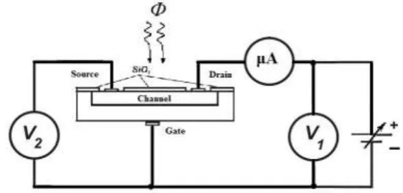
in Fig. 2.
Fig. 2: A scheme of measuring the voltage drop at the source-gate junction in a mode of channel blocking by the drain-gate voltage.
As seen from the figure, the gate-channel junction operates in a diode mode or under
illumination it operates similar to a photodiode. However, in principle it essentially differs
from a photodiode. In the offered working mode of channel blocking the voltage at the
drain-gate junction is two times and over more than that at the source-drain-gate junction. When the
source output is closed with the drain one (diode mode) it is transformed into a diode with a
thin base.
As given in Fig.3, in the diode mode the reverse current up to 10 V does not exceed 1 nA and
in the forward direction beginning with 0.7 V a sharp increase in current is observed and for
the voltage 0.9 V the direct current is 9.75 mA. Accordingly, in the mode of channel blocking
the so insignificant reverse current of the gate-source junction will not make effect on
-10 -8 -6 -4 -2 00 3 6 9 12 15
Urev, В
Irev, mкA Idir, mA
Udir, В
Fig. 3: The voltage-current characteristic of the drain-gate junction.
As shown by the investigation, in the short circuit mode when the gate and source outputs are
connected with an ammeter the photocurrent increases almost linearly (Fig. 5, Curve 1) with
the raise in the intensity of channel illumination by a halogen lamp. In the mode of channel
blocking by the drain-gate voltage we have the photocurrent as large as twice (Curve 2).
0 1000 2000 3000 4000
0 1 2 3 4
Ph, lux
Iph, mkA
2
1
Fig. 4: The dependences of photocurrent on illumination intensity in the short-circuit mode and for channel blocking by the drain-gate voltage.
As far as the voltage drop is concerned, its value with the raise in illumination intensity
significantly decreases for the small intensities of illumination and further non-linearly
decreases and the dependence becomes weak. For the first region the sensitivity is 0.00025
V/lux and for the region 1000-2000 lux the photo-sensitivity is an order less and equal to
0 1000 2000 3000 4000 0,80
0,82 0,84 0,86 0,88 0,90 0,92
Ugs, V
Ph, lux
Fig. 5: The dependence of voltage drop at the gate-source junction on illumination in the mode of channel blocking by the drain-gate voltage.
The fact that the voltage drop at the source-gate junction is sensitive to illumination can be
explained as follows. Channel illumination by n-type quanta with the energy greater than the
bandgap leads to generation of non-equilibrium electron-hole pairs and an increase in
illumination intensity to a decrease in the contact difference of potentials of the p-n-junction
ph n ph
n n
n e
kT U
ln ,
where nрh - is the concentration of holes generated by photons under illumination of the
n-region.
In turn, the photocurrent appearing at the source-gate junction reduces its resistance, which
leads to a decrease in the dropping voltage as compared with the dark one.
consumption (Karimov et al., 2013). When the temperature increases from room one to
100oC the pinch-off voltage increases from 0.92 V to 1.0 V. The temperature coefficient is 2
mV/degree, which is within the range obtained for the diode structures in the mode of direct
current restriction up to 10 mA (Kurashkin, 2011).
CONCLUSION
Thus, it is experimentally shown that in the mode of channel blocking by the drain-gate
voltage and the use as a measuring parameter of the pinch-off voltage the field-effect
transistor with bottom gate and open channel has temperature and illumination sensitivity
greater than that of other modes of operation. The power voltage is 2-5 V for the current less
than 10 µA that is three orders less as compared with the diode mode.
REFERENCE
1. Babichev G G, Kozlovskiy S I, Romanov V A and Sharan N N. “Silicon two-source
field-effect tensotransistors”, Journal of Technical Physics, 2000; 70(10): 45-49.
2. Karimov A V and Bakhronov Sh N. “The thermoelectric converter”, Technical Physics
Letters, 1999; 25: 101–102.
3. Karimov A V, Yodgorova D M, Abdulhaev O A, Kamanov B M and Turaev A A.
“Features of the temperature properties of a field-effect transistor in a current-limiting mode”, Journal of Engineering Physics and Thermophysics, 2013; 86(1): 248-254.
4. Karimov A V, Yodgorova D M, Kamanov B M, Djurayev D R and Turayev A A.
(2015a), “Features amplifying properties of a field effect transistor in the circuit with dynamic load”, Physical Surface Engineering, 2015: 13(1): 12-16.
5. Karimov A V, Yodgorova D M, Abdulkhaev O A, Dzhurayev D R and Turaev A A
(2015b) “Multi-sensor-based field-effect transistor”, Patent RUz IAP05120.
6. Kurashkin S F. “The use of semiconductor diode as a measuring input the