warwick.ac.uk/lib-publications Manuscript version: Author’s Accepted Manuscript
The version presented in WRAP is the author’s accepted manuscript and may differ from the published version or Version of Record.
Persistent WRAP URL:
http://wrap.warwick.ac.uk/115518 How to cite:
Please refer to published version for the most recent bibliographic citation information. If a published version is known of, the repository item page linked to above, will contain details on accessing it.
Copyright and reuse:
The Warwick Research Archive Portal (WRAP) makes this work by researchers of the University of Warwick available open access under the following conditions.
Copyright © and all moral rights to the version of the paper presented here belong to the individual author(s) and/or other copyright owners. To the extent reasonable and
practicable the material made available in WRAP has been checked for eligibility before being made available.
Copies of full items can be used for personal research or study, educational, or not-for-profit purposes without prior permission or charge. Provided that the authors, title and full
bibliographic details are credited, a hyperlink and/or URL is given for the original metadata page and the content is not changed in any way.
Publisher’s statement:
Please refer to the repository item page, publisher’s statement section, for further information.
1
Nanoscale Electrochemical Mapping
Cameron L. Bentley,1 James Edmondson,1,2 Gabriel N. Meloni,1 David Perry,1 Viacheslav Shkirskiy,1 Patrick R. Unwin1,*
1Department of Chemistry, 2MAS Centre for Doctoral Training, University of Warwick, Coventry, CV4 7AL, United Kingdom
2
1. Introduction
Surfaces and interfaces, of both practical and fundamental interest, have long been recognized
to be complex, yet while there are many microscopy and spectroscopy methods for imaging
structure, topography and surface chemical composition at high spatial resolution, there are
relatively few techniques for mapping associated chemical fluxes in the near-interface region.
In this regard, scanning electrochemical probe microscopy (SEPM), which utilizes a small
scale electrode probe as an imaging device, has had a unique place in the scanning probe
microscopy (SPM) family of techniques, in being able to map chemical fluxes and interfacial
reactivity. For a long time, techniques such as scanning electrochemical microscopy (SECM)
were largely stuck at the micron – or larger – scale in terms of spatial resolution, but recent
years have seen spectacular progress, such that a variety of different types of SEPM technique
are now available and 10s of nm spatial resolution is becoming increasingly accessible. This
step-change in capability is opening many new opportunities for the characterization of flux
processes and interfacial activity in a whole raft of systems, including electrode surfaces,
electromaterials, soft matter, living cells and tissues.
Most of the significant developments in nanoscale SEPM have occurred since 2010 and
a previous review in this series captured major advances in scanning ion conductance
microscopy (SICM), SECM, scanning electrochemical cell microscopy (SECCM) and hybrids
of these techniques primarily in the period 2014-16.1 We also produced a review article in 2016
that described new frontiers that are being opened up from advances in nanoscale
electrochemical imaging.2 Mainly covering the past 3 years, the present article highlights
advances in each of the main SEPM techniques, and various hybrid SEPM methods. We also
cover electrochemical - scanning tunneling microscopy (EC-STM), where there have been
interesting developments in high-resolution electrochemical mapping and in determining
changes in electrode structure in electrochemical processes, which has been the main traditional
use of EC-STM. We note in passing that there has been considerable progress in single
molecule conductance and electrochemistry studies with EC-STM, as highlighted in recent
reviews,3,4 but this field is beyond the scope of this article.
In selecting material for inclusion in this article, we have used the common definition
of nanoscale as being 100 nm or smaller, and conveniently use the tip radius as the measure.
We note that there is a wealth of literature concerning SECM that uses micron or larger scale
3 of SECM with sub-micron scale resolution that will be of interest to the nanoscale community
and so we reference these as appropriate. SICM and SECCM easily attain the nanoscale
definition, due to the ease of fabrication and use of nanopipet probes, and the fact that these
techniques incorporate and measure substrate topography, as well as other functional
properties. We have recently reviewed aspects of both techniques over the past 2 years.5,6 Some
other SEPM-related methods have remained at the 10s of micron scale and we briefly mention
these later as areas where there is room for innovation.
Alongside developments in SEPMs, various optical methods are increasingly finding
application for visualizing electrode activity, and during the period covered by the review there
are initial signs of the combination of SEPMs and optical techniques. We thus very briefly
mention some of these methods, noting that there have been recent reviews that include
electrochemical applications of super-resolution microscopy, plasmonic-based imaging
techniques and holography.7,8
With the translation of SEPM to the nanoscale, the preparation and understanding of
the behavior of nanoelectrodes and nanopipets is imperative, for which there are recent
scholarly reviews.9,10 We also point the interested reader to relevant reviews from the period
that cover SECM characterization of electrocatalysts, 11 a very recent review on the application
of SEPM in general to electrocatalysis,12 microelectrochemical studies of corrosion,13 and
high-resolution investigations of energy storage materials.14,15 The most comprehensive review
of SECM ever written, which serves as a practical guide to the new entrant and experienced
researcher alike, was also published in the period.16 The popularity of SECM, in particular, and
SEPM in general, for single cell electrochemical imaging and life sciences applications, is
reflected in a number of recent review articles.17-22
SEPM is a key enabling technology for the emerging fields of single entity
electrochemistry and electrochemistry at nano-interfaces, for which there were seminal
Faraday Discussion meetings in 2016 and 2018, respectively. The published volumes of these
meetings23,24 contain not only original papers, but also extensive discussions of key issues. A
very recent perspective of single entity electrochemistry places SEPM techniques alongside
4
2. Scanning Electrochemical Microscopy (SECM) 2.1 Overview of Operational Principles
SECM is the best-known technique in the SEPM family and has been widely adopted since its
inception in the late 1980s.26,27 The operational principles of SECM and its applications have
been covered in a number of recent reviews.16,28-30 Using small-scale electrodes (originally
micron-scale ultramicroelectrodes, UMEs, and most recently nanoelectrodes, Section 2.2) as a
scanning probe tip, SECM is capable of resolving either the topography or (electro)chemical
activity (albeit not usually simultaneously) of substrates immersed in a solution (electrolyte)
bath. This is achieved by monitoring the electrochemical response of the scanning tip when it
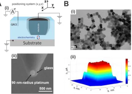
is brought into close proximity with a substrate surface (e.g., Figure 1A-i). In essence, the
extent and nature of the perturbations caused by the substrate on the recorded signal at the
SECM tip is used to infer on the substrate properties.31,32 For instance, considering the most
simple amperometric tip, an insulating substrate hinders the diffusion of an electroactive solute
towards the tip, resulting in a diminished current (i.e., negative feedback),26,31 while a
conducting substrate poised at the appropriate potential (externally biased or unbiased) may
regenerate the active species, enhancing the tip current by creating a positive feedback loop, or
redox shuttling between the tip and surface (as in Figure 1A-i).
While involving UMEs on the hundreds of nm to micron-scale and not mapping, it is
worth mentioning that recent work has sought to decrease the gap size in dual-electrode SECM,
where a tip electrode is positioned close to a substrate electrode, to create a device with high
tip-substrate diffusion rates of soluble redox couples, thereby extending the upper kinetic limit
accessible for the measurement of fast electron-transfer kinetics33 and the detection of
short-lifetime transient species.34,35 A small gap size, however, requires careful analysis and
modeling of ion migration36,37 and double layer effects at the electrodes33,36,38 and the glass or
quartz sheath38 that surrounds the active part of the tip. Thus, recent treatments of
mass-transport in SECM have considered solutions to the Nernst-Planck equation and Poisson
equation with charged interfaces.38 Such considerations extend to nanoscale SECM probes
used for imaging, which are usually deployed close to the substrate (within a distance of a tip
radius or so).
As the first SEPM, SECM continues to be widely used,39,40 and is applicable to a range
of chemical and electrochemical systems.1,16,17,28,29,41,42 There have been recent interesting
5 acquisition rates.43 However, as conventional SECM lacks independent positional feedback of
the tip and relies on constant height scanning,16,44 there are naturally practical limitations when
attempting to investigate (electro)chemical systems at the single entity level, e.g., single
nanoparticles (NPs) or particular sites on a complex surface such as step edges, defined
crystallographic facets or grain boundaries (GBs), for which nanoscale electrochemical flux
mapping is proving to be particularly powerful.45,46 Significant efforts have being made in the
past half-decade to use multifunctional probes and combined techniques,2,47 as described later
in this article. Here, we consider recent efforts towards nanoscale reaction mapping by
translating conventional SECM methods and instrumentation.
2.2 Approaching the Nanoscale with SECM
A recent review has discussed the translation of SECM to the nanoscale.40,44 Considerations
for nanoscale SECM probe tips include ease of fabrication, lifetime, reproducibility and
electrochemical behavior over the long periods of a scan, and technical issues around
positioning and scanning within a distance of a tip radius or so from a surface (i.e., 10s of nm),
in a constant height mode, without independent distance control or positional feedback. To
address this issue, a few innovative approaches are worth mentioning, such as the use of a
hopping scan protocol, where the scanning (nanoelectrode) tip performs an approach curve
from bulk solution towards the substrate at every image pixel of an electrochemical map. By
comparing the current recorded at bulk with the one near the surface, the electrode can be
stopped consistently at a desired current variation (i.e., feedback set-point, albeit that the
substrate activity must be known a-priori). This approach effectively eliminates instrumental
drift, such as thermal drift of the piezoelectric actuators commonly used for tip positioning,48
allowing the tip to be precisely positioned near the substrate and, due to the retract distance
adopted during the hopping procedure, used to scan substrates with pronounced topographical
features.49
Another recent approach to solve the problem of precisely approaching a tip close to a
substrate surface involves partially modifying the interface (e.g., with a flexible polymer spot)
to make it “soft”.50 This “soft” interface allows the tip to be approached very close to (and even
into contact with) the surface, without sustaining significant damage (i.e., change in tip
geometry and/or electrochemical response). The “soft” nature of the substrate also allowed for
fast tip approaches to be performed, at speeds up to 100-fold the ones normally employed in
6 approached to the “soft spot” at the substrate, the tip can be laterally translated to a “hard” area
of the substrate, allowing this approach to be employed with a range of different materials.50
Interestingly, this latter approach to positioning electrodes also has significant
implications for the characterization of nanoelectrodes. At the nanoscale, SECM probes are
often, but not exclusively,51 solid electrodes that consist of a conductive material (commonly
noble metals or carbon) encapsulated within an inert insulating material (e.g., glass or quartz)
outer sheath.52,53 While the dimensions of conventional (micron to 10s of micron scale
electrode) SECM probes are readily determined (e.g., the size of the metal wire used is known,
visual inspection is easily made by optical microscopy, and steady-state voltammetry reveals
the electrode size and dimensions54), such easy methods obviously do not translate to the
nanoscale. In particular, voltammetric measurements alone may provide misleading
information regarding the true electrode size and geometry,55,56 because an idealized geometry
has to be assumed and small imperfections can have a significant effect on nanoscale
mass-transport and the associated voltammetry. Approach curves towards soft substrates, mentioned
above, also provide critical information regarding the tip geometry without the risk of
destroying the tip.50 Nonetheless, non-ideal tip geometry and tip-substrate misalignment can
still significantly impact the electrochemical response in SECM approach curves, and thus the
careful use of electron microscopy (notably transmission electron microscopy, TEM) to allow
the proper characterization of small-scale SECM probes is increasingly advocated.57 Accurate
knowledge of tip geometry is essential for quantitative analysis of experimental data with
simulation models.38,58-61
2.3 Fabrication of Nanometer-sized SECM tips
There are a number of reports on the fabrication of metal electrodes on the sub-100 nm scale.
42,62,63 Due to the large impact of electrode geometry on the electrochemical response, further
fabrication steps are often used to shape the electrode and thus tailor its electrochemical
response.64-66 On this note, focused ion beam (FIB) milling can be an important step, used to
sculpt a tip to the desired geometry,66,67 as in the tip shown in Figure 1A-ii,65 although this
obviously extends the complexity and cost of tip manufacture. Such tips have been used to
image nanomaterials, as summarized in Figure 1B, which we discuss in more detail below.
Recent efforts have demonstrated that the fabrication of nm-sized electrodes, with geometries
suitable for SECM experiments, can be achieved using less expensive and time-consuming
7 with resistive coil-based heating and thus using glass capillary tubes (instead of quartz), Pt
nanoelectrodes were fabricated and successfully employed for high-resolution imaging of
metallic substrates (Pt and Ti nano-bands and single AuNPs anchored to a thiol-covered Au
substrate) and the catalytic activity of lactate-oxidase modified Au substrates.49,68 It should also
be noted that some laboratories have reported that nm-sized metal electrodes can be easily
damaged without severe precautions,44,69 which adds to the costs and time demands involved
in the fabrication and handling of SECM tips.
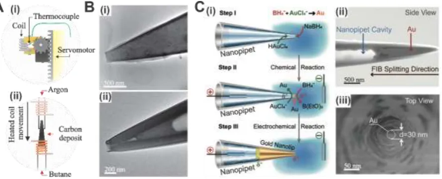
An ingenious alternative for making SECM tips is based on the pyrolysis of a carbon
source (usually butane gas) under an Ar atmosphere to produce carbon inside freshly pulled
quartz nanopipets,55,70 as originally introduced by Takahashi et al.68 and developed by others.53
This is a relatively fast method, but as it is a manual procedure, the creation of a tip electrode
that is flush with the end of the surrounding quartz sheath is something of an art, with recessed
(inside of the pipet bore), overfilled or damaged electrodes being commonplace. An advantage
of these probes is that the carbon filling is readily visualized with TEM and FIB can be used to
square off a recessed electrode,42,71 as with metal nanoelectrodes, discussed above. A more
sophisticated approach to the carbon pyrolysis fabrication method was recently reported, based
on the use of an automated robotic system (Figure 2A-i and ii), resulting in a higher success
rate, reproducibility and quality of nm-sized carbon tips.57 By removing the inherent
inaccuracies of the manual operation procedures used previously, the influences of multiple
pyrolysis parameters on the final SECM tip geometry were elucidated, leading to a more robust
and reproducible fabrication protocol (Figure 2B).
Recent reports have explored the use of different solution compositions inside the
nanopipet and in the bulk solution in which the tip is placed to drive the formation of metallic
NPs in the pipet bore where the two solutions contact. The resulting structures can behave as
bipolar electrodes, and metal electrodeposition can be precisely controlled and monitored by
applying a driving potential between a quasi-reference counter electrode (QRCE) located inside
the pipet and one in bulk solution, yielding nanometer-sized metal electrodes (Figure 2C). This
approach can reportedly produce electrodes quickly and reproducibly, with radii on the 10s of
nm scale, and robust electrochemical responses,72-75 ideally suited to mapping electrochemical
substrate properties with nanoscale resolution.74 Pt has also been grown at the end of a
nanopipet and at nanopores using FIB to make bipolar nanoscale electrodes and such an
8 SECM with tips on the sub-micron to 100s of nm scale have been deployed for
electrochemical mapping of a wide spectrum of processes, ranging from studies of the
corrosion of steel,78 electrochemical characterization of complex electrocatalytic materials,79
assessment of basal surface and step-edge redox activity in MoS2 devices,80 ion intercalation
into graphene,81 and investigation of charge storage capacity on redox active colloids.82 The
latter study is particularly noteworthy as it involved the use of SECM on a Raman microscopy
platform. The combination of SECM and other SEPMs with co-located microscopy or
micro-spectroscopy is a developing trend that is proving powerful for providing holistic views of
structure-function at high spatial resolution. Beyond the investigation of electrodes and
electroactive materials, SECM with nanoscale probes continues to be popular in life sciences
applications, for example, investigating molecular uptake at the single cell level.61
Recent works have also showcased SECM measurements on the 10s of nm scale, such
as the investigation of the homogeneity and passivity of thiophenol diazonium films
graphitized over highly ordered pyrolytic graphite (HOPG) substrates.83 The properties of the
surface heterogeneities (e.g., pinhole defects) towards electron-transfer reactions were
elucidated with high spatial resolution. By employing 10-20 nm radius Pt SECM tips, it was
shown that single spherical NPs (as small as 10 nm in radius) could be resolved,84 as well as
the electrochemical properties of single Pd nanocubes (14 nm sides), as in Figure 1B.83
Intriguingly, in the latter study, although there was a degree of correlation between the
geometry of the nanocubes obtained by SECM and TEM images (compare Figure 1B-i and ii),
the sharpness of the electrochemical image, especially at the cube edges, obtained with a
constant height scan, cannot be accounted for by considering only the diffusional current at the
tip. Other effects were suggested to influence the recorded signal, notably electron tunneling
between the tip and surface, although the constancy of the current across the top of a particle
would correspond to a remarkably consistent tunneling gap size (Section 5.4).
It is evident from some of these examples that scanning a nanoscale SECM tip within a
radius or so distance from a surface with no feedback could be restrictive in terms of the
samples that can be imaged. Evidently, without positional feedback, the degree of
topographical variation would need to be rather small compared to the tip size, to avoid tip
crash, while also noting that the sensitivity and spatial resolution of SECM to surface processes
is strongly dependent on the local tip-substrate separation.32,85 A general lack of independent
tip positioning capability in SECM leads to the well-known convolution of
9 mediators (i.e., one to indicate on topography and the other to measure reactivity)86 and a very
interesting recent approach is to use super-resolution optical imaging to track the tip position,
although this requires an optically transparent substrate.87 An important trend has been the
combination of SECM with other SPM methods, such as SICM, scanning tunneling
microscopy (STM) or atomic force microscopy (AFM).44 These hybrid techniques are
summarized, and recent developments reviewed in Section 5.
Figure 1. (A)(i) Schematic of a simple SECM setup, highlighting redox shuttling between a substrate and tip electrode. Provided the tip and sample currents are small, a QRCE can be
used, rather than individual reference and counter electrodes. (ii) SEM image of a FIB-milled, Pt nanoelectrode, used as a SECM tip for single NP electrochemical imaging ( reproduced from
Kim, J.; Renault, C.; Nioradze, N.; Arroyo-Currás, N.; Leonard, K. C.; Bard, A. J. J. Am. Chem.
Soc. 2016, 138, 8560-8568 (Ref 63). Copyright 2016 American Chemical Society). (B) (i)
TEM images of 14 nm sided Pd cubic NPs and (ii) positive-feedback electrochemical image of one of the cubes obtained with a 10 nm radius Pt nanoelectrode (SECM tip) in a 1 mM
ferrocenemethanol (FcMeOH) solution. Reproduced from Blanchard, P. Y.; Sun, T.; Yu, Y.;
Wei, Z.; Matsui, H.; Mirkin, M. V. Langmuir 2016, 32, 2500-2508 (Ref 83). Copyright 2016
[image:10.595.89.521.204.511.2]10
Figure 2. (A) Schematic of an automated heating system employed for the fabrication of carbon nanoelectrodes based on the pyrolysis of butane under an inert (Ar) atmosphere. (i)
Automation components, such as heating coil, servo motor and thermocouple (for precise
temperature control). (ii) Coil movement along the nanopipet length resulting in carbon pyrolysis inside the nanopipet bore. Highlighted are Ar and butane inlets and the coil movement
direction. (B) TEM images of carbon nanoelectrodes fabricated using the automated pyrolysis method. Due to the fine control of the temperature and pyrolysis time, tips can be produced
with (i) a completely filled carbon layer flush to pipet bore or (ii) a hollow carbon layer that can be used as a nano-sampler. (B) was reproduced from Towards Reproducible Fabrication of
Nanometre-Sized Carbon Electrodes: Optimisation of Automated Nanoelectrode Fabrication
by Means of Transmission Electron Microscopy, Wilde, P.; Quast, T.; Aiyappa, H. B.; Chen,
Y.-T.; Botz, A.; Tarnev, T.; Marquitan, M.; Feldhege, S.; Lindner, A.; Andronescu, C.;
Schuhmann, W. ChemElectroChem, Vol. 5, Issue 11 (Ref 57). Copyright 2018 Wiley. (C)
Metallic nanoelectrodes fabricated by the bipolar deposition method. (i) Schematic representation of the fabrication procedure from the nucleation of the first NP at the pipet bore
to the electrochemical deposition and growth of the metallic layer inside the pipet. (ii) SEM of a nanoelectrode produced from the bipolar growth method, FIB cut along its length to reveal
the depth of the metallic layer growth. (iii) SEM top view of a fabricated nanoelectrode. Reproduced from A 30 nm Nanopore Electrode: Facile Fabrication and Direct Insights into the
Intrinsic Feature of Single Nanoparticle Collisions, Gao, R.; Ying, Y. L.; Li, Y. J.; Hu, Y. X.;
Yu, R. J.; Lin, Y.; Long, Y. T., Angew. Chem., Int. Ed., Vol. 57, Issue 4 (Ref 72). Copyright
[image:11.595.79.524.71.251.2]11
3. Scanning Ion Conductance Microscopy (SICM) 3.1 Operational Principles
Traditionally, SICM has been used as a tool for mapping surface topography, most notably for
elucidating and tracking morphological changes in soft, living systems, such as biological
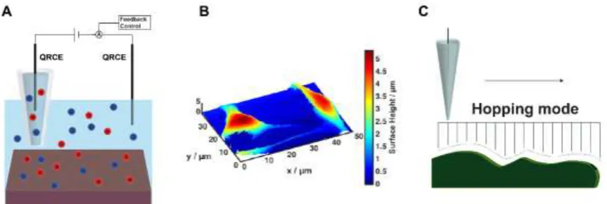
cells.88-90 A schematic of the SICM configuration, together with an example topographical map
of PC12 cells on a glass slide, is shown in Figure 3A and B. SICM measurements involve
bringing a nanopipet filled with an electrolyte solution to the vicinity of a surface of interest.
To ensure that there is no contact between the nanopipet and the surface, a bias is applied
between a QRCE inserted inside the nanopipet and a second QRCE in bulk solution to generate
an ionic current, which is monitored continuously. When the probe is in bulk solution (more
than one tip diameter from the substrate), the ionic current is dominated by the nanopipet
geometry, nanopipet surface charge, and conductivity of the electrolyte solution.58 However,
when the position of the nanopipet is within one tip (internal) diameter of the surface, the gap
resistance between the end of the pipet and the surface influences the current. The conventional
view has been that the gap resistance increases, as the nanopipet-substrate distance decreases,
leading to a decrease in the ionic current magnitude, typically by around 1-2% percent at
practical tip-substrate separations, suitable as a set point for imaging.6,88 The ionic current can
thus be used as a feedback signal to maintain a constant tip-substrate separation as the
nanopipet tracks the topography of the substrate, either in a constant distance mode of
scanning,91,92 or more commonly in a hopping/standing approach mode,93,94 where the tip is
approached from bulk solution to the near-surface at each pixel, as depicted in Figure 3C. In
this mode, the bulk conductance current can be updated at each pixel, eliminating any issues
from drift of the SICM bulk current (should it occur). Topography data is constructed from the
z-position of the tip at the set point as a function of x-y position in the plane of the substrate.
Alternating current (AC) modes of feedback have also been implemented into SICM
measurements to improve stability,91,95,96 but at the expense of scanning speed. The biggest
advantage of SICM compared to alternative high-resolution topographical techniques like
contact or tapping mode AFM, is that there is no physical contact between the tip and surface,
12
Figure 3. (A) Schematic of a typical SICM setup together with a typical (B) SICM topographical map of PC12 cells under physiological conditions. (C) Schematic representation of hopping mode scanning with SICM. Reproduced from Page, A.; Perry, D.; Unwin, P. R.
Proc. R. Soc. A 2017, 473, 20160889 (Ref 6), with permission from the Royal Society of
London.
3.2 Functional SICM
Over the past few years, there has been a trend in SICM studies towards simultaneous
topography-functional imaging.6 That SICM can be used to probe surface properties other than
topography was evident in the first paper on SICM, where enhanced conductivity was recorded
when an SICM probe was over a pore in a porous sample.89 More recently, the ability to
sensitively detect variations in local conductivity has allowed SICM to map substrate surface
charge. This was first demonstrated for simple inert substrates in low ionic strength solutions
(~10 mM),98-100 where the Debye length is relatively large (~ 3 nm in aqueous solution).
As with SECM, it is important to address the extent to which the SICM current is
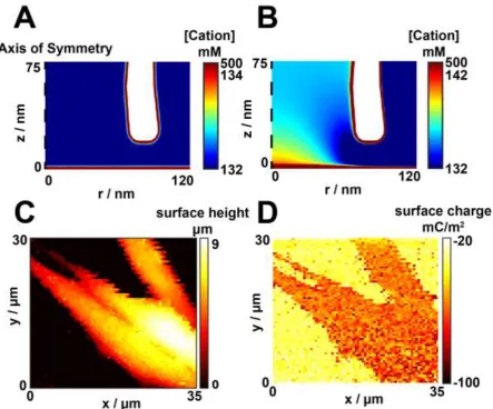
sensitive to topography compared to other properties, like surface charge. Finite element
method (FEM) simulations have proved particularly powerful for elucidating SICM protocols
that can be used to obtain topography and surface charge synchronously and independently.
98-102 In general, when there is a small SICM bias between the two QRCEs, the current is most
sensitive to topography, and essentially independent of surface charge.99 Under these
conditions the double layer at the surface is essentially unperturbed by the nanopipet (Figure
4A). At larger biases, however, the edge of the double layer is perturbed and sensed by the
significant electric field at the end of the nanopipet (Figure 4B). Further details about mapping
surface charge on the nanoscale and more recent developments are outlined below.
[image:13.595.75.507.71.216.2]13 There have been interesting recent morphological studies utilizing SICM,103-106 including the
combination of SICM data with co-located images from super-resolution microscopy (although
on separate instruments),107 which build on the established topographical capabilities of SICM.
There have also been a number methodological advances, including new scanning regimes and
instrumentation, which have resulted in a diversification in the uses of SICM. As highlighted
briefly above, modeling is an increasingly important part of SICM studies, allowing
experiments to be designed, and quantitative and meaningful information to be extracted from
experimental data. Some of the recent progress in each of these areas is outlined below.
3.3.1 Nanoscale Surface Charge Mapping with SICM. Interfacial charge has long been
recognized as being of key importance in determining the stability of colloidal systems and in
electrochemical processes. Areas where the role of surface charge is gaining increasing focus
include ionic crystal growth dynamics and various processes in living (cellular) systems, where
key functions such as cellular communication and uptake of nanomaterials are mediated by the
charge at the cell membrane.108,109 The protective properties of some corrosion products on
metals are also believed to be linked to the surface charge properties, mediating ion transport
during metal degradation,110 although the literature on this phenomenon is limited,111,112 mainly
due to the difficulty of measuring surface charge on metals directly in corrosive conditions.
SICM is emerging as a powerful methodology for surface charge mapping, with wide
applicability.6
Building on studies in relatively low ionic strength media (mentioned above),98-100 it
has subsequently been shown that surface charge mapping is possible under physiological
conditions, where the ionic strength is > 120 mM,101 as exemplified by synchronous topography
(Figure 4C) and surface charge (Figure 4D) mapping of mammalian cells. Several approaches
have been taken to elucidate surface charge and topography simultaneously using SICM. Initial
studies focused on using AC methods to elucidate topographical and surface charge
information.98,99 The first such approach used a distance-modulated feedback signal, whereby
a constant bias was applied between the two QRCEs during nanopipet scanning and the
nanopipet was oscillated vertically using a lock-in amplifier (amplitude ca. 20 nm, frequency
ca. 300 Hz). The resulting AC amplitude of the ion conductance current, measured with the
lock-in amplifier, was used to set a value for nanopipet positioning. The simultaneously
measured ionic current and AC phase signal were then analyzed to reveal surface charge
variations. A second approach used bias-modulation,95 whereby a small harmonic oscillation
14 that was detected with the lock-in amplifier and used as a set point to track surface topography.
Upon detection of the sample by the tip, the bias between the two electrodes was then swept
linearly over a range of a few hundred millivolts, such that the ionic current became sensitive
to surface charge. The advantage of this approach is that the contributions of topography
(nanopipet-surface distance) and surface charge to the ionic current response are easily
discerned. A similar approach has also been used to map the surface charge of
polydimethylsiloxane samples that have been patterned with either a positively or negatively
charged silane. In this approach, the rectification ratio at the positive and negative potentials of
the voltammetric sweep was used to infer the surface charge of the sample.102
Most recently, a new approach to charge mapping has been advocated, which greatly
speeds up the image acquisition times. This involves bringing the nanopipet near to the sample
surface with a bias applied, small enough to render the SICM ionic current to be relatively
insensitive to surface charge. Upon detection of the surface through a decrease in the ionic
current (increase in gap resistance), a short potential pulse (few 10s of milliseconds duration),
of a few hundred millivolts magnitude, is applied such that the ionic current becomes sensitive
to surface charge.113 This approach has been used to map both polymeric surfaces and living
cells.113 An alternative approach has utilized scanning charged samples at two distinct
nanopipet biases, one positive and one negative, and considering the difference in the obtained
height maps to inform on the effects of surface charge, as demonstrated for model charged
phospholipid bilayers.114 Whilst this approach could sacrifice some accuracy in the
topographical information obtained, and requires the near-surface ionic current to be less than
the bulk value (which may not always be the case),98,115 it does allow for faster imaging times
15
Figure 4. Simulated cation (K+) concentration under physiological conditions (~140 mM 1:1 electrolyte) near a charged interface (-80 mC/m2) with an applied tip bias of (A) -50 mV and
(B) 400 mV. These images are of the axisymmetric cylindrical geometry (that defines the tip-surface geometry and reduces the simulation problem to 2D).116 (C) Topographical and (D)
surface charge maps of PC12 cells under physiological conditions obtained synchronously in
a single scan using differential concentration SICM. Adapted from Perry, D.; Page, A.; Chen,
B.; Frenguelli, B. G.; Unwin, P. R. Anal. Chem. 2017, 89, 12458-12465 (Ref 116). Copyright
2017, American Chemical Society.
FEM simulations (typically carried out using the COMSOL Multiphysics software
package) are essential in order to extract quantitative information from the experimental data.
These simulations typically solve simultaneously the Poisson, Nernst-Planck and the
Navier-Stokes equations to determine the concentrations, electric field and electroosmotic flow,
16 response is knowing the nanopipet geometry accurately, and significant advances in probe
characterization (making use of TEM and current-voltage measurements) have come about in
recent years, allowing for more realistic simulations of SICM data.58,117
3.3.2 Nanoscale Electrochemical Flux Mapping. A new avenue for SICM is as a tool for
mapping electrochemical fluxes at electrode surfaces on the nanoscale. Electrochemical
processes are accompanied by changes in the ionic environment near the electrode surface, and
so the proven ability of SICM to probe local solution conductivity quantitatively offers
considerable prospects for visualizing electrode activity. A handful of studies, thus far,
demonstrate different approaches and the great promise of SICM as a powerful tool to elucidate
structure-activity relationships at electrochemical interfaces.
SICM reactivity mapping has been demonstrated in 2 different approaches, applied to:
(i) hydrazine oxidation and the hydrogen evolution reaction (HER); and (ii) the oxidation of
ferrocenemethyl trimethylammonium (FcTMA+) hexafluorophosphate, both at a platinum
UME.118 A hopping voltammetric approach was used to investigate the oxidation of hydrazine
and HER, whereby the SICM tip approached the substrate electrode surface at a potential where
there was no reaction (to map out the topography) and then the substrate potential was scanned
linearly to oxidize hydrazine and then reversed to cathodic potentials to drive HER, both
processes causing changed in local ionic conductivity that were sensed by the SICM tip. This
voltammetric process was repeated at a series of pixels to create a dataset that could be
reconstructed as a potentiodynamic movie of ion conductance maps as a function of substrate
electrode potential. For FcTMA+ electro-oxidation, a distance modulated approach was used
to sense the surface and obtain topographical information using an Archimedes spiral scan
profile to enhance the data acquisition rate. The topographical data were then used to set the
path of the tip during subsequent high-speed SICM reaction imaging, such that images of
16,000 pixels were obtained every 4 seconds, for a range of different potentials, with the tip
position automatically adjusted to maintain a constant tip-substrate separation in the course of
the scans. Data were presented as potentiodynamic movies of the nanopipet ionic current over
the area of interest as a function of driving potential (time). For both experimental strategies,
the movies highlighted clearly that there was a conductivity change around the UME as the
reactions progressed, as shown in the example images from the movie for FcTMA+ oxidation
17 A subsequent approach used a 30 nm diameter nanopipet and a DC ionic current
self-referencing hopping format, with a pulsed potential program applied to the substrate so as to
probe the surface topography and electrochemical reaction rate synchronously (Figure 5B
shows example data). At each pixel in the image, the SICM probe was brought into the vicinity
of the sample (to map the topography), with the electrode reaction “off” and a driving potential
was then applied to the substrate, which was either an Au UME or a carbon fiber UME with
electrodeposited catalytic AuNPs, to drive borohydride oxidation. Borohydride oxidation
results in significant depletion of the concentration of hydroxide ions, drastically reducing the
local conductivity of the solution, which was sensed by the SICM tip.119 By combining
experimental data, such as the representative examples in Figure 5B, with FEM simulations,
several interesting phenomena were observed. At low driving potentials for the oxidation, a
halo effect in conductivity around the NPs was apparent, due to depletion of ions in the gap
present between the NPs and the inert support. At higher driving potentials the region around
18
Figure 5. (A) Fast spiral scanning SICM reaction mapping of FCTMA+ oxidation at a 430 nm radius Pt UME sealed in quartz, with images at different applied potentials (vs. Ag/AgCl
QRCE) shown in (i-iv). Reproduced from Momotenko, D.; McKelvey, K.; Kang, M.; Meloni,
G. N.; Unwin, P. R. Anal. Chem. 2016, 88, 2838-2846 (Ref 118). Copyright 2016, American
Chemical Society. (B) Synchronous topographical and reaction mapping of borohydride oxidation at AuNPs on a carbon fiber support. Topographical maps (i,iii) and normalized ionic
current maps (ii,iv) obtained at low (i,ii) and high (iii,iv) driving potential. Experiments were
performed in 3 mM NaBH4 and 30 mM NaOH. Reproduced from Kang, M.; Perry, D.; Bentley,
C. L.; West, G.; Page, A.; Unwin, P. R. ACS Nano 2017, 11, 9525-9535 (Ref 119). Copyright
2017, American Chemical Society.
Dopamine oxidation at a carbon fiber electrode has also been visualized using SICM.116
In these studies, dopamine was present in the SICM tip but not in the bulk solution, and
[image:19.595.76.521.96.470.2]19 (hopping mode) using a fixed delivery potential applied to the SICM QRCE. Upon the
nanopipet detecting the surface, through a decrease in the ionic current, the substrate potential
was swept linearly from an initial value where there was no reaction to a value whereby
dopamine oxidation was driven at a diffusion-limited rate, with the resulting ionic current maps
and movies, as a function of potential, revealing the activity around the carbon fiber electrode.
There are several potential advantages to operating SICM with a different composition
in the tip to that in solution, referred to as differential concentration116 or biphasic SICM.120 An
enhanced sensitivity to surface charge can be achieved,116 and enhanced spatially-resolved
reactivity mapping results when the electroactive species is delivered from the nanopipet and
is not present in the bulk. This approach to reaction mapping is particularly beneficial in cases
where the substrate electrode can easily be fouled by the electrochemical process of interest
(such as is the case for dopamine electro-oxidation at carbon electrodes121), because the
reaction is only “on” in the part of the substrate in the vicinity of the tip where reagent is
delivered. Experiments and modeling under differential concentration conditions have
highlighted the importance of the different QRCE equilibrium potentials in the tip and bath,
and also how electroosmotic flow can influence the SICM response.116 These developments
make the modeling of SICM mass-transport increasingly robust and comprehensive.
3.3.3 Other Applications of SICM. To enhance the functional capability and selectivity of
SICM, there have been several attempts to incorporate biological pores at the end of SICM
nanopipets. A lipid bilayer, with a G resistance seal, can be formed across the nanopipet
opening and a single (or several) α-haemolysin pore(s) can be inserted into the bilayer, with
successful insertion indicated by an ionic current flow across the membrane, with an applied
bias.122,123 Such channels then allow for specific molecular detection, to the single molecule
level, by monitoring the current for binding events. For example, as a single β-cyclodextrin
molecule binds to a α-haemolysin protein channel, the pore becomes blocked, and a decrease
in the ionic current is observed.123 Similarly, a dual-barreled probe has been utilized, where
one channel was kept open for SICM probe positioning, whilst a lipid membrane from a donor
cell, which contained ligand-gated ion channels, was attached across the opening of the second
channel. Positioning the probe near a source for the specific ligand, such as Ca2+ ions, led to
an increased probability of pores being open, resulting in an enhanced current through the
20 Another significant recent development using modified SICM probes for molecular
detection, has led to a novel glucose sensor, capable of detecting the intra-cellular glucose
concentrations present in target single cells.124 The inside of the end of a nanopipet was coated
with poly-L-lysine and a cross-linking agent used to immobilize glucose oxidase onto the inner
surface of the nanopipet probe. When the device was in a glucose-containing medium, the
enzyme catalyzed the oxidation of β-D-glucose to D-gluconic acid, resulting in a change of the
conductance of the probe, which could be sensed as a current flow under bias. This approach
has been used to measure the intra-cellular concentration of glucose in different cell
phenotypes, with cancerous and non-cancerous cells being distinguishable.
A more recent SICM configuration that has shown great promise for simultaneous
topography and conductance measurements across biological membranes, is potentiometric
SICM (P-SICM). The probe is a dual-barreled theta pipet, with one channel providing
traditional SICM feedback for positioning and topography mapping, and the second channel
measures the local potential. Initially applied to model nanopores in polymer membranes and
to explore channel conductance at tight junctions,125-127 this technique has recently been used
to identify and probe the different conductance pathways in bi- and tri-cellular junctions in
epithelial membranes, which is a particularly exciting development.128
3.3.4 Methodological Advances. It is also useful to briefly highlight significant recent advances
that have been made to improve SICM equipment or implement novel scanning regimes that
may have exciting applications in future. Usually the SICM nanopipet probe is brought towards
the sample in a normal (perpendicular) direction, but lifting this restriction by mounting the
nanopipet on a patch-clamp micromanipulator could be advantageous for some applications,
in a mode termed angular approach SICM.129 This approach opens up the possibility of
mapping regions of cells, not accessible with standard SICM approach modes including the
sides of stereocilia.129
In hopping mode, the SICM tip is retracted a fixed distance away from the surface at
each pixel before being moved laterally, and usually this distance is determined by the height
and steepness of the sample being probed.94 The retract distance employed is a limiting factor
on SICM scan times and so methods that reduce this are advantageous. Recently, SICM
feedback control during the lateral movement across the sample has been considered,130 which
21 Typical SICM scans tend to focus on a narrow region of a sample of a few square
microns but there have been several recent studies focused on increasing the range of length
scales that can be probed with SICM through new approaches to image processing,131
combining nanoscale precision piezoelectric positioners with shear force actuators132 or using
micropositioner stages capable of ranges of 10s of millimetres.133 These approaches increase
the range of samples that can be probed and open up exciting new applications for SICM on
the macroscale with, for example, whole fingerprints being imaged.133 If combined with the
functional capabilities of SICM, this new approach could open up new avenues in forensic
science, for example. With higher speed imaging of increasing focus and attention, the recent
development of a high speed tip-scanning stage for SICM is particularly noteworthy.134
Finally, in addition to those mentioned above, there have been further attempts to
improve FEM modeling of SICM experiments. One notable attempt combines experimental
and simulated approach curves as a means of non-destructively obtaining information about
the probe geometry.135 However, this work has limitations in that the probe was considered to
be purely conical in shape and surface charge effects on the approach curves were not included
in the model. Whilst there is value in a facile means of approximating the probe geometry,
TEM characterization is preferable, where possible, if quantification of SICM data to obtain
functional information is to be attempted.58
4. Electrochemical - Scanning Tunneling Microscopy (EC-STM) 4.1 Development and Operational Principles
Since its inception, STM136 has proven to be extremely powerful for studying surface
topography and electronic structure down to the atomic level, including in electrochemical
environments.137 The core operating principle of STM involves the approach of an extremely
(atomically) sharp metallic tip into close proximity to a conducting sample surface, with a bias
applied between the two. Once the tip is sufficiently close, electron tunneling occurs, with the
magnitude of the resulting tunneling current being exponentially dependent on the tip-sample
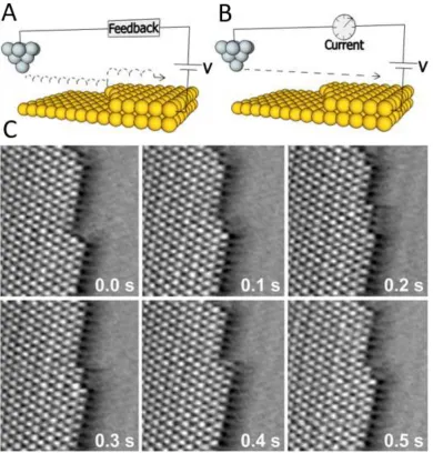
separation. Most commonly, STM is operated in a “constant current” mode (see Figure 6A),
where the measured current is kept constant by adjusting the position of the tip. During
operation, the z-positional adjustment is measured as the tip is scanned across the sample,
allowing maps of the sample topography to be produced. It should be noted that care must be
22 density of states and not just tip-substrate distance (i.e., topography). In comparison to
alternative newer in situ methods, such as electrochemical liquid cell TEM,138 there has been
something of a decline in interest in EC-STM. However, recent innovations which we consider
here, should rekindle interest and lead to the increased use of EC-STM.
4.2 Combined Voltammetry and EC-STM Studies
A key attribute of in situ EC-STM is the ability to track changes in surface topography during
voltammetry. Although this is a well-known use of EC-STM, several recent studies illustrate
the considerable information that can be obtained. As an example, the potential dependence of
anion intercalation into HOPG in 4 different acidic electrolytes (HCl, HClO4, H2SO4 and
H3PO4) has been investigated.139 At oxidizing (positive) potentials, anion intercalation in
HClO4 and H2SO4 were shown to result in the formation of surface “blisters”, not observed in
the other electrolytes. The first stages of the intercalation involved the erosion of terraces,
locally damaging the surface via formation of holes, new edges, terraces and vertices. This
study also demonstrated how the intercalation process may limit the quality and size of
exfoliated graphene sheets, due to progressive damage to the surface.139 The potential
dependence of germanene growth on Au(111) showed that initial deposition occurred at defects
in the well-documented Au(111) herringbone reconstruction. This structure was then relaxed
by further growth in the troughs of the face-centered cubic surface. Finally, any further growth
created a second layer of small, weakly bound islands before further lateral growth.140
In situ EC-STM has considerable potential for examining energy materials. The oxygen
reduction reaction (ORR) catalyzed by iron-pthalocyanine (FePc) layers adsorbed on Au(111)
was recently studied using EC-STM, 141 with images suggesting the formation of the FePc-O2
complex. The electrochemical roughening of a Pt(111) surface when potential-cycled (between
0.05 V and 1.35 V vs. the reversible hydrogen electrode, RHE) in HClO4 media has also been
elucidated with EC-STM, with the potential held in the double layer region (0.4 V vs. RHE) to
record a series of STM images as a function of the number of cycles, in order to track
morphological changes (“roughening”) induced by oxide formation/stripping. Two different
roughening regimes were identified, a “nucleation and early growth” regime followed by a
“late growth” regime. The first stage showed the formation of an increasing number of
nanoscale islands, which increased in radius and slightly in height with potential cycling.
Interestingly, while the step sites created during the early regime contributed to the surface
23 commenced once the islands coalesced, resulting in island growth in predominantly the
z-dimension (height), which contributed strongly to the voltammetric signal and continued up to
at least 170 voltammetric cycles.142 A follow up study from the same group used
electrochemical – AFM to study the same process but on polycrystalline Pt. The use of this
technique allowed for a wider potential window to be applied (0.05 – 2.5 V), as EC-STM
normally has an upper limit of 1.3 V (extensive oxide film formation) due to conductivity
requirements. The wider potential window used and the polycrystalline nature of the sample
led to a different roughening mechanism. The roughening up to 1.5 V previously observed was
not seen (possibly due to the polycrystalline nature of the sample, as well as the reduced
resolution of the AFM), but the surface was instead roughened above 1.8 V through the
formation of PtNPs.143
A combined ultrahigh vacuum (UHV)-electrochemistry set-up has been developed that
facilitates the preparation and structural characterization of complex nanostructured electrode
surfaces under UHV by STM, and electrode transfer under clean conditions for electrochemical
measurements in a flow cell, including the provision for differential electrochemical mass
spectrometry measurements and the use of collector electrodes to allow product analysis. This
set up was employed to demonstrate the differences in electrochemical (electrocatalytic)
properties in two systems: ORR on PtxAg1-x/Pt(111) monolayer surface alloys and bulk CO
oxidation on Pt monolayer island modified Ru(001) surfaces. In both cases,
potential-dependent surface restructuring (traced with STM), altered the electrochemical signal and
electrocatalytic properties.144
4.3 High Speed STM
While several factors impact the speed at which STM images can be acquired, the limiting
factor is generally the feedback used for “constant current” mode imaging (Figure 6A). While the “constant height” mode (Figure 6B) is only effective on very flat samples and contrast will
be lost in any areas beneath the main imaging plane, it can be carried out much faster than
imaging in the conventional constant current mode.145,146
Recently, high-speed (constant height) EC-STM was utilized to image the surface
dynamics of Au(111) crystals in three different ionic liquids. Each STM frame was obtained
on a timescale of ca. 100 ms, allowing atomic scale changes in the surface to be traced on the
electrochemical timescale. Potential sweeps of the surface showed that for all three ionic
24 (imidazolium and pyrrolidinium cations explored). Near the potential of zero charge, interfacial
ions are highly mobile, but when the potential was swept cathodically a sequence of ordered
adlayers was observed. Cations adsorbed parallel to the surface formed a first stripe-like phase,
and as the potential was reduced further an almost square in-plane structured adlayer was
formed.145 A study from the same group investigated the microscopic mechanisms of Bi
electrodeposition on Au(111) and Au(100) surfaces. Using high-speed STM, real time videos
of atomic movement were obtained, in which Bi-Bi bond formation was shown to govern the
epitaxial growth of the Bi deposits in an electrochemical environment, as shown in Figure 6C.
This study also demonstrated the (electrochemical) formation of truly one dimensional Bi
nanowires on the Au(111) surface.146
[image:25.595.111.502.299.708.2]25
(B) Constant height imaging mode used in (C), where the vertical position of the tip is kept constant and the tunneling current is measured. (C) Sequence of STM images taken in 100 ms intervals of Bi deposits on a Au(100) surface. Atomic resolution of kink propagation along the
island edge is displayed. Scan range of (75 70 Å2). (C) was reproduced from Matsushima,
H.; Lin, S. W.; Morin, S.; Magnussen, O. M. Faraday Discuss. 2016, 193, 171-185 (Ref 146),
with permission from the Royal Society of Chemistry.
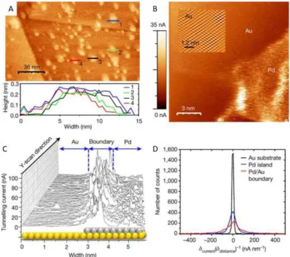
4.4 STM Faradaic Noise Analysis
Faradaic currents are minimized at the STM tip in order to improve the signal-to-noise in
EC-STM images, however, if analyzed appropriately, it has been shown that the faradaic noise in
the tunneling current can provide useful information about electrochemical (electrocatalytic)
activity. This approach was demonstrated in a recent pioneering study, where, using a
conventional EC-STM setup, the faradaic noise in the tunneling current whilst scanning a
Pt(111) surface in aqueous HClO4 was monitored and used to derive information regarding the
location of active catalytic sites. It was shown that when the potential of the sample was
changed to a region where HER occurred, locally increased noise levels were observed over
surface features such as steps. The increase in the tunneling current noise was reasonably
attributed to enhanced catalytic activity, which can be explained by the faradaic processes
altering the local solution composition, which in turn affects the tunneling barrier between the
tip and the sample. The same idea was applied to HER at Pd islands of monoatomic thickness
on a Au(111) surface (Figure 7A) and, once again, an increase in noise was observed over the
Pd compared to the Au(111) surface (Figure 7B), in agreement with the relative HER activities
of these materials. More interestingly, greater tunneling current noise was observed at the
boundary between the Pd islands and Au(111) surface (Figure 7C and D), attributed to a greater
catalytic activity at the boundary, suggesting that maximizing Pd boundary atoms could
increase the macroscopic catalytic activity of the system. Whilst not completely quantitative,
this novel approach has demonstrated the ability of conventional EC-STM to elucidate the
relative contributions of different surface active sites to the overall catalytic activity of
26
Figure 7. (A) In air STM scan of Pd islands on an Au(111) surface with line profiles to display monoatomic height. (B) Constant height STM image of Pd island and Au surface boundary under HER conditions (0.1 M H2SO4). Inset of atomically resolved Au surface via fast Fourier
transform analysis. (C) STM line scans from B, showing increased noise and hence catalytic activity over the first few Pd atoms of the Au-Pd boundary. (D) Statistical current derivatives of STM line scans in C, displaying increased noise over the Pd island and a further increased noise over the Pd/Au boundary. Reprinted with permission from Springer Nature: Nature (Ref
147) (Direct instrumental identification of catalytically active surface sites) by (Pfisterer, J. H.
K.; Liang, Y.; Schneider, O.; Bandarenka, A. S.), COPYRIGHT (2017).
5. Hybrid SEPM Techniques
Above, we have considered some of the key developments in SECM, SICM and EC-STM that
have enabled these techniques to address electrochemical interfaces at the nanoscale. Each
27 combine the merits of different SEPMs and SPMs to provide a more holistic view of interfacial
structure-properties-activity.
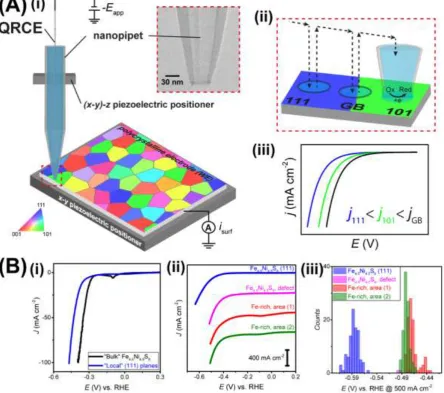
5.1 SECM-SICM
Of the hybrid SEPM techniques, the combination of SECM and SICM, termed SECM-SICM
(or SICM-SECM),88,97 is particularly powerful. Most commonly, probes suitable for
SECM-SICM can be constructed using a dual-barreled theta pipet, with one open channel for precise
tip positioning and topographical mapping using SICM feedback, and the second channel
containing a solid electrode for SECM sensing (Figure 8A-i).70
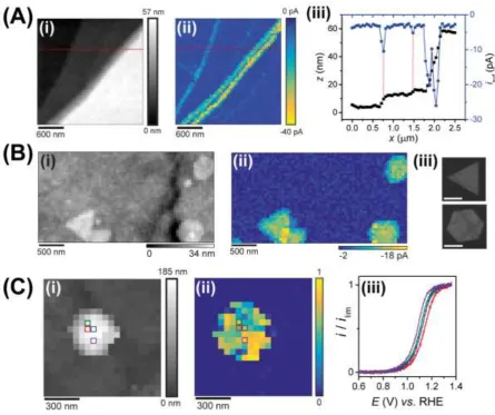
The considerable capability of SECM-SICM is demonstrated by mapping of topography
simultaneously with molecular uptake across the cell wall of living Zea mays root hair cells
(Figure 8A-ii and 8A-iii).148 The SICM channel was used to both map topography and deliver
a target molecule of interest, [Ru(NH3)6]3+, by loading the tip with [Ru(NH3)6]3+ and applying
a positive tip bias to promote delivery. The corresponding uptake was quantified by
amperometric detection of [Ru(NH3)6]3+ at the SECM channel (by diffusion-limited reduction).
A key aspect of this study was the use of a self-referencing strategy, in which the response of
both the SICM and SECM channels were updated in bulk solution at each pixel in images that
were obtained in a hopping mode (see Figure 3C). This was particularly important for the
SECM channel because, in common with many amperometric electrodes employed for cellular
analysis, its response deteriorated during the course of a scan, but this could be fully accounted
for by referencing the near surface SECM current to the corresponding updated value for bulk
solution. With this approach, uptake can be monitored quantitatively, because as the
SECM-SICM probe is approached towards a sample, into which the species, [Ru(NH3)6]3+, can pass
from the SICM channel, there is a decrease in the electrochemical signal at the SECM channel
compared to that in bulk solution (SECM tip detection in competition with cellular uptake). In
contrast, over an inert sample (i.e., an impermeable surface), there is an increased current at
the SECM channel, as the mass-transport from the open (SICM) channel becomes restricted,
compared to when the probe is in bulk solution, and a higher flux results at the amperometric
electrode. Enhanced uptake rates were measured at the tip of the cells, where the SECM current
was lower (Figure 8A-iii). It is interesting to note that differences in cellular uptake between
the tip and body of Zea mays root hair cells correlated with surface charge variations previously
28 SICM-SECM has been utilized further, combining the ionic and electrochemical
currents recorded at the dual-channel probe, to infer on the spatial ion concentration profile and
chemical fluxes, around either an unbiased electrode or near a cell membrane.149 For the
substrate electrode case, this approach allowed the kinetics of redox mediator regeneration to
be probed. In the case of cell imaging, heterogeneous permeability of and adipocyte cell
membrane to ferrocene methanol (FcCH2OH), a hydrophobic redox-active probe molecule that
can hence cross the membrane, could be observed. The SECM probe was held at a potential to
drive the oxidation of FcCH2OH and so could be used as a measure of the local FcCH2OH
concentration.
5.2 AFM-SECM
AFM has been effectively coupled with other techniques to produce multifunctional
capabilities for high-resolution imaging.47 The coupling of AFM and SECM was reported
almost 2 decades ago,150,151 and tips and instrumentation for AFM-SECM are now available
commercially, which should increase the number of groups using this technique and diversify
applications. Using specially designed SECM-AFM cantilever tips electrochemical,
topographical and mechanical information of the substrate can be acquired simultaneously.
152-154 Such a hybrid approach, relying on the capability of SECM for probing the electroactivity
(or chemical fluxes) and of AFM for topography and substrate mechanical properties, can be
extremely useful for investigating soft electronic devices, such as implantable and wearable
electrodes or flexible lab-on-a-chip devices.155
A design that incorporates a conical nanoscale electrode on the end of an AFM tip has
recently been introduced, thoroughly characterized, and applied to several systems to highlight
the versatility of AFM-SECM imaging,153,156 including mapping electrochemistry of outer
sphere redox reactions at HOPG, where high activity of the basal plane was observed, in line
with macroscopic157 and nanoscopic measurements from other electrochemical imaging
techniques.158 Conical tips have also being employed for imaging, with high spatial resolution,
the flux of [Ru(NH3)6]3+ through silicon nitride nanopore arrays with different pore-pitch
spacing allowing the in situ visualization of the radial diffusion across the nanopores and how
pore pitch can impact the diffusion profiles at the nanoscale.159 50 nm radius Pt disk electrodes,
attached to quartz tuning forks, have been used as AFM-SECM tips and employed for the
29 substrates. The geometry of these tips (much closer to a conventional SECM electrode)
facilitates the quantitative analysis of the electrochemical response.160
Despite an apparently small trade-off in resolution when compared to the highest
standalone SECM studies employing nanoscale-sized electrodes, it is clear that the integration
of SECM with AFM brings a clear advantage over SECM alone, as it neatly solves the
topography/activity conundrum, mentioned above in Section 2.1, and allows a much greater
diversity of substrate topography to be tackled than possible with SECM constant height
imaging. Not surprisingly many standalone applications of AFM or SECM are now being
revisited with AFM-SECM. Corrosion processes, for instance, can now be accessed in situ by
monitoring both topographical changes on the substrate and by electrochemically detecting
oxidation products of the corrosion process and/or substrate passivation, providing deeper
insight on the corrosion process.161
The use of AFM in tandem with SECM allowed AFM-SECM to be employed as a
read-out of microarray-based sensing systems. Such devices are often employed for important
biological screenings (such as enzyme-linked immunosorbent assay) and often rely on
fluorescence techniques as read-out. Despite the high sensitivity, the lateral resolution of
fluorescence read-out is diffraction-limited. By employing molecule touching-AFM,162 where
the tip is functionalized with redox active molecules, rather than the redox molecules being in
solution, AFM-SECM has been used as a high throughput serial read-out technique for imaging
high density molecular nanoarrays.163 Owing to the flexible chemical detection capabilities of
SECM, many applications of AFM-SECM as a bioanalytical sensing tool or in the study of
biologically relevant samples have being reported, such as screening immunocomplexes
anchored to single viral particles,164,165 and investigations of the insertion of protein pores into
supported lipid membranes, an important cell membrane model.166 AFM-SECM (and its
diverse modes of operation) will undoubtedly find further use on biologically relevant samples
(much like SECM-SICM, described in Section 5.1) especially considering further efforts
towards the development of AFM-SECM capability, such as conductive colloidal probes
recently reported.167
AFM-SECM and conducting AFM tips will be employed increasingly to probe the
activity and function of energy materials. There was a very interesting recent report on the
direct, in operando, measurement of the electrochemical potential of electrocatalysts, by using
30 topographical and volume changes in energy materials during operation is a very powerful
application,169 and one can envisage how these types of study would be further enhanced with
AFM-SECM.
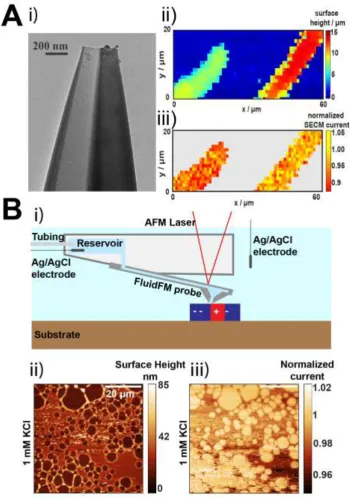
5.3 AFM-SICM
A recent AFM-SICM hybrid technique using a commercial AFM probe (for topography) with
a fluid channel for conductance measurements has been implemented for high speed charge
mapping (Figure 8B-i).170 This approach uses the force based feedback of AFM for mapping
topography, whilst simultaneously recording the ionic current through the open pore of the
AFM tip (as in SICM) to infer on surface charge (Figure 8B-ii and 8B-iii). The approach builds
on earlier applications of the so-called Fluid-Force Microscopy (FluidFM) technique for
simultaneous AFM-SICM measurements.171,172 This approach shows great promise for
mapping surface charge at “hard” materials and speeds up the image acquisition process
compared to present SICM charge mapping methods (Section 3.3.1). More work is needed to
determine whether this approach can be extended to soft, living systems, without causing
sample damage, and whether small orifice sizes that compete with the 30 nm presently
achievable with SICM will be possible in AFM-SICM.119 This hybrid approach has also been
employed to modify substrates in a nano-fabrication approach where the chemical-solution
delivery capabilities of SICM116,173 are combined with the topographical sensing capabilities
of AFM to “print” patterns and structures over the substrate surface in a very precise and