Research on Grain Detection of Grain-Oriented Silicon Steel Based
on Two-Dimensional X-Ray Diffraction
Li Xiao-ning
1,2, He Fei
1,*and Xu Ke
11Collaborative Innovation Center of Steel Technology, University of Science and Technology Beijing, Beijing 100083, China 2Institute of Engineering Technology, University of Science and Technology Beijing, Beijing 100083, China
In order to improve the electromagnetic properties of transformer cores, grain size and boundaries detections of grain-oriented silicon steel are necessary. Conventional electron microscopic grain size detection is off-line and destructive, which cannot meet the requirements of modern production. X-ray detection is non-destructive and the sample can be dynamic. In this paper a new method of the grain boundaries de-tection of the Hi-B grain-oriented silicon steel with large grains has been proposed based on the change of images capturing by the two-di-mensional X-ray diffraction system. The grain boundaries map is calculated with diffraction information which is extracted from the images based on a series of image processing algorithms. The results are basically consistent with the electron microscopy. Compared with the tradi-tional method, the dynamic and non-destructive detection method is able to increase the detection efficiency and improve the overgeneraliza-tion of sampling. Compared with X-ray diffracovergeneraliza-tion contrast tomography, this method is more efficient and low-cost. The sample can also be used after the detection, especially in high-end applications. When the grain boundaries are determined, the necessary processing method can be adopted to further enhance its electromagnetic performance in subsequent processing. [doi:10.2320/matertrans.M2017252]
(Received August 10, 2017; Accepted December 28, 2017; Published February 25, 2018)
Keywords: grain boundaries, two-dimensional X-ray diffraction, non-destructive detection, grain-oriented silicon steel
1. Introduction
Grain-oriented silicon steel is the most important soft magnetic material used as core material of transformers1).
The material is manufactured through many complicated steps, leading to such electrical steel product being honored as an artistic product of iron2,3). The commercially
import-ant properties are the high permeability and low core loss at a high electromagnetic induction. The core loss consists of hysteresis loss and eddy-current loss6,7). Its magnetic
proper-ties are closely related to the sharpness of the secondary re-crystallization texture, especially {110}<001> (Goss tex-ture)4,5). The Hi-B (high-permeability grade) is an important
product with sharp Goss texture accounting for more than 85% of the volume, which makes it as a great magnetic ma-terial8). Usually the sharpness can be detected by using
stacks of slices9). So in this paper, the aim is not the texture
sharpness but the difference between adjacent grains. In order to reduce the core loss, two ways had been ap-plied in processing previously. One is improving
{110}<001> alignment and the other is reducing the thick-ness of silicon steel sheet. But these ways are more and more difficult with the development of production technol-ogy. Adjusting the magnetic domain structure can also achieve the purpose of reducing core loss. The grain size in the product of Hi-B is so large (10 30 mm), resulting in large magnetic domains, which give rise to a large eddy-cur-rent loss as the domain walls move back and forth under the action of alternating field10). In recent years, it has been
studied extensively to decrease large eddy-current loss, and a number of techniques have been developed. Laser or other mechanical methods can refine of the magnetic domain ef-fectively, if the grain boundaries can be detected and determined11–13).
There have been some methods for detecting grain size
and boundaries, such as metallurgical microscope, electron backscatter diffraction(EBSD)14), Transmission electron
mi-croscope15), scanning electron microscope(SEM)16),
laser-ul-trasonic measurement17). But these methods have many
dis-advantages. Some of the traditional methods are destructive because the sample need to be polished before testing. Others can only obtain the average grain size without grain boundaries.
X-ray diffraction has been widely used in texture analy-sis18). Poly19) or monochromatic20) synchrotron X-ray
sources and polychromatic laboratory X-ray sources are ap-plied to different methods of detection. In the 1990s, the two-dimensional X-ray diffraction detector diffraction sys-tems was designed and now have been used in texture and residual stress detection21,22). Pole figure can be calculated
from the data of X-ray diffraction. X-ray diffraction contrast tomography (DCT) has been used to map the grains orienta-tions in 3D23). These methods are accurate enough and
in-creasing applied in the field of material testing and charac-terization, but it is difficult to apply in the field of production monitoring because of the cost and the complexity. Compared with electron backscatter diffraction and metallo-graphic methods, X-ray is non-destructive for the sample and efficient. Compared with one-dimensional X-ray dif-fraction, two-dimensional X-ray diffraction has the charac-teristics of high-speed and large data volume, which can im-prove the detection speed and be expected to be used for online detection24). The average grain misorientation of Hi-B
oriented silicon steel is about 3 degrees13), therefore
orienta-tions of different grains lead to a change of the diffraction images. In this paper, two-dimensional X-ray diffraction system was built to obtain the images. The different images depending on the misorientation can be used to calculate and identify the different grains. The grain map containing the information of grain size and grain boundaries can be pro-duced with image processing methods. The reliability of the detection method is verified by metallographic results. * Corresponding author. E-mail: [email protected]
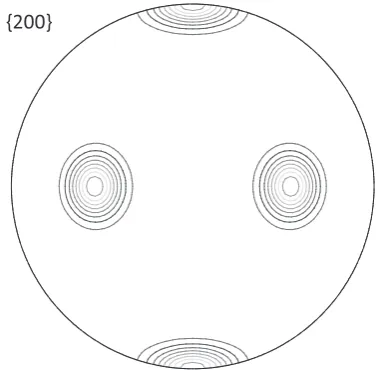
chromatic X-ray, the diffraction pattern is produced as a se-ries of cones with different θ. As shown in Fig. 1(a), differ-ent cones can be calculated to get differdiffer-ent pole figures. With the change of the χ and ϕ, the pole figure as shown in Fig. 1(b) can be efficiently detected by two-dimensional detector.
Hi-B grain-oriented silicon steel is polycrystalline mate-rial with Goss texture, so in order to obtain the grain size and boundaries. If the diameter of X-ray is small enough, the result of the diffraction received by detector is usually one or several spots.
2.2 Diffraction System
Grain boundaries dynamic detection system based on two-dimensional X-ray diffraction is shown in Fig. 2. The equipment is D8 discover from BRUKER with the detector vantec500, and the software is DIFFRAC.SUITE. But the mechanical structure and the platform was redesigned27).
The m in Fig. 2(a) is related to different material and
calcu-plane. The lifting device numbered as 8 makes it possible to detect the samples with different thicknesses effectively.
2.3 Principle of Grain Boundaries Detection
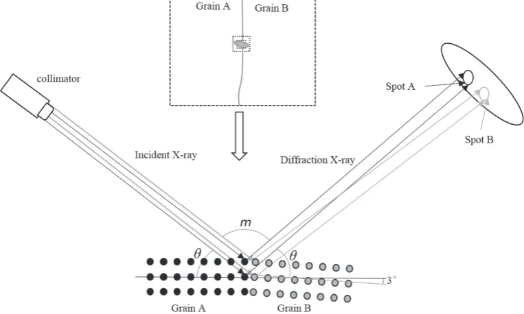
X-ray is generated and goes through the collimator. And then the sample is irradiated with the X-ray. The diffraction information can be received by the two-dimensional detector as shown in Fig. 4. The sample platform moves along the x and y axes, and diffraction measurement is performed at each step. Due to the tiny misorientation, the change of dif-fraction spot position indicates that there are different grains.
Fig. 1 Schematic of two-dimensional data collected by the area detector (a) X-ray diffraction diagram (b) Detection angle of X-ray correspond-ing to the texture position.
Fig. 2 Mechanical structure of online detection system for micro structure of material 1̶Half circle stent; 2̶Mobile bar; 3̶Rail; 4̶X-ray detector; 5̶X-ray sources; 6̶Rotation axis; 7̶Sample platform; 8̶Lifting appliance; 9̶X-ray.
[image:2.595.330.519.419.604.2] [image:2.595.49.292.517.596.2] [image:2.595.137.461.656.760.2]The working voltage of X-ray diffraction system is 35 kV, and the current is 40 mA. The diameter of collimator is 1 mm. Because the sample is irradiated with X-ray obliquely, the sample area involved in the diffraction is ellip-tical as shown in Fig. 5. The angle Ah between X-ray and the
horizontal plane is calculated with θ and q:
Ah=arcsin sinθ×sin π
2 −q (2) Therefore, the angle between y axes and the long axis of an ellipse is:
Ay=arctan tanθ×cos π2 −q (3)
So, the Ah is 26.30 degrees and the Ay is 29.62 degrees.
The long axis of ellipse is 2.26 mm. The long axis direction is not parallel to the direction of x or y direction, and 2.26 mm is decomposed into x and y direction which are 1.12 mm and 1.96 mm. Therefore, the moving step of the electrically controlled rail platform in the direction of x and
y axes is chosen to be 1 mm, which means a diffraction im-age is acquired at an interval of 1 mm. That can ensure the most area can be detected by the X-ray system.
The misorientation is complicated, but the process can be simplified. X-ray is irradiated on grain A, after the sample moving it will be grain B as shown in Fig. 5. Because of tiny misorientation, the angle between crystal planes of the dif-ferent grains lead to difdif-ferent diffraction spots. The spots in images received by detector have different positions and in-tensities which can be calculated to map the grains. The di-ameter of detector is 140 mm, and the distance ld between
[image:3.595.107.489.73.302.2]the sample surface and the detector is 200 mm as shown in Fig. 6. When the angle between two crystal planes is t degrees:
t=θi1−θi2 (4) Where the incident X-ray angle θi1 and the diffraction X-ray
Fig. 4 Diagrammatic sketch of different grain diffraction under X-ray.
Fig. 5 Step selection principle according to the shape of X-ray on sample.
[image:3.595.305.545.347.498.2] [image:3.595.306.550.551.733.2]The resolution of the detector is 2048 × 2048. In order to obtain a good quality image, the diffraction time is set to 3 seconds at each step and then detection sequence is pre-served. Because of the tiny angle of the crystal planes, the received images of different grains are different as shown in Fig. 7.
The diffraction spot position and intensity are obtained af-ter the preprocessing and feature extraction. Each diffraction spot indicates one grain under the incident X-ray. A plurality of spots in the diffraction image means that there are a plu-rality of grains participating in the diffraction, and the dif-fraction area is divided according to the difdif-fraction intensity. When there is no diffraction spot in the image, it means that the grain involved in the diffraction is non-Goss orientation.
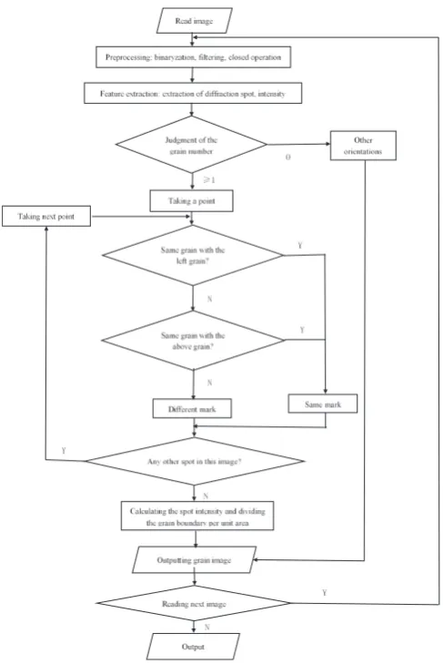
The program of entire processing is designed as shown in Fig. 8, specifically including the following steps:
(1) Read the image and preprocess: Preprocess the image by binarization, then filter the noise by median filtering which selected template is square (8 × 8 pixel). To en-sure that the diffraction spot is a single connected re-gion, the morphological closed operation is performed. The closed operation is on the basis of morphological image processing29), where dilation (⊕) and erosion (⊖)
are applied in order:
X·S =(X⊕S) S (7) Where X is original image, S is the structuring element. The center point of the diffraction spot in the figure rep-resents the position of the current diffraction spot, and the intensity information in the diffraction spot area is
which indicates that the diffraction grain has changed. (5) Generate grain map: According to the above process and
the results of each diffraction, the grain map of the cur-rent sample is given, and diffecur-rent grains are marked with different colors.
3. Experiment and Analysis
3.1 Experiment
The samples used in this experiment were 0.3Q21G Hi-B
Fig. 7 The actual diffraction results of grain-oriented silicon steel of
[image:4.595.49.290.646.761.2]grain-oriented silicon steel sheet. Detection was finished with the two-dimensional X-ray diffraction system, and the system parameters was introduced in section 2. The experi-ment was conducted offline and the data were processed by the program after all the images were collected.
In the metallographic experiment, the samples were pol-ished by 2000# sandpaper until there was no scratch on the surface. The steel sheet is 0.3 mm thick and inorganic coat-ing is about 3 μm thick. The coating should been polished off to make the erosion easily. After the sample was soaked with 4% hydrochloric acid alcohol solution for thirty min-utes, the grain and grain boundaries were obviously observed.
3.2 Experimental Results
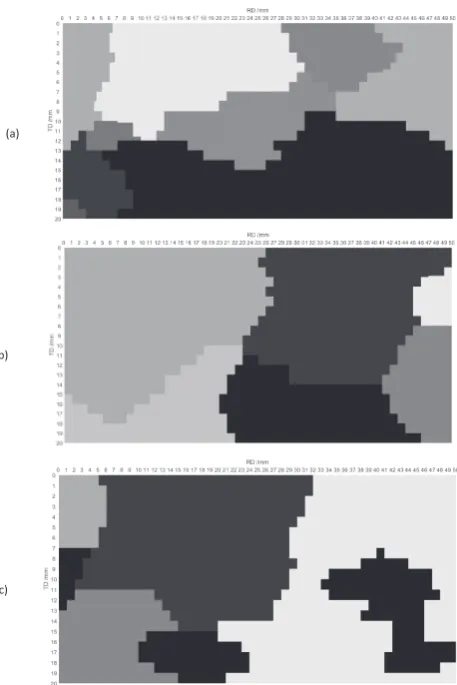
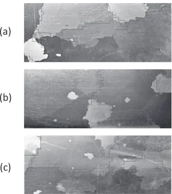
A lot of samples were detected by two-dimensional X-ray diffraction system. There are the similar results. Three typi-cal samples (a), (b), (c) are showed here. After processing, the grain boundaries results are obtained in Fig. 10. Different colors represent different grains, but the orienta-tions of the grains are not related to any color. And the black indicates that the diffraction spots are not detected in the dif-fraction images because the orientations of some grains are not Goss texture. The grain size with Goss is about 20 30 mm. Meanwhile, the grain boundaries are approxi-mately in agreement with the metallographic results showed in Fig. 11.
3.3 Analysis and Discussion
(1) In the experiments, some diffraction information of the other orientation cannot be accurately detected due to the position limitation of the detector, but the impact on the detection results is limited which benefits from the sharpness of Goss texture. The diameter of the collima-tor, the moving step of the sample platform and the dif-fraction time also have some influences on the experi-mental results. Therefore, it is necessary to optimize the parameter selection of the relevant conditions compre-hensively in the future.
(2) In Fig. 11, some of the boundaries have not been
de-tected. In the results of diffraction images, there may be some overlapping diffraction spots that cannot be differ-entiated, probably because the orientation of several grains is so similar, or some small spots are covered by big spot. The results should be expressed clearly by us-ing higher precision equipment and advanced image Fig. 9 Specific preprocessing and feature extraction in program.
[image:5.595.115.484.74.262.2] [image:5.595.313.542.306.649.2]processing algorithm.
(3) In the experiment, the accuracy of 1 mm is not sufficient for the accurate detection of grain boundaries where fur-ther improvement is required. And each step the diffrac-tion area on the surface of the sample is overlapped with another step, so the shape of the collimator also can to be adjusted in the future.
4. Conclusions
(1) Based on the principle of two-dimensional X-ray dif-fraction, a non-destructive method for detecting grain size and boundaries of Hi-B grain-oriented silicon steel has been proposed, and dynamic data collection system built in the experiment has satisfied with the detection. The results has been corroborated by traditional metallo-graphic method. The dynamic non-destructive detection can be used in the production and processing of high-end products.
(2) In the method, the moving step precision of the device is 1 mm, and if the grain boundaries are required to be de-tected with high precision, it can be realized by adjust-ing the movadjust-ing step precision, the diameter of the X-ray beam and the time of diffraction synthetically. So in fur-ther research, the misorientation can also be detected ac-curately. Secondly, it is necessary to increase the detec-tor number and ensure that more diffraction information can be obtained. Finally, more refined and efficient im-age processing algorithm is required for dealing with the overlap of diffraction spots, which can improve the ac-curacy of detection, and achieve the goal of high preci-sion online detection.
(3) There are already many advanced equipments can map the grains in 2D or 3D. But the cost and complexity make it difficult to be applied on-line. So the method in
4) N.P. Goss: Trans. Am. Soc. Met. 23 (1935) 511–531.
5) L.F. Fan, S.T. Qiu, L. Xiang and G.B. Tang: Mater. Trans. 55 (2014) 123–127.
6) H. Jung, S.B. Kim, J.B. Kim and J. Kim: ISIJ Int. 51 (2011) 987–990. 7) Y. Ushigami, M. Mizokami, M. Fujikura, T. Kubota, H. Fujii and K.
Murakami: J. Magn. Magn. Mater. 254–255 (2003) 307–314. 8) A. Morawiec: Scr. Mater. 64 (2011) 466–469.
9) M. Frommert, C. Zobrist, L. Lahn, A. Böttcher, D. Raabe and S. Zaefferer: J. Magn. Magn. Mater. 320 (2008) e657–e660.
10) K. Ishiyama, S. Hashi, M. Kawasaki and K.I. Arai: Mater. Trans., JIM
37 (1996) 469–472.
11) M. Imafuku, H. Suzuki, K. Akita, K. Iwata and M. Fujikura: Acta Mater. 53 (2005) 939–945.
12) S.V. Ponnaluri, R. Cherukuri and P.A. Molian: J. Mater. Process. Technol. 112 (2001) 199–204.
13) W.M. Mao and P. Yang: Material Science Principles on Electrical Steels, Beijing, (Higher Education Press, 2013) 375–441.
14) A. Bowles, K. Nogita, M. Dargusch, C. Davidson and J. Griffiths: Mater. Trans. 45 (2004) 3114–3119.
15) K. Fujii and K. Fukuya: Mater. Trans. 52 (2011) 20–24.
16) J. Goldstein, et al.: Scanning Electron Microscopy and X-ray Microanalysis: a text for biologists, materials scientists, and geolo-gists, (Springer Science & Business Media, 2012).
17) Y. Nagatomo, T. Kitahara, T. Nagase, Y. Kuromitsu, H. Sosiati and N. Kuwano: Mater. Trans. 49 (2008) 2808–2814.
18) K. Kashihara and H. Inagaki: Mater. Trans. 48 (2007) 1986–1991. 19) G.E. Ice and J.W.L. Pang: Mater. Charact. 60 (2009) 1191–1201. 20) N. Viganò, A. Tanguy, S. Hallais, et al.: Sci. Rep. 6 (2016) 20618. 21) L. Lutterotti, D. Chateigner, S. Ferrari and J. Ricote: Thin Solid Films
450 (2004) 34–41.
22) O. Takakuwa and H. Soyama: Advances in Materials Physics & Chemistry 3 (2013) 8–18.
23) M. Holler, A. Diaz, M. Guizar-Sicairos, P. Karvinen, E. Färm, E. Härkönen, M. Ritala, A. Menzel, J. Raabe and O. Bunk: Sci. Rep. 4 (2014) 3857.
24) B.B. He, U. Preckwinkel and K.L. Smith: X-Ray Anal 46 (2003) 37–42.
25) B.B. He, U. Preckwinkel and K.L. Smith: X-Ray Anal 43 (2000) 273–80.
26) L. Chen, W.M. Mao, H.P. Feng and Y.N. Yu: Materials Science Forum
408–412 (2002) 227–232.
27) B.B. He: Two-Dimensional X-Ray Diffraction, (2009) pp. 62–63. 28) D. Mainprice, R. Hielscher and H. Schaeben: Geol. Soc. Lond. Spec.
Publ. 360 (2011) 175–192.
29) D. Zhang: Extended Closing Operation in Morphology and Its Application in Image Processing, (2009).
[image:6.595.85.253.68.257.2]