Abstract—The read/write performance asymmetry of Solid State Disks (SSDs) remains a critical concern for read performance. Under a concurrent workload with a mixture of read and write requests, preceding write requests preempt available flash memory resource so as to block read requests, which we call write-caused interference. Hence, the read performance, which is often more critical than the write performance, can be significantly degraded. Unfortunately, state-of-the-art schedulers either are inefficient in improving the read performance or suppress the write performance. In this paper, we propose a novel scheduler at device level, called AOS, to mitigate the write-caused interference and maximize the read performance without sacrificing the write performance. Specifically, AOS designs a conflict detection module, to efficiently identify access conflicts among requests. Then, AOS adaptively dispatches as many outstanding requests as possible to a re-ordering set based on the detected conflicts to reduce the write-caused interference and improve the flash-level parallelism (FLP). Finally, AOS carefully re-orders the dispatched requests to reduce channel-level access conflicts and improve the system-level parallelism (SLP). Extensive experimental results show that AOS reduces, an average of 51% read latency and 45% write latency, compared to FIFO.
Index Terms—out-of-order scheduling, solid state disk, write-caused interference, conflict detector
I. INTRODUCTION
AND flash-based Solid State Disks (SSDs) have been widely deployed in data centers due to higher throughput, lower latency, and lower energy than hard disk drivers (HDDs) [1]. However, SSDs suffer from two critical limitations: the read/write performance asymmetry and the erase-before-write feature. Previous works [2, 3]
Manuscript received December 11, 2014; revised January 20, 2015. This work is sponsored in part by the National Natural Science Foundation of China No. 61300047 and the National Basic Research Program of China (973 Program) under Grant No.2011CB302303。
Pingguo Li is with the Wuhan National Laboratory for Optoelectronics, Huazhong University of Science and Technology, Wuhan 430074, P.R. China, and the Library, Hubei University of Science and Technology, Xianning 437000, P.R.China ( e-mail: [email protected])
Fei Wu is with the Wuhan National Laboratory for Optoelectronics, Huazhong University of Science and Technology, Wuhan 430074, P.R. China (phone: 0086-27-87792405; fax: 0086-27-87792405; e-mail: [email protected]).
You Zhou is with the Wuhan National Laboratory for Optoelectronics, Huazhong University of Science and Technology, Wuhan 430074, P.R. China (e-mail: [email protected]).
Changsheng Xie is with the Wuhan National Laboratory for Optoelectronics, Huazhong University of Science and Technology, Wuhan 430074, P.R. China (e-mail: [email protected])
Jiang Yu is with the IBM China System and Technology Group Lab,
Shanghai 200000,P.R.China (e-mail: [email protected])
show that, under a concurrent workload with a mixture of read and write requests, the read performance can be significantly degraded, since preceding writes requests preempt available flash memory resource and block read requests. Note that the write operation of flash memory is much slower than the read operation. To make the matter worse, if the block to be written is not free, an erase operation, which is much slower than the write operation, must be performed before serving the write request due to the erase-before-write feature, further degrading the read performance. We refer to the read performance degradation as the write-caused interference. Unfortunately, the read performance is often more critical than the write performance [4], it is necessary to mitigate the write-caused interference. In order to achieve this, some studies on SSD I/O schedule are proposed at operating system level. Wang et al. [5] attempted to divide incoming read/write requests into different sub-regions, and then served them in a round-robin manner. Gao et al. [6] dispatched requests to different batches based on an access conflict detection approach to avoid access conflicts. Although these works achieve some optimizations in reducing the write-caused interference, the optimizations are purely based on the logical page addresses (LPAs) required by the file system. Since the same LPA is always redirected to different physical page addresses (PPAs) due to the out-of-place write strategy of SSDs [2, 3], the optimizations cannot be efficient and accurate. To avoid these drawbacks, Wu et al. [7] proposed a P/E (program/erase) suspension, a device-level scheduler, to reduce the write-caused interference. However, frequently suspending/resuming the on-going P/E operation introduces system overhead and suppresses the write performance. In addition, this method required hardware modification.
In this paper, we propose AOS, a novel device-level scheduler, to mitigate the write-caused interference and maximize the read performance without sacrificing the write performance. This paper makes the following contributions:
We proposed a conflict detection module to identify access conflicts among requests.
We proposed an adaptive request dispatching policy to dispatch as many outstanding requests as possible to a re-ordering set to reduce the write-caused interference and improve the flash-level parallelism (FLP). Our experiments show that this policy reduces an average of 55% write-caused interference and improves FLP by about 2 times over FIFO under enterprise workloads.
We proposed a re-ordering policy, which reorders the dispatched requests in a round-robin manner to reduce channel-level access conflicts and improve the system-level parallelism (SLP). Our experiments show that this policy reduces an average of 31% channel-level access conflicts and
AOS: Adaptive Out-of-order Scheduling for
Write-caused Interference Reduction in Solid
State Disks
Pingguo Li, Fei Wu*, You Zhou, Changsheng Xie, Jiang Yu
improves SLP by about 1.3 times over FIFO under enterprise workloads.
We evaluate AOS with various enterprise workloads. AOS reduces an average of 51% read latency and 45% write latency compared to FIFO. In addition, we show that AOS provides better performance than two state-of-the-art schedulers [6, 7].
The organization of this paper is as follows. In Section II the characteristics of SSDs and out-of-order execution are introduced. The design of our AOS scheduler is presented in Section III. Section IV presents our experimental methodology and results. Section V provides our conclusions.
II.BACKGROUND
A. NAND Flash Memory
A NAND flash memory chip is the basic service unit and has independent chip enable (CE) and read/busy (R/B) singals. Each chip consists of several dies, which has an internal R/B signal and can work independently. Each die is composed of several planes sharing the same wordline and voltage driver. Each plane holds several blocks, and each block contains a number of pages, each of which includes several sectors.
There are three basic operations in flash memory: read, program and erasure. Read and program are typically performed in a page unit, while the erasure is typically performed in a block unit. In general, a program operation is about 10 times slower than a read operation, but about 8 times faster than an erase operation [8].
[image:2.595.48.292.485.573.2]To exploit the parallelism inside chips, three advanced commands including interleave, multiplane and copyback, are supported by flash manufactures, additionally. They enable flash memory operations to be processed in parallel, which we refer to as the flash-level parallelism (FLP). B. Solid State Drives
Fig.1. An illustration of SSD architecture
Fig. 1 illustrates a general architecture of an SSD including a main controller, a set of NAND flash memory chips and a DRAM chip. The main controller is composed of a host interface controller, an embedded CPU with SRAM, a DRAM controller and flash controllers. The host interface controller receives I/O requests from the host and transfers data between the host and the SSD through a specific bus interface protocol such as SATA, SAS or PCI-E. The embedded CPU with SRAM provides computing power for running the software layer, called flash translation layer (FTL). The FTL translates I/O requests to flash requests, specifically, translates logical page addresses of I/O requests, which are used in host system, into physical page addresses, which are used to access flash memory. The FTL also performs garbage collection, and wear leveling operations. Each flash controller, which issues read, program, and erasure commands to NAND flash chips, works
independently. Each flash chip, which connects with a flash controller via a channel bus, can execute read, program and erasure commands independently. The flash requests can be dispatched across multiple flash controllers and channels, which we refer to as channel striping. Further, the flash controller can pipeline the flash requests across multiple flash chips in the same channel, which we refer to as channel pipelining. With channel striping and channel pipelining, which we refer to as system-level parallelism (SLP), flash requests can be served in parallel. The DRAM buffers user data and FTL metadata. The dirty data must be written back to flash memory when it is evicted to make free space for incoming new data.
C. Out-of-Order Execution
Out-of-order execution, which originates in early work by Tomasulo [9], is widely employed in microprocessors [10]. The basic idea is to exploit parallelism of available function units to improve the performance of microprocessors by reordering instructions. Out-of-order execution also can be used in SSDs [11, 12]. Flash requests can be reordered to leverage the internal parallelism inside an SSD to improve the I/O performance. To this end, the data dependence in outstanding requests has to be analyzed first to avoid potential data hazards.
Data hazards can be classified into two types, depending on the sequence of read, program and erasure requests in the queue.
PAR (program-after-read)-A program request tries to program a destination flash page before it is read out by a previous read request. As a result, the read request would return a fault value. This hazard arises from an overwrite request.
EAR (erase-after-read)-An erasure request tries to erase a destination block before all the valid data in the block is read out, leading to data loss. This hazard arises from a garbage collection operation.
The two hazards will not occur in a first-in first-out (FIFO) scheduler, because all requests are executed in FIFO order. In contrast, an out-of-order scheduler must prevent any data fault caused by data hazards.
[image:2.595.307.549.542.648.2]III. AOSSCHEDULER
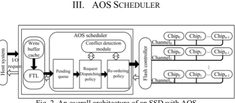
Fig. 2. An overall architecture of an SSD with AOS
Fig. 2 illustrates the overall architecture of an SSD with our proposed AOS scheduler. AOS is designed below the FTL. A write buffer in the DRAM is divided into two regions: a working region, which works as a traditional write buffer, and a dispatching region, which stores the dirty data evicted from the working region. The data in both regions also serve read requests from the host system, which improves read performance.
identifies access conflicts among requests. When a request arrives at AOS, it is inserted into one of the three pending queues, a read queue, a program queue, and an erasure queue, according to its operation type. When the re-ordering set becomes empty, the request dispatching policy adaptively selects a dispatching scheme based on the states of pending queues, and moves as many requests as possible to the re-order set according to the detected conflicts. Then, the re-ordering policy re-orders the requests in the set and issues them to flash controllers until the set becomes empty. A. Conflict Detection Module
Access conflict depends on the locations of requests. If requests go to the same chip at the same time, access conflicts will occur, which we refer to as chip-level access conflicts. To efficiently identify these conflicts, we design a conflict detection module based on request addresses, which consists of four parts: channel, chip, die and plane. A flash request is denoted as follows:
Ri =Ti (channeli, chipi, diei, planei) (1)
Where Ti represents the request type, such as read, program, or erasure, and Channeli, chipi, diei, and planei correspond to channel, chip, die, and plane addresses of flash request Ri.
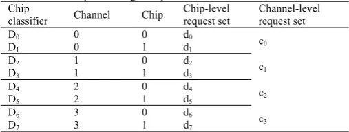
[image:3.595.41.295.575.671.2]The chip-level conflict detection module consists of a set of chip classifiers: D0, D1, …, Dm-1, where m is the number of chips inside an SSD. According to the chip classifiers, we construct a set of corresponding chip-level request sets: d0, d1, …, dm-1. To efficiently identify each chip-level request set, we define a chip-location vector, denoted as vm-1 (dm-1, channelm-1, valid m-1), where channel m-1 represents the channel address of the requests belonging to dm-1, valid m-1 represents whether the chip-level request set is empty. For example, 0 indicates the chip-level request set is empty, and 1 indicates it is not empty. Assume that RS denotes the re-ordering set in the form of RS = {d0, d1, …, dm-1}. Note that each chip classifier composes of two fields: channel and chip addresses. As a result, the total number of chip classifiers equals to the number of chips in an SSD. For example, an SSD has 4 channels, each channel consists of 2 chips, and then the chip-level conflict detection module has 8 chip classifiers as shown in Table 1. According to the chip classifiers, all the requests in the re-ordering set can be distributed into 8 different chip-level request sets.
Table 1 An example with eight chip classifiers Chip
classifier Channel Chip
Chip-level request set
Channel-level request set
D0 0 0 d0 c0
D1 0 1 d1
D2 1 0 d2 c1
D3 1 1 d3
D4 2 0 d4 c2
D5 2 1 d5
D6 3 0 d6 c3
D7 3 1 d7
Formally we define a chip classifier as follows: Dm-1 = (Channelm-1, chipm-1) (2)
A flash request Ri, will be classified into a specific chip-level request set Dm-1 when its channel and chip addresses match the Dm-1’s field values. Specifically, the classification is performed as follows:
Request_c = ((channeli== Channelm-1)&(chipi== chipm-1)) (3)
If Request_c==0, Ri, belongs to Dm-1. AOS successively selects chip classifiers and checks if formula (3) is equal to zero until the chip-level request set is found.
The process of conflict detection is as follows. When receiving a new request, the conflict detection module first identifies which chip-level request set it belongs to based on formula (3). If the valid field of the chip-level request set is 0, there is no access conflict, and then the request is moved directly to the chip-level request set. Otherwise, the chip-level conflict detector further checks whether access conflicts exist and if exist, whether they can be eliminated by die interleaving or multiplane sharing. For example, there are two requests, Ri and Rj, of the same type and they are checked as follows:
Chip_c = ((channeli==channelj)&(chipi==chipj)&(diei==diej)&(planei==planej)) (4)
If Chip_c == 0, there is no access conflict between the two requests. Otherwise, a conflict will occur, and the dispatching operation is cancelled.
B. Adaptive Request Dispatching Policy
To reduce the write-caused interference without sacrificing the write performance, we present an adaptive request dispatching policy, which includes three schemes: read preference dispatching scheme, program preference dispatching scheme and erasure preference dispatching scheme. When the re-ordering set becomes empty, the request dispatch policy adaptively selects one of them to dispatch requests based on the states of pending queue, such as the length of read/program pending queue.
1) Read Preference Dispatching Scheme
If the dispatching region, which dominates the size of program pending queue, is not full, reads are prioritized over programs.
Algorithm 1. Read preference dispatching scheme input: read/program/erase requests;
number_read is the number of read requests; number_program is the number of program requests; number_erase is the number of erase requests.
output: chip-level request sets 1 dim i As Integer
2 while RS is not full and read pending queue is not empty do
3 Picks up a request from the head of this queue. 4 Dispatches it to target dm-1.
5 endwhile
6 if program pending queue is not empty then
7 for i=1 to number_program do
8 if RS is not full then
9 Picks up a new request.
10 If access conflict/data hazard is found then
11 Cancel the dispatching operation. 12 else
13 Dispatches it to target dm-1. 14 endif
15 endif
16 endfor
17 endif
18 if erase pending queue is not empty then
19 for i=1 to number_erase do 20 if RS is not full then
21 Picks up a new request.
22 If access conflict is found then
23 Cancel the dispatching operation. 24 else
25 Dispatches it to target dm-1. 26 endif
27 endif
28 endfor
29 endif
dispatched if the program pending queue is not empty. During dispatching program requests, the chip-level conflict detector will check whether there exists an access conflict between a program request and any other request in the re-ordering set. At the same time, data hazard, such as PAR, must also be checked. Once a conflict/data hazard is found, the dispatching operation is canceled, and then the scheme picks up the next program request. Otherwise, the program request is moved to the corresponding chip-level request set. In this way, we can avoid the write-caused interference. Finally, erasure requests will be dispatched if the erasure pending queue is not empty. Similar to dispatching program requests, access conflicts are also checked. The erasure requests, which do not conflict with any other request in the re-order set, will be moved to the corresponding chip-level request sets.
2)Program Preference Dispatching Scheme
Program requests will be scheduled prior to read requests when the dispatching region is full. Compared to read requests, program requests are less concerned about the response times of individual requests, but they require the scheduler to sustain high throughput.
Algorithm 2. Program preference dispatching scheme input: program/ read/erase requests;
number_read is the number of read requests; number_program is the number of program requests; number_erase is the number of erase requests.
output: chip-level request sets 1: dim i As Integer
2: Do line 7-16 in Algorithm 1.
3: if read pending queue is not empty then
4: for i=1 to number_read do 5: if RS is not full then
6: Picks up a new request. 7: If access conflict is found then
8: Cancel the dispatching operation. 9: else
10: Dispatches it to target dm-1. 11: endif
12: endif
13: endfor
14: endif
15: Do line 18-29 in Algorithm 1.
Algorithm 2 shows the pseudocode of the program preference dispatching scheme. When the dispatching region is full, the service of program requests prioritizes read service to avoid write pipeline stalls. During dispatching program requests, similar to read preference dispatching scheme, access conflicts/data hazards must be checked. Only the program requests without access conflicts/data hazards are dispatched to corresponding chip-level request sets. As a result, write parallelism is well leveraged, improving the write performance. After that there are still free rooms, and then all the read requests, which have no access conflicts with other requests in the re-ordering set, are moved to the corresponding chip-level request sets. During dispatching read requests, access conflicts will be checked to avoid resource competition with other program requests in the re-ordering set. In this way, we can process program requests as soon as possible to avoid write pipeline stalls. Lastly, the erase requests, which have no access conflicts with other requests in the re-ordering set, are moved to the corresponding chip-level request sets if they still have free spaces.
3) Erase Preference Dispatching Scheme
In general, an erasure operation should be avoided until free blocks are not enough or the read and program pending queues are empty. However, it is feasible for an SSD to perform an erasure operation ahead of time if it does not block a read/program request. In this way, the scheduler can efficiently utilize flash memory resources.
Algorithm 3 shows the pseudocode of the erase preference dispatching scheme. When the read pending queue is empty and the dispatching region is not full, erase preference dispatch scheme is adopted. After all the erasure requests are moved to the corresponding chip-level request sets in the re-ordering set, program requests will be scheduled if the program pending queue is not empty. During dispatching program requests, similar to read preference dispatching scheme, only the program requests without access conflicts/data hazards can be dispatched to the corresponding chip-level request sets.
Algorithm 3. Erase preference dispatching scheme input: erase/program requests
number_program is the number of program requests; number_erase is the number of erase requests.
output: chip-level request sets 1: dim i As Integer
2: Do line 19-28 in Algorithm 1. 3: Do line 7-16 in Algorithm 1.
C. Re-ordering Policy
With the chip-level conflict detection module and the adaptive request dispatching policy, the requests are distributed into the corresponding chip-level request sets, according to their operation types, thus the write-caused interference is eliminated. However, channel-level access conflicts may still occur among the requests in different chip-level request sets due to competing for the shared channel resources. To reduce these conflicts, we present a re-ordering policy, which includes constructs the channel-level request set and re-order the requests in the set.
Based on channel addresses of flash requests, we construct a set of channel-level request sets: c0, c1,…, cn-1, each of which consists of a set of corresponding chip-level request sets and is an element of the re-ordering set, which is denoted as RS = {c0, c1, …, cn-1}. For example, an SSD has 4 channels, each channel consists of 2 chips, and then there are 4 channel-level request sets, each of which has 2 chip-level request sets, as shown in Table 1. For two different chip-level request sets, if their channel fields are the same, they will be distributed into the same channel-level request set. For example, the channel fields of v0 and v1 are 0, the corresponding chip-level request set d0 and d1 are distributed into the same channel-level request set c0, denoted as c0={d0 , d1}.
In order to fairly and efficiently reorder the requests in a channel-level request set, the re-ordering policy sets a priority level for each chip-level request set. All the chip-level request sets are in the same priority level of 0 at the beginning of reorder.
round-robin manner until the re-order set becomes empty; (3) selecting a chip-level request set with the lowest priority level in the channel-level request set, and dispatching the requests to the corresponding flash controller. If they are program/erase requests, AOS deletes the chip-level request set after the dispatching is completed. If they are read requests, requests without access conflicts will be issued to the target flash controller. After that if there are still read requests, the priority level of the chip-level request set is increased by 1. Otherwise, AOS deletes the chip-level request set; (4) continuing with step 2 and 3 until all the requests have been dispatched to the corresponding flash controllers.
IV. EVALUATION METHODOLOGY A. Experiment Setup
1) Simulator
We built an event-based trace-driven SSD simulator by adding a scheduling layer into the SSDsim [13]. We implemented the following schedulers in SSDsim simulator: 1) FIFO, 2) PIQ [6], 3) P/E Suspension [7], and 4) AOS. 2) Workloads
We use a set of traces for experimental evaluation, which are collected from actual enterprise applications and are available in [14] and [15]. They include corporate mail server (EX), online transaction processing (FIN), and MSN file server (MSN).
B.Evaluation 1) Latency analysis
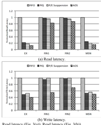
Fig. 3(a) shows the normalized read latencies of the four scheduling policies for all the workloads, compared to FIFO. On average, AOS reduces the read latency by 51%, compared to FIFO. Our best-case read performance comes from EX workload, where we reduce the read latency by 87%. Our worst-case read performance occurs when running FIN2 workload.
(a) Read latency.
[image:5.595.323.527.292.528.2](b) Write latency. Fig. 3. Read latency (Fig. 3(a)), Read latency (Fig. 3(b))
We note that the reduction in read latency does not lead to write performance degradation. Fig. 3(b) shows the write
latencies normalized to that of FIFO. On average, AOS reduces 45% write latency over FIFO.
We also note that the read performance of P/E Suspension is lightly less than that of AOS, an average of 8%, under all the workloads. While P/E Suspension gives read requests the highest priority and serves them as soon as possible by suspending P/E requests, read performance highly depends on the frequency and cost of suspension P/E. Moreover, we find that its write performance is worse, an average of 22%, than AOS. One reason is that P/E Suspension simply postpones write operations, increasing write latency. Another reason is that P/E Suspension cannot efficiently exploit the write parallelism, leading to further write performance loss. 2) Access Conflict Analysis
As described in previous sections, access conflicts are classified into two types: the chip-level access conflicts and the channel-level access conflicts. For the chip-level access conflicts, we only consider the read-blocked-by-write situation. As a result, it refers to the write-caused interference.
(a) Write-caused interference.
(b) Channel-level access conflict.
Fig. 4. Write-caused interference (Fig. 4(a)), channel-level access conflict (Fig. 4(b)).
Fig. 4(a) plots the result of write-caused interference normalized to FIFO. On average, AOS reduces write-caused interference by 55% compared to FIFO under all the workloads.
Fig. 4(b) shows the normalized number of channel-level access conflicts occurred in each scheduler, compared to FIFO. We can see that AOS significantly reduces the channel-level access conflicts, an average of 31%, compared to FIFO.
[image:5.595.65.267.499.749.2]AOS. This is because that the read/write request can be blocked by another read/write request, which has been issued previously.
3) Parallelism Analysis
Fig. 5(a) shows the leveraged FLPs of the four schedulers, normalized to that of FIFO. On average, AOS achieves 2 times of FLPs gains over FIFO under the four workloads. Fig. 5(b) shows the leveraged SLPs of the four schedulers, normalized to that of FIFO. On average, AOS achieves 1.3 and 1.2 times of SLP gains over FIFO and P/E Suspension under the four workloads, respectively, while only 1.08 times over PIQ. This is because, compared to FIFO and P/E Suspension, AOS can make use of channel striping and channel pipelining to maximize the number of active channels and chips. PIQ also deploys a similar re-ordering policy; however, it employs a less efficient dispatching policy. As a result, it degrades lightly in SLP gains over AOS.
(a) FLP (flash-level parallelism).
(b) SLP (system-level parallelism). Fig.5. FLP (Fig. 5(a)), SLP (Fig. 5(b)).
4)Storage overhead
Storage overhead can be categorized into three types: dispatching region, pending queue request entry and re-order set request entry.
Dispatching region: AOS keeps the dirty data evicted from the working region, which adds significant cost. In this paper, AOS requires 2MB of write buffer and the dispatching region size is less 1% of the total DRAM capacity if the size of DRAM is 256MB.
Pending queue request entry: AOS requires three types of pending queues: read, program and erase. We assume there are 512 requests per queue, each request entry has a 64-bit partial physical address stored in it, it consumes 12kB of DRAM capacity.
Re-order set request entry: when the adoptive dispatch policy move requests to the re-order set, corresponding request entries are stored temporarily in DRAM cache before they are dispatched to NAND flash chips, we assume the re-order set can hold 2*n requests, n indicate the number of chip in an SSD and then it consumes 1kB of DRAM capacity if n is equal to 64 and each request entry has a 64 bits partial physical address.
According to the above analysis, the total storage is 2MB +
12KB + 1KB = 2061KB, which is less than 1% of the 256MB DRAM.
V. CONCLUSION
In this paper, we propose AOS, a novel device-level scheduler, to mitigate the write-caused interference and maximize the read performance without sacrificing the write performance. AOS employs a conflict detection module to efficiently identify access conflicts among requests. Then, AOS quickly distinguishes between write requests that will interfere with read requests and those that will not, significantly reducing the write-caused interference. AOS also exploits the write parallelism by postponing the commitments of program requests to the target flash chips, improving the write performance. In addition, AOS further alleviates channel-level access conflicts and improves SSD I/O performance by reordering the dispatched requests. Our experiment results show that AOS reduces an average of 51% read latency and 45% write latency, compared to FIFO.
REFERENCES
[1] N. Agrawal, V. Prabhakaran, T.Wobber, J. D. Davis, M. Manasse, and R. Panigrahy. Design tradeoffs for SSD performance. In Proceedings of the 2008 USENIX Annual Technical Conference, 2008.
[2] S. Park and K. Shen, FIOS: A fair, efficient Flash I/O scheduler, in: Proceeding of the 10th USENIX Conference on File and Storage Technologies(FAST), 2012, pp. 1-15.
[3] J. Ouyang, S. Lin, S. Jiang, Z. Hou, Y. Wang, and Y. Wang, SDF: Software-Defined Flash for Web-Scale Internet Storage System, in: Proceedings of the Nineteenth International Conference on Architectural Support for Programming Languages and Operating Systems (ASPLOS), 2014, pp. 471-484.
[4] S. khan, A. Alameldeen, and C. Wilkerson. Improving cache performance by exploiting read-write disparity. In Proceeding of 20th IEEE International Symposium On High Performance Computer Architecture, 2014
[5] H. Wang, P. Huang et al., A novel I/O scheduler for SSD with improved performance and lifetime, in: Proceeding of the 29th IEEE Symposium on Mass Storage Systems and Technologies (MSST), 2013.
[6] C. Gao, L. Shi et al., Exploiting parallelism in I/O scheduling for access conflict minimization in flash-based solid state drives, in: Proceeding of the 30th IEEE Symposium on Mass Storage Systems and Technologies (MSST), 2014.
[7] G. Wu, P. Huang, X. He, Reducing SSD read latency via NAND flash program and erase suspension, in: Proceeding of the 10th USENIX Conference on File and Storage Technologies (FAST), 2012, pp. 117-123.
[8] K9XXG08UXA datasheet.
http://www.samsung.com/products/semiconductor/flash/technicallinfo/ datasheets.htm, 2014.
[9] R.M. Tomasulo, An efficient algorithm for exploiting multiple arithmetic units, IBM Journal of Research and Development, 1967, Volume 11 Issue 1, pp. 25–33.
[10] G. Hinton, D. Sager, M. Upton, D. Boggs, D. Carmean,A. Kyker, and P. Roussel, The Microarchitecture of the Pentium 4 Processor, Intel Technology Journal, 2001.
[11] S. S. Hahn, S. Lee, and J. Kim, SOS: Software-Based Out-of-Order Scheduling for High-Performance NAND Flash-Based SSDs, in: Proceeding of the 29th IEEE Symposium on Mass Storage Systems and Technologies (MSST), 2013.
[12] M. Jung and M. Kandemir, Sprinkler: Maximizing Resource Utilization in Many-Chip Solid State Disks, in: Proceeding of the 20th IEEE International Symposium On High Performance Computer Architecture (HPCA), 2014, pp. 524-535.
[13] Y. Hu, H. Jiang, D. Feng, L. Tian, H. Luo, and S. Zhang, Performance Impact and Interplay of SSD Parallelism through Advanced Commands, Allocation Strategy and Data Granularity, in: Proceedings of the international conference on Supercomputing (ICS), 2011, pp. 96-107.
[14] UMass Trace Repository, http://traces.cs.umass.edu, 2014.