Implementation of Shortened Pulse Position Modulation
for Optical Communication Systems
Mehmet Sönmez
Osmaniye Korkut Ata University Engineering Faculty, Department of Electrical and Electronics Engineering
ABSTRACT
In this paper, we describe a transmitter scheme which uses Shortened Pulse Position Modulation (SPPM). A modulator based-on hardware is proposed for SPPM technique. The transmitter scheme is designed considering wireless optical communication systems. We use Field Programmable Gate Arrays (FPGA) board to design proposed system. It is shown from simulation results that proposed architecture efficiently generates SPPM signal. Additionally, we implemented on real-time FPGA board since we show that proposed structure has practical scheme.
General Terms
Modulator, Transmitter, Hardware, Software, Algorithm, Optical Communication et. al.
Keywords
Shortened Pulse Position Modulation (SPPM), Field Programmable Gate Arrays (FPGA), wireless optical communication.
1.
INTRODUCTION
For a couple of decades, optical communication systems have been one of the popular issues. Hence, many researchers have improved a lot of proposals for optical communication systems. One of these proposals is the design of new modulator scheme. The PPM, Variable Pulse Position Modulation (VPPM), Variable On-Off Keying (VOOK), Pulse Dual Slope Modulation (PDSM) have been recently proposed for optical communication systems, specifically for Visible Light Communication (VLC) systems. On the other hands, a modulation technique, which is called as Shortened Pulse Position Modulation (SPPM), has been proposed to transmit the image data for the wireless underwater communication systems [1].
There are many papers to provide data transmission for underwater communication systems. One of these papers has been proposed a hardware implementation for underwater communication systems to support the specific applications, such as monitoring [2]. The authors were also presented a practical model for PHY and MAC layer modules in another study [3]. In another paper, it has been introduced both transmitter system and receiver system to provide data transmission for underwater communication systems which use optical code division multiple-access (OCDMA) technique [4]. Another experimental investigation, which uses 405nm wavelength, was carried out to indicate wireless transmission at 968Mbit/s rate [5]. A wireless communication system that uses Pulse Interval Modulation technique was designed to demonstrate its appropriate for underwater
applications. The proposed communication structure was experimentally ensured the data transmission [6].
In this paper, we proposed to transmitter scheme which uses shortened pulse position technique. We use FPGA board to ensure data transmission. The architecture is designed for wireless optical systems. The results of proposed system are experimentally obtained by using oscilloscope device.
The paper is organized as follows: the optical transmission techniques are given in the section II. The section III introduces the proposed shortened ppm transmitter architecture for logical circuits. The simulation and experimental results are given in section IV. The section V concludes the paper.
2.
OPTICAL TRANSMISSION
TECHNIQUES
This section introduces the PPM techniques used in wireless optical communication systems. For last decades, the optical communication systems have been improved since many researchers have studied related to optical data transmission. Therefore, there are modified many PPM transmission techniques in the literature. The main reason of this is to solve some specific problems. One of these is Variable PPM scheme. The Variable PPM scheme was firstly proposed to ensure dimmable modulated signal for Visible Light Communication systems [7]. The advantage of this PPM scheme is an adjustable modulation technique. Another adjustable modulation technique is Variable OOK scheme. In this scheme, the dimming level of logical '1' signal is adjusted to support dimmable technique.
39
P
0
1
1
0
(b)
P
00
01
10
11
(c)
P
0
1
1
0
[image:2.595.109.486.85.368.2](a)
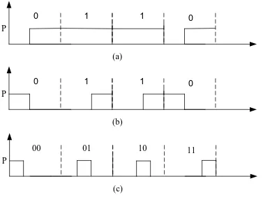
Fig 1: The waveforms of modulation techniques. (a) The signal waveform of VPPM transmission scheme (b) The signal waveform of VOOK transmission scheme (c) The signal waveform of traditional PPM transmission scheme.
Table 1. Codeword Table for Modulation Techniques
PCM PPM Offset PPM Shortened PPM
000 00000001 0000 00001
001 00000010 0001 00010
010 00000100 0010 00100
011 00001000 0100 01000
100 00010000 1000 10001
101 00100000 1001 10010
110 01000000 1010 10100
111 10000000 1100 11000
In Fig. 1.a, the VOOK signal is given for dimming factor δ=0.8. As shown in the figure, the all slots are filled when logical '1' data symbol is transmitted. For δ=0.8, there is 60% brightness in the other case that is data symbol being logical '0'. Additionally, data transmission cannot be achieved under full brightness and non-brightness [11].
In the VPPM scheme, logical '0' and logical '1' data bits are transmitted under equal brightness. However, the positions of signals are opposite the each other’s. This modulation technique is different from traditional PPM since its brightness is adjustable. In the traditional PPM scheme, one slot is filled the unlike VPPM. The position of filled slot is determined by using the decimal value of data bits. The
modulation technique can be considered as the shifting of filled slot from left side to right side.
methods compared with traditional PPM. The offset PPM technique was also proposed to shorten the SPPM signal
Comparator-2
(a=b)
Counter-1
Comparator-1
(a=b)
Sub
1
en
a
b
S.P
reset
Counter-2
Comparator-3
(a<b)
(c=b)
b
reset
M
u
x
1
n-1
n
SPPM
PCM
msb
a
[image:3.595.87.514.121.443.2]b
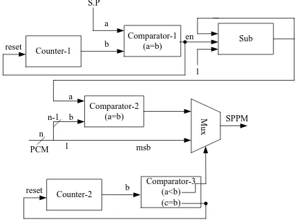
Fig 2: Proposed SPPM scheme
3.
THE PROPOSED SHORTENED PPM
TRANSMITTER ARCHITECTURE
In this section, we give the proposed shortened PPM scheme. The shortened PPM technique has appropriate transmission structure for shifting of data signal as shown in the Table I. The aim is to generate shortened PPM codeword that is separated from msb bit (Most Significant bit) in the first stage. Afterwards, the msb bit is added to encode shortened PPM bits.
In the Fig. 2, the proposed SPPM scheme is given for the design of digital circuit. In the first step, msb bit is excluded from data bits. As shown in the figure, the all data consists of n bits. The n-1 bits are applied to comparator-2 block while 1 bit, which is called as msb bit, is connected to input of mux. As shown in the table 1, the msb is logical '0' level for first half of PCM codewords while it is logical '1' level for other cases. This stage is referred as last step in this paper.
The decimal value of n-1 bits is compared to output of sub block. The sub block acts as an subtractor. It increases its output value for each slot period. The en signal, which is generated by comparator-1 block, is used to provide slot period intervals. The comparator-1 has two inputs which are slot period (S.P.) input and counter-1 output signal. The output of comparator (en signal) switches to logical '1' value when these signals are equal to each other’s. Otherwise, the
level of en signal is logical '0' level. The en signal is also used to reset counter-1 block, because the data rate is determined in this stage. In other words, this stage has some tasks follow as:
1- The assigning of data rate
2- The adjusting of slot period time
3- The generating of decimal value to determine position of logical '1' pulse.
Another stage is to determine position of logical '1' pulse. In this stage, comparator-2 and sub block serve as synchronize. The logical '1' signal is generated when the outputs of these blocks are equal to each other’s.
The msb bit of SPPM signal is determined in the last stage. In this stage, the selector signal is generated by comparator-3 block. The comparator-3 block has two outputs. The other output acts as a reset signal to control the counter-2 block. The stage decides which signal is activated among the msb and other bits. During the last slot time, the msb bit is selected in the output of mux block while n-1 bits are selected in other slot time.
4.
SIMULATION AND EXPERIMENTAL
RESULTS
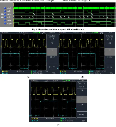
41 simulation results are taken from FPGA simulator program.
From experimental and simulation results, it is shown that the proposed architecture is practicable scheme since the output
[image:4.595.55.538.98.627.2]of oscilloscope and simulation results are similar. The SPPM signal is generated from one output pin for experimental results instead of the using ADC.
Fig 3: Simulation result for proposed SPPM architecture
(a) (b)
(c)
Fig 4: Experimental results for proposed SPPM architecture. For "abc" sequent PCM bits; (a) SPPM signal according to msb or a bit (b) SPPM signal according to b bit (c) SPPM signal according to c bit
In Fig. 3 and Fig. 4, we give simulation and experimental results for SPPM architecture. Fig. 3 presents simulation results. According to results, msb and data are defined as PCM bits. The data is decimal value of last two PCM bits. The sub result is obtained in the output of sub block. The aeb signal is output signal of comparator-2 block. In Fig. 4, the experimental results are given. If PCM bits are considered as "abc" sequent, the msb bit is a bit as shown in Fig. 4a. Fig 4b and Fig. 4c defines SPPM signal according to b and c bits.
5.
CONCLUSION
6.
REFERENCES
[1] M. Sui, X. Yu, Z. Zhou, “The modified PPM modulation for underwater wireless optical communication,” in Proc. ICCSN '09, 27-28 Feb. 2009, pp. 173-177.
[2] D. Anguita, D. Brizzolara, ve G. Parodi, “Optical wireless communication for underwater Wireless Sensor Networks: Hardware modules and circuits design and implementation”, OCEANS 2010 MTS/IEEE SEATTLE, 2010, pp. 1-8.
[3] D. Anguita, D. Brizzolara, ve G. Parodi, “VHDL modeling of PHY and MAC Layer modules for underwater optical wireless communication”, Proceedings of Papers 5th European Conference on Circuits and Systems for Communications (ECCSC’10), 2010, pp. 185-188.
[4] F. Akhoundi, J. A. Salehi, ve A. Tashakori, “Cellular Underwater Wireless Optical CDMA Network: Performance Analysis and Implementation Concepts”, IEEE Transactions on Communications, 63(3), pp. 882-891, Mar. 2015.
[5] I. Mizukoshi, N. Kazuhiko, ve M. Hanawa, “Underwater optical wireless transmission of 405nm, 968Mbit/s optical IM/DD-OFDM signals”, 2014 OptoElectronics
and Communication Conference and Australian Conference on Optical Fibre Technology, 2014, pp. 216-217.
[6] X. Shan, C. Yang, Y. Chen, ve Q. Xia, “A free-space underwater laser communication device with high pulse energy and small volume”, OCEANS 2017 - Anchorage, 2017, pp. 1-5.
[7] IEEE Standard 802.15.7-2011, pp. 1-309, Jun. 2011.
[8] J. Yoo, B. W. Kim, ve S. Jung, “Modelling and analysis ofM-ary variable pulse position modulation for visible light communications”, IET Optoelectronics, 9(5), pp. 184-190, 2015.
[9] M. Oh, “Pulse Dual Slope Modulation for VLC”, KSII Transactions on Internet and Information Systems, 8(4), pp. 1276-1291, Nis. 2014.
[10] Martin, J. N. S. (2011). “Analysis of offset pulse position modulation a novel reduced bandwidth coding scheme”. IET Optoelectronics, 5(4), p. 144-150.
[11] K. Lee ve H. Park, “Modulations for Visible Light Communications With Dimming Control”, IEEE Photonics Technology Letters, 23(16), ss. 1136-1138,