HIGH-STEP-UP INTERLEAVED DC
V. Anto Sahaya Varghese and S. Prathiba
Department of Electrical and Electronics Engineering,
ARTICLE INFO ABSTRACT
This paper presents a high a common active
interleaved. A boost converter is used to clamp the volt
interleaved converters, caused by the leakage inductances present in the practical coupled inductors, to a low voltage level. The leakage energies of the interleaved converters are collected in a clamp capacitor and
modulation concepts for multilevel
reduced chip size of the power semiconductors are proposed.
efficiency because of the recycling of the leakage energies, reduction of the switch voltage stress, mitigation of the output diode’s reverse recovery problem, and interleaving of the converters. A prototype of the proposed conver
validation.
INTRODUCTION
In many applications, high-efficiency, high
dc–dc converters are required as an interface between the available low voltage sources and the output loads, which are operated at much higher voltages. Examples of such applications are as follows. Different distributed energy storage components such as batteries, fuel cells, and ultracapacitors are used in the power trains of hybrid electric vehicles (HEV), electric vehicles (EV), and fuel cell vehicles (FCV). In the present power train architectures of these vehicles, the voltage levels of the energy storage elements are usually low, whereas the motors of the vehicles are driven at much higher voltages [1]–[4]. Next, the telecom and the computer industry utilize the standard batteries, with low voltage levels, as a back-up power source [5], [6]. In such applications, a front-end converter with dual inputs is used.The dc–dc converter, used in this case, is required to boost the low-input voltage of the batteries to the hig
of the dc bus. Another example is the automotive headlamps, using the high-intensity discharge lamp ballasts [5], [7].
The dc–dc converter, used in this application, is required to boost the low voltage level of car battery to much higher voltage level during the start-up and normal operations. Finally, few emerging applications, such as photovoltaic cells, also require high-gain dc voltage conversion [8]. It can be noted that in all these applications, the high
converters can be nonisolated but they should operate at high efficiency while taking high currents from low
sources at their inputs. In a conventional boost converter, the duty ratio increases as the output to input voltage ratio
*Corresponding author:[email protected]
ISSN: 0975-833X
Article History:
Received 27th April, 2012
Received in revised form 15th May, 2012
Accepted 12th June, 2012
Published online 30th July, 2012
Key words: Active-clamp, Boost converter,
Coupled-inductor boost converter, Dc–Dc power converter, High voltage gain, Interleaving.
RESEARCH ARTICLE
UP INTERLEAVED DC-DC CONVERTER WITH COUPLED
V. Anto Sahaya Varghese and S. Prathiba
Department of Electrical and Electronics Engineering, Easwari Engineering College, Chennai
ABSTRACT
This paper presents a high-efficiency and high-step-up nonisolated interleaved dc a common active-clamp circuit. In the proposed converter, the coupled
interleaved. A boost converter is used to clamp the voltage stresses of all the switches in the interleaved converters, caused by the leakage inductances present in the practical coupled inductors, to a low voltage level. The leakage energies of the interleaved converters are collected in a clamp capacitor and recycled to the output by the clamp boost converter. A
modulation concepts for multilevel dc–dc boost converter enabling a significantly less loss and a reduced chip size of the power semiconductors are proposed. The propose
efficiency because of the recycling of the leakage energies, reduction of the switch voltage stress, mitigation of the output diode’s reverse recovery problem, and interleaving of the converters. A prototype of the proposed converter is developed, and its experimental results are presented for validation.
Copy Right, IJCR, 2012, Academic Journals
efficiency, high-voltage step-up dc converters are required as an interface between the available low voltage sources and the output loads, which are operated at much higher voltages. Examples of such applications are as follows. Different distributed energy storage components such as batteries, fuel cells, and ultracapacitors are used in the power trains of hybrid electric vehicles (HEV), electric vehicles (EV), and fuel cell vehicles sent power train architectures of these vehicles, the voltage levels of the energy storage elements are usually low, whereas the motors of the vehicles are driven at [4]. Next, the telecom and the dard batteries, with low up power source [5], [6]. In such end converter with dual inputs is dc converter, used in this case, is required to input voltage of the batteries to the high voltage of the dc bus. Another example is the automotive headlamps,
intensity discharge lamp ballasts [5], [7].
dc converter, used in this application, is required to boost the low voltage level of car battery to much higher up and normal operations. Finally, few emerging applications, such as photovoltaic cells, gain dc voltage conversion [8]. It can be noted that in all these applications, the high-step-up dc–dc onisolated but they should operate at high efficiency while taking high currents from low-voltage dc
sources at their inputs. In a conventional boost converter, the duty ratio increases as the output to input voltage ratio
increases. However, the previously mentioned applications require high-voltage step-up and high
conversion. Therefore, the conventional boost converters will require extreme duty ratios to meet the high
requirements [9]–[12]. Under such conditions, it is a major challenge to operate the boost converters at high efficiency [15]. This is because, with the high
switch has to block a large voltage and hence the ON resistance, RDS-ON, which varies
the square of blocking voltage, will be very high. Furthermore, the low-level input voltages cause large input currents to flow through the switches. The extreme duty
short-pulsed currents with high amplitu
output diodes and the capacitors; which cause severe diode reverse recovery problem and increases in the conduction losses. The high RDS-ON of the switches, the increased conduction losses, and the severe reverse
will degrade the efficiency and limit the power level of the conventional boost converters [15]. Moreover, the parasitic ringing, present in the practical circuits, induces additional voltage stresses and necessitates the use of switches with higher blocking voltage ratings, which will lead to more losses. The coupled-inductor boost converter can be a good solution to the previously discussed problems of the conventional boost converter is shown in Fig. 1. This is because the turns ratio of the primary inducto
secondary inductor (L2) of the coupled inductor can be effectively used to reduce the duty ratio and the voltage stress of the switch [5], [10]. Therefore, for high
applications, the coupled-inductor boost converter can be more efficient than the conventional boost converter. However, for high power applications, handling of very large input currents from the low-input voltage sources remains a
International Journal of Current Research
Vol. 4, Issue, 07, pp.075-080, July,2012
INTERNATIONAL
DC CONVERTER WITH COUPLED-INDUCTOR
Easwari Engineering College, Chennai-89
up nonisolated interleaved dc–dc converter with clamp circuit. In the proposed converter, the coupled-inductor boost converters are age stresses of all the switches in the interleaved converters, caused by the leakage inductances present in the practical coupled inductors, to a low voltage level. The leakage energies of the interleaved converters are collected in a clamp recycled to the output by the clamp boost converter. A new topologies and interleaving boost converter enabling a significantly less loss and a The proposed converter achieves high efficiency because of the recycling of the leakage energies, reduction of the switch voltage stress, mitigation of the output diode’s reverse recovery problem, and interleaving of the converters. A ter is developed, and its experimental results are presented for
, Academic Journals. All rights reserved.
increases. However, the previously mentioned applications up and high-efficiency power conversion. Therefore, the conventional boost converters will require extreme duty ratios to meet the high-voltage step-up ]. Under such conditions, it is a major challenge to operate the boost converters at high efficiency [15]. This is because, with the high-output voltage, the boost switch has to block a large voltage and hence the ON-state ON, which varies almost proportionally with the square of blocking voltage, will be very high. Furthermore, level input voltages cause large input currents to flow through the switches. The extreme duty-cycle operation drives pulsed currents with high amplitude to flow through the output diodes and the capacitors; which cause severe diode reverse recovery problem and increases in the conduction ON of the switches, the increased conduction losses, and the severe reverse-recovery problem l degrade the efficiency and limit the power level of the conventional boost converters [15]. Moreover, the parasitic ringing, present in the practical circuits, induces additional voltage stresses and necessitates the use of switches with voltage ratings, which will lead to more inductor boost converter can be a good solution to the previously discussed problems of the conventional boost converter is shown in Fig. 1. This is because the turns ratio of the primary inductor (L1) to the 2) of the coupled inductor can be effectively used to reduce the duty ratio and the voltage stress of the switch [5], [10]. Therefore, for high-voltage step-up inductor boost converter can be e efficient than the conventional boost converter. However, for high power applications, handling of very large input voltage sources remains a
practical issue. Various converter topologies using magnetically coupled inductors are reported in the literature to reduce to the extreme duty ratio operation for nonisolated high step-up applications [8]–[14]. But they are not suitable for high current and high power applications, and moreover, the circuits are complex to design and model. For high-input current, it can be proposed to interleave the coupled-inductor boost converters to process high power, and to achieve high efficiency and high reliability with reduced size inductors and capacitors [17].
Fig. 1 Coupled-inductor boost converter
Various advantages of interleaving are well reported in the literature [10], [11], and [12]. The schematic diagram of the proposed interleaved coupled-inductor boost converter is shown in Fig. 3. An interleaved boost converter with three winding-based coupled inductors is reported in [11] and [12]. This converter has two interleaved cells, and the inductors of one interleaved cell are coupled with the inductors of the other interleaved cell. Therefore, with this converter the modular structure, which is a key beneficial feature of the interleaved converters, cannot be realized. Furthermore, the maximum number of interleaved cell is only two in this converter.
The interleaved converter, presented in this paper, is modular and can be designed for any number of cell. In a practical coupled inductor, there will be considerable amount of leakage inductance present due to the non-ideal coupling between the primary inductor (L1) and the secondary inductor (L2). The leakage inductance causes high voltage stresses to the switches, large switching losses, parasitic ringing, and severe electromagnetic interference problems, which degrade the converter performances [8] and [18]. Resistor–capacitor–diode (RCD) based snubber circuits can be used to mitigate the problem, but the losses in these circuits are very high [12] and [18]. Active-clamp circuits can be used to address this issue [12]. Moreover, the efficiency improvement in these circuits is limited by the high conduction loss in the active-clamp switches.
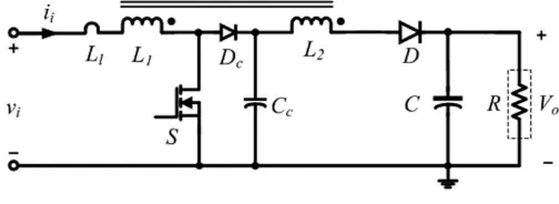
A diode and capacitor-based passive-clamp circuit is shown in Fig. 2. In this clamp circuit, the clamp capacitor (Cc) is discharged to the output through the secondary side inductor (L2) of the coupled-inductor boost converter. However, the clamp diode (Dc), in this circuit, is in series with the coupled inductor. Therefore, it’s not only the leakage inductance current, but the total coupled-inductor current, which flows through the clamp diode (Dc). This causes large losses in the clamp diode. The clamp diode needs to be rated for the entire large power processed by the coupled-inductor boost converter. This can make the converter operation inefficient for the higher power applications. Furthermore, in this clamp circuit, to take the advantages of the reduced switch voltage stress feature of the coupled-inductor boost converter, the clamp capacitor has to be considerably large, capable of
handling the high amount of charge, and discharge currents of the converter. Also, this will cause additional losses in the clamp capacitor. It can be noted that, if any of the previously discussed clamp circuit is used in the interleaved coupled-inductor boost converter; each of the interleaved phases of the converter will require additional clamp circuit components and control circuits (for active clamp). This will increase the cost, size, and complexity.
Fig. 2 Coupled-inductor boost converter with clamp circuit
A single active-clamp circuit can be proposed, in which the energy stored in leakage inductances of all the interleaved Coupled-inductor boost converters are gathered in a common clamp capacitor [9]. In each of the interleaved units, a clamp diode is connected from the common node of the coupled inductors to the clamp capacitor for providing the discharge path of the leakage energy. Therefore, only the leakage currents flow through the clamp diodes; this makes the clamping operation efficient. A simple boost converter is used to recycle the leakage energy, gathered in the clamp capacitor, to the output of the interleaved converter. The boost converter is controlled to keep the clamp-capacitor voltage to a low level, and hence, the voltage stress on the switches is low. This allows the use of low-voltage and high-performance devices. It can be noted that, a conventional boost converter can be used for the clamp circuit, because the ratio of the output voltage to the clamp voltage is not very high.
II. Interleaved coupled-inductor converter
In high current or high power application, interleaving of boost converters are well established. To take benefit of the advantages of interleaving, interleaved coupled-inductor boost converter can be used. In this approach, a single
coupled-inductor boost converter cell is treated as a cell and n such
cells are connected in parallel and operated at the same switching frequency. Furthermore, all the cells are operated at the same duty ratio. It can be mentioned that due to interleaving, the effective switching frequency as seen by the input and the output of the interleaved converter circuit is n times higher than the switching frequency of a phase. Under normal or full-load condition, each of the interleaved cells equally shares the total output load. But under lower output power demand condition, the number of operating cells can be adjusted for maximum efficiency operation of the individual
cells. The number of parallel cells n in an interleaved
[image:2.595.43.281.181.269.2]Fig. 3 Proposed interleaved coupled-inductor boost converter with single boost converter clamp
This results in a high-voltage stress across the switches and in ringing losses. It can be proposed to clamp the switch voltage to the output voltage, using a parallel diode. In this clamp circuit, the energy stored in the leakage inductance is discharged directly to the output by the parallel diode, and the switch voltage is clamped to the output voltage. It can be seen that this converter avoids the disadvantage of series conduction loss of the total power, but the switch voltage stress becomes equal to the output voltage. So this configuration does not take full advantages of the coupled-inductor boost topology, and hence, it is not suitable for high-step-up application where the output voltage level is high. The output voltage is given by,
Vo = Vs + L ΔI / t2 = Vs (1 + t1 / t2)
Peak to peak voltage is given by,
ΔVc = 1/C 0ʃt1 Io dt = Io t1 / C
ΔVc = Io (Vo - Vs) / Vo f C = Io K / f C
To lower the voltage stress on the switches close to the level of the voltage stress present in an ideal coupled-inductor boost converter, a common active-clamp circuit based on a boost converter can be proposed, as shown in Fig. 4. In the proposed
active-clamp circuit, in each cell, a clamp-diode (Dc1, Dc2, . .
. Dcn) is connected to the common node of the primary
inductor, the secondary inductor, and the switch of an interleaved coupled-inductor boost converter. The cathode terminals of all the clamp diodes are connected to a clamp capacitor Cc. The energies stored in the leakage inductors of the interleaved phases are discharged through the clamp diodes and gathered in the clamp capacitor Cc. Furthermore, the boost converter is used to transfer the stored energy in the clamp capacitor to the output of the interleaved converters, while maintaining the voltage level of the clamp capacitor to a lower level is shown in Fig. 3. The voltage stress on the
switches (S1, S2, . . . Sn) is decided by this clamp-capacitor
voltage. It can be suggested that any other converter topology, which can perform similar boost operation while maintaining the voltage level of the clamp capacitor can be also used for the active-clamp operation.
III. Clamp boost converter
From the previous analysis, it can be seen that the energy stored in all the leakage inductances of the interleaved coupled-inductor boost converters are discharged to the capacitor (Cc). To clamp the switch voltages of the interleaved converter, the voltage of the capacitor has to be controlled. In this paper, a simple boost converter is used for this purpose. The boost converter transfers the leakage energy stored in this clamp capacitor (Cc) to the output and maintains its voltage to a desired clamp voltage level. So, the power rating of the clamp boost converter is decided by the maximum total leakage energy of the interleaved converters. It can be noted that unlike the regular boost converters, which have a fixed input voltage and a variable output voltage, this clamp boost converter has a fixed output voltage but a variable input voltage. This is because the total leakage energy of the interleaved converters is very small compared to the total output power of the interleaved converters. Therefore, the voltage at the output of the clamp boost converter is decided by the interleaved coupled-inductor boost converters.
The inductor and capacitor is given by,
L = K (1-K) R / f = Vs K / f I
C= K / f R = K I / V f
The duty ratio of the clamp boost converter can be controlled to discharge the leakage energy stored in the clamp capacitor (Cc) to the output dc bus and maintain its input voltage to a reference clamp voltage level. The clamp voltage level decides the voltage stresses on the switches of the coupled-inductor boost converters. With low switch voltage stress, the converter can be designed to deliver power at high efficiency even when considerable amount of leakage inductance is present in the couple inductors. The clamp boost converter can be operated either in continuous conduction mode (CCM) or in discontinuous conduction mode (DCM). Under CCM, the switching losses are more than the switching losses under DCM. However, the conduction losses under the DCM are more than the conduction losses under the CCM. The clamp boost converter, considered in this study, processes small amount of power obtained from the leakage inductances of the interleaved converters and the voltage level at the clamp capacitor (Vcmin) is quite higher than input voltage level (Vi). Therefore, the average inductor current of the clamp boost converter is small. But the MOSFET of the clamp boost converter switches at high voltage levels. Therefore, in this paper, the clamp boost converter is chosen to operate in DCM
to reduce the losses in the clamp boost converter.
IV. Modes of operation
boost converter. The operation modes for one of the interleaved cell are shown in Fig. 4, 5, 6. The non-ideal coupled inductors of the interleaved phases can be modeled by a magnetizing inductor (Lm1), which is connected in parallel with an ideal transformer and a series leakage inductor (Ll1). The turns ratio of the transformer is equal to the primary to the secondary turns ratio (1:N) of the coupled inductor. The value of the magnetizing inductance can be obtained by subtracting the leakage inductance value from the primary winding inductance value of the coupled inductor. The input current and the output current of the interleaved phase are defined in this equivalent model. These operation modes are discussed as follow.
Stages of Operation
Stage 1 (t ∈[t0, t1 ])
Fig. 4 Stage 1 Operation
This stage begins when the switch S1 is turned on. The output
diode D1 is reverse biased, and the input voltage Vicharges
the primary inductor (Lm1) and the leakage inductor (Ll1). The input current and the output current of the interleaved phase are defined in this equivalent model. The leakage energies are discharged by the clamping diodes and collected in the capacitor Cc. The clamping voltage will appear across the output voltage
Stage 2 (t ∈[t1, t2 ])
This stage starts when the switch S1 is turned off. The leakage inductor (Ll1) forward biases the clamp diode Dc1 and the energy stored in the leakage inductor is discharged to the clamp capacitor Cc. This causes a discharge current spike. The peak of this current is equal to the maximum value of the input current reached at the end of stage-1. At the same instant, when the switch S1 is turned off, the stored energy in the magnetizing inductor (Lm1) forward biases diode D1 at the secondary side of the coupled inductor.
The voltage difference between the converter output and the input (Vo − Vi) is divided as per the turns ratio of the ideal transformer and the voltage at the point A. It can be noted that the fall rate of the leakage current is decided by the voltage
difference between the clamp capacitor voltage and the
voltage at the node A. The slope of the input and the output current of the converter during stage-2 are defined by the slopes of the magnetizing current and the leakage inductor current.
Fig. 5 Stage 2 Operation
Stage 3 (t ∈[t2, t3 ])
Fig. 6 Stage 3 Operation
This stage begins when the leakage inductor current value has become zero, and the leakage energy is completely discharged. The clamp diode Dc1 is reversed biased by the clamp voltage Vc. The output diode D1 remains forward biased and the voltage at the point A. The energy to the output is transferred from the magnetizing inductor and from the
source. The switch S1 remains turned off. The leakage
energies are discharged by the clamping diodes and collected in the capacitor Cc. The clamping voltage will appear across the output voltage.
V. Simulation Results
recovered leakage energy, and the other benefits of an ideal coupled-inductor boost converter and interleaving, the converter can achieve high efficiency for high-step-up power conversion.
[image:5.595.307.558.51.265.2][image:5.595.39.284.102.319.2]
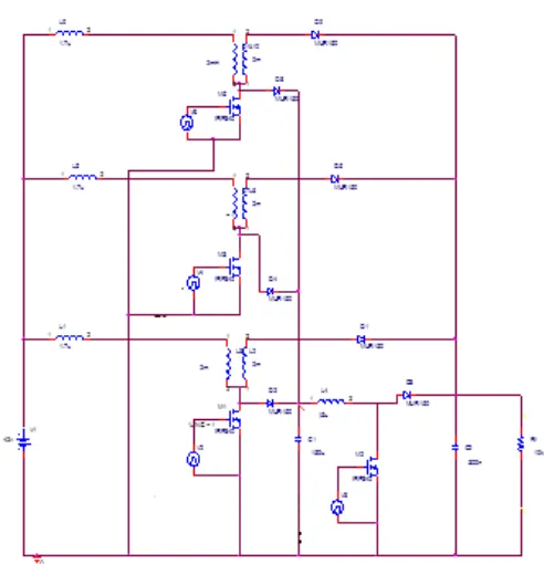
Fig. 7. Interleaved Coupled Inductor Boost Converter
Fig. 8. Output Voltage
VI. EXPERIMENTAL RESULTS
In high current or high power application, interleaving of boost converters are well established. To take benefit of the advantages of interleaving, interleaved coupled-inductor boost converter with a common active clamp circuit can be used. In this clamp circuit, the energy stored in the leakage inductance is discharged directly to the output by the parallel diode, and the switch voltage is clamped to the output voltage. The block diagram of hardware is shown in Fig. 9. A prototype of interleaved coupled-inductor boost converter with a common clamp boost converter is developed and tested. The prototype is shown in Fig. 11.
[image:5.595.305.558.293.466.2]Fig. 9. Block Diagram
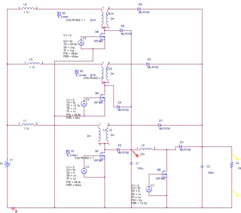
[image:5.595.42.290.358.495.2]Fig. 10. Proposed Interleaved Boost Converter
Fig. 11. Prototype of Interleaved Coupled Inductor Boost Converter
Fig. 12 Voltage Waveform
VII. Conclusion
Coupled-inductor boost converters can be interleaved to achieve high-step-up power conversion without extreme duty ratio operation while efficiently handling the high-input current. In a practical coupled-inductor boost converter, the switch is subjected to high voltage stress due to the leakage D4 MUR150 V1 42v C1 150u V+ 0 D5 MUR150 L5 1.7u 1 2 KK2
COUPLING = 1
K_Linear M3 IRF840 L6 2m 1 2 D8 MUR150 L4 15u 1 2 L7 2mH 1 2 KK1
COUPLING = 1
K_Linear L9
1.7u
1 2
V3
TD = 0 TF = 1n PW = 2u PER = 13.3u V1 = 0 TR = 1n V2 = 5v
L2 2m 1 2 R1 10k M2 IRF840 D9 MUR150 L1 1.7u 1 2 L3 2m 1 2 L10 2m 1 2 V2
TD = 0 TF = 1n PW = 26.6u PER = 40us V1 = 0 TR = 1n V2 = 5v
L11 2mH 1 2 M1 IRF840 D1 MUR150 V6
TD = 26.6u TF = 1ns PW = 26.6u PER = 40us V1 = 0
TR = 1ns V2 = 5v
M5
IRF840
KK3
COUPLING = 1
K_Linear
V4
TD = 13.3u TF = 1n PW = 26.6u PER = 40u V1 = 0 TR = 1n V2 = 5v
V D2 MUR150 C2 300n V-D3 MUR150 L4 15u 1 2 LED 1 2 M2 IRF840 R1 10k M3 IRF840 74LS125A 7 L3 2m 1 2 M1 IRF840 TLP250 R7 1k V1 42v A1 2 D2 1N4500 12 M5 IRF840 D4 1N4500 1 2 PIC12F508 4 C2 R1 D3 1N4500 1 2 R6 1k A4 D1 1N4500 12 8 D2 1N4500 12 LED1 2 7812 1 3 2 INOUT GND L5 1.7u 1 2 1 TX1 2 3 0-1 5V -5 00 m A D4 1N4500 1 2 D4 1N4500 1 2 R2 1k Y2 9 A2 D2 1N4500 12 C2 10u C3 C1 1 0 00 u D3 1N4500 1 2 L7 2mH 1 2 11 D5 MUR150 D4 1N4500 1 2 C2 300n GP5/OSC1/CLKIN 7812 1 3 2
INOUTGN
D
KK3
COUPLING = 1
K_Linear R9 1k 12 C1 150u D4 MUR150 C2 10u C1 TX1 2 3 0-15 V -50 0 m A VDD D3 1N4500 1 2 Y1 14 C1 1 00 0 u KK1
COUPLING = 1
K_Linear D1 1N4500 12 C4 Y4 0 C2 10u L2 2m 1 2 GND D2 MUR150 R1 GP3/MCLR/VPP 7805 1 3 2
INOUTGN
D D1 1N4500 12 D3 1N4500 1 2 D1 MUR150 TX1 23 0 -1 5 V -5 0 0m A D1 1N4500 12 KK2
COUPLING = 1
[image:5.595.306.555.509.667.2] [image:5.595.39.289.663.773.2]inductance present in the non-ideal coupled inductor. The presented active-clamp circuit, based on single boost converter, can successfully reduce the voltage stress of the switches close to the low-level voltage stress offered by an ideal coupled-inductor boost converter. The common clamp capacitor of this active-clamp circuit collects the leakage energies from all the coupled-inductor boost converters, and the boost converter recycles the leakage energies to the output. Detailed analysis of the operation and the performance of the proposed converter were presented in this paper. It has been found that with the switches of lower voltage rating, the recovered leakage energy, and the other benefits of an ideal coupled-inductor boost converter and interleaving, the converter can achieve high efficiency for high-step-up power conversion. A prototype of interleaved coupled-inductor boost converter with a common active clamp circuit was implemented and the results are obtained.
REFERENCES
[1] Q. Zhao and F. C. Lee, “High-efficiency, high step-up
DC–DC converters,” IEEE Trans. Power Electron., vol. 18, no. 1, pp. 65–73, Jan.2003.
[2] S. Dwari and L. Parsa, “A novel high efficiency high
power interleaved coupled-inductor boost DC-DC converter for hybrid and fuel cell electric vehicle,” in Proc. IEEE Veh. Power Propulsion Conf. 2007, pp. 399–404.
[3] W. Li and X. He, “An interleaved winding-coupled
boost converter with passive lossless clamp circuits,” IEEE Trans. Power Electron., vol. 22, no. 4, pp. 1499– 1507, Jul. 2007.
[4] G. C.-Lopez, A. J. Forsyth, and D. R. Nuttall, “Design
and performance evaluation of a 10-kW interleaved boost converter for a fuel cell electric vehicle,” in Proc. IEEE Power Electron. Motion Control Conf.,Aug. 2006, vol. 2, pp. 1–5.
[5] J.Marshall andM. Kazerani, “Design of an efficient fuel
cell vehicle drive train, featuring a novel boost converter,” in Proc. IEEE Ind. Electron. Soc Annu. Conf., Nov. 2004, pp. 1229–1234.
[6] W. Rong-Jong and D. Rou-Yong, “High step-up
converter with coupled-inductor,” IEEE Trans. Power Electron., vol. 20, no. 5, pp. 1025–1035, Sep. 2005.
[7] J. Bauman and M. Kazerani, “A comparative study of
fuel battery, fuel ultracapacitor, and fuel cell-battery-ultracapacitor vehicles,” IEEE Trans. Veh. Technol., vol. 57, no. 2, pp. 760–769, Mar. 2008.
[8] I. Barbi and R. Gules, “Isolated DC-DC converters with
high- output voltage for TWTA telecommunication satellite applications,” IEEE Trans.Power Electron., vol. 18, no. 4, pp. 975–984, 2003.
[9] E. J. Cegnar, H. L. Hess, and B. K. Johnson, “A purely
ultracapacitor energy storage system hybrid electric vehicles utilizing a based DC-DC boost converter,” in Proc. Appl. Power Electron. Conf. Expo., IEEE, 2004, vol. 2, pp. 1160–1164.
[10] N. Mohan, T. M. Undeland, and W. P. Robbins, Power
Electronics, 3rd ed. New York: Wiley, 2002.
[11] C. Chang and M. A. Knights, “Interleaving technique in
distributed power conversion systems,” IEEE Trans. Circuits Syst. I: Fund. Theory Appl., vol. 42, no. 5, pp. 245–250, May 1995.
[12] M. T. Zhang, M. M. Jovanovi´c, and F. C. Lee,
“Analysis and evaluation of interleaving techniques in forward converters,” IEEE Trans. Power Electron., vol. 13, no. 4, pp. 690–698, Jul. 1998.
[13] Jungwan Choi, Hanju Cha and Byung-Moon Han, “A
three phase interleaved DC-DC converter with active clamp for fuel cells,” IEEE Trans. Power Electron., vol. 25, no. 8, pp. 2115–2123, Aug. 2010.
[14] S. K. Changchien, T. J. Liang, J. F. Chen and L. S.
Yang, “Novel high-step-up DC-DC converter for fuel cell energy conversion system,” IEEE Trans. Ind. Electron., vol. 57, no. 6, pp. 2007–2017, Jun. 2010.
[15] Wuhua Li, Yi Zhao, Yan Deng, X. He, “Interleaved
converter with voltage multiplier cell for high step-up and high-efficiency conversion,” IEEE Trans. Power Electron., vol. 25, no. 9, pp. 2397–2408, Sep. 2010.
[16] Shin H. B, “Small-signal analysis of multiphase
interleaved boost converter with coupled inductors,” IEEE Trans. Power Electron., vol. 152, no. 5, pp. 1161– 1170, Sep. 2005.
[17] Po-Wa Lee, Yim-Shu Lee, Cheng D. K. W, Xiu-Cheng
Liu, ”Steady-state analysis of an interleaved boost converter with coupled inductors,” IEEE Trans. Ind. Electron., vol. 47, no. 4, pp. 787–795, Aug. 2000.
[18] Y. Zhao, W. Li, Y. Deng, X. He, “High step-up boost
converter with passive lossless clamp circuit for non-isolated high step-up applications,” IEEE Trans. Power Electron., vol. 4, no. 8, pp. 851–859, Sep. 2011.