Abstract—As different tool materials are hard to machine by routine micromachining techniques, Focused Ion Beam (FIB) technique is used for fabrication of microtools. This paper aims to comprise a detailed review on microtools fabrication by FIB and a step by step procedure of fabricating microtools is explained. Operating parameters are briefly described to show their significance for microtools fabrication. The operating parameters of FIB machining presented here do not only give information about material removal rate but also helpful for achieving desired surface finish of microtools. In addition, new geometry of micro end mill cutter is also proposed.
Index Terms— Focused Ion Beam (FIB) Milling, FIB system, Microtools Fabrication.
I. INTRODUCTION
Focused ion beam (FIB) technology is an extremely important tool in semiconductor device manufacturing. It is an invaluable tool for failure analysis and design work [1], as well as lithographic mask repair [2], cross sectioning of devices [3], maskless implantation [4], [5] and ion beam assisted etching [6], [7]. FIB machining finds increasing applications for producing precisely located micro scale integrated circuit features. Recent FIB systems provide a unique capability for the microscopic examination of IC artifacts for failure analysis, by the addition of scanning electron microscope (SEM) facility [8]. In addition to the removal of material through micro machining, techniques have been established for the precise deposition of material in patterns. Recently FIB technology is applied to produce objects with feature sizes at micro/nano scale.
Several IC manufacturing techniques apply only on silicon. However, miniaturization needs to be applied on all materials. A suitable machining technique is needed to manufacture micro/nano features on all materials. FIB machining satisfies such requirement. It addresses the issues related to machining of polymers, insulators, semiconductors and metals. Apart from the applications of FIB technology in semiconductor industries, it has found its profound utility in the field of mechanical engineering too. Fabrication of microtools for microlathe machine and micromilling
Manuscript received on March 23, 2009.
Sanket N. Bhavsar is with Mechanical Engineering Department, Indian Institute of Technology Delhi, New Delhi – 110016, INDIA (e-mail: [email protected]).
Dr. S. Aravindan is with Mechanical Engineering Department, Indian Institute of Technology Delhi, New Delhi – 110016, INDIA (Corresponding Author, Phone: +91 11-26596350, e-mail: [email protected]).
Prof. P. Venkateswara Rao is with Mechanical Engineering Department, Indian Institute of Technology Delhi, New Delhi – 110016, INDIA (e-mail: [email protected]).
machines is the most important one. Moreover, atomic sized probes are also easily manufactured by FIB annular milling technique [9]-[11]. In short the area of applications and the materials on which the FIB technology is applicable is really endless [12]-[14]. This paper is the review of microtools fabrication using FIB technology. Here, the manufacturing procedure of microtools has been explained with FIB operating parameters. Moreover, the different alternatives of microtools fabrication using FIB technique have been analyzed for required cutting edge radius and surface finish of tool face.
A. Basic Principle of FIB Technology
In FIB technology, ion beam with specific intensity and diameter is directed to substrate material for micro/nano fabrication process. When an energetic ion hits the target surface, various ion-target interactions like swelling, deposition, milling, implantation, backscattering, nucleation, etc can occur [15]. However, some of the interactions are not completely separable and may lead to unwanted side effects that need to be understood and avoided for a specific application. The most important interaction for milling is that the energy transferred from the ions to the target substrate is high enough, leading to a collision cascade involving substrate atoms at or near surface where sputtering or redeposition are the two governing effects that cause removal of material [16]-[18]. The sputtering yield, defined as the number of atoms ejected per incident ion, is a measure of the efficiency of material removal. The yield is normally in the range of 1-50 atoms per ion and is a function of many variables, including masses of ions and target atoms, ion energy, direction of incidence to the surface of the target, target temperature and ion flux. For material removal by collision cascade, the optimized energy is in the range of 10-100 keV.
B. FIB System
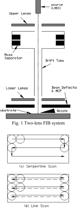
The basic components of a FIB system are normally an ion source, an ion optics column, a beam deflector and a substrate stage [19]. Fig. 1 schematically shows a FIB system with a two-lens (or twin-lens) column. The Liquid Metal Ion Source (LMIS) has been widely used to provide reliable and steady ion beams for a variety of ion species [20], [21]. Generally Ga+ ions are used as LMIS. The application of the critical Taylor voltage on the liquid metal cone extracts positively charged ions, which makes the beam.
The FWHM (full width at half maximum) is commonly used to describe the diameter of a FIB, in which the ion intensity is highly non-uniformly distributed; frequently, its intensity is close to a Gaussian profile. The FWHM is defined as the distance between the locations on the intensity profile
A Critical Review on Microtools Fabrication by
Focused Ion Beam (FIB) Technology
at which the intensity reaches half of its maximum value [22].
II. FIB MILLING
[image:2.595.92.256.169.613.2]For FIB milling, the Ga+ ion beam can either digitally raster scanned in a serpentine pattern over the rectangular region to be milled or line scanned over a line which can then systematically stepped to form a rectangular region as shown in Fig. 2.
Fig. 1 Two-lens FIB system
Fig. 2 Scanning of a rectangular pattern
Material removal by FIB machining relies upon the process of sputtering to erode target surfaces and as a ‘cold’ process FIB machining has advantages over methods which heat substrates causing unwanted thermal damage, even melting. The depth etch rate for a sputter yield of Y surface atoms per incoming ion, using a probe of current I is given by (1),
⎟
⎠
⎞
⎜
⎝
⎛
=
e
I
A
YM
dt
dz
ρ
(1) where A is the etched area, ρ is the density of targetmaterial, M is atomic mass of target material and e the
electronic charge [23].
A software package, TRIM (TRansport of Ions in Matter), has been widely used for predicting the sputtering yield for many different ions at a wide range of energy. TRIM is a comprehensive Monte Carlo program, which calculates the stopping range of ions (10 eV–2GeV per atomicmass unit) into matters using a quantum mechanical treatment of ion–atom collisions [24].
III. MICROTOOLS FABRICATIONS
A. Microtools for Microlathe Machine
Development of cutting tools with micro/nano level features is a difficult task. The diamond indenters having facets at micron level features can be either machined by laser or ion beam machining. The resolution of ion beam and laser beam puts a restriction for the production of micro tools with nano level features. Diamond cutting tools having nano level tool geometrical features can only be produced through focused ion beam machining.
Lu Z and Yoneyama [25] describe a micro machining system and emphasize the need for miniaturization of cutting tools in order to achieve the potential of the micro lathe. The Micro cutting tools with dimensions in the range of 15-100
μm can be easily manufactured by FIB sputtering. Complex geometric features like tool nose radius, rake angles and relief angles are controlled in nm range. Variety of tool geometries were produced with the help of FIB sputtering technique on the tool materials such as tungsten carbide, high-speed tool steel and single crystal diamond [26].
Comparing with high-speed steel and tungsten carbide tool material, diamond requires significantly longer machining time due to higher C-C surface bonding energy. With regard to FIB fabrication process the steel and carbide require smaller time for shaping. A 25 μm wide threading tool made up of steel or carbide can be fabricated in 3-5 hrs using a 2 nA ion beam. Use of commercial 20 nA ion source would reduce the fabrication time to less than 30 min for most tool geometry [26]. All tool materials were machined to have approximately 0.05 μm cutting edge roughness and 0.04-0.09
explained by researchers in Fig. 3 needs one more fifth step of material removal from side, like step two, to make the cutting edge, which has remained rounded at the end of step four, sharper at the end of all operations.
Fig. 3 Procedure for ion milling a micro-threading tool [26]
Fig. 4(a) shows low magnification perspective view of single crystal diamond tool connected to carbide shank. The cutting edges are fabricated near approximately 30 μm from the tool tip. Fig. 4(b) shows the high magnification scanning electron micrograph of the same diamond tool in perspective view to show the fabricated cutting edge and other facets. These kind of microtools are used for manufacturing micro solenoids (micro windings), Cu and Al mirrors used in CO2 laser and other micro machining applications.
Fig. 4 (a) Low magnification view of single
crystal diamond tool [26]
Fig. 4 (b) high magnification scanning
electron micrograph of same diamond tool [26] B. Microtools for Micromilling Machine
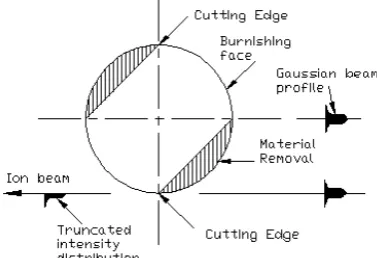
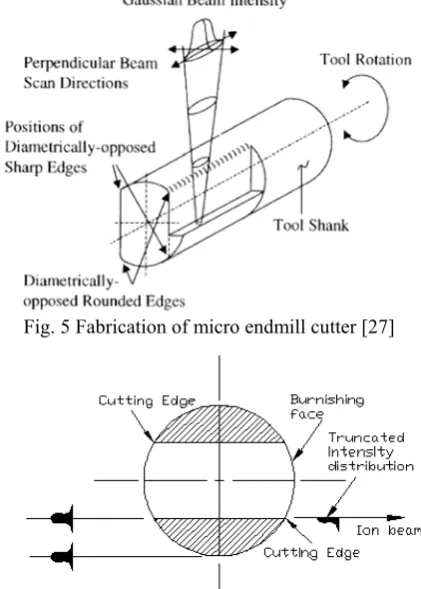
Micro end mill cutters are made with nonplanar facets by ion sputtering process as shown in Fig. 5 [27]. The end of the tool is bombarded to create a facet with a normal direction oriented 70 with respect to tool axis. This inclination of facet is intended to provide a clearance angle during machining. The sputtered facet edge closest to the ion source is rounded having a radius of curvature on the order of 1.0 μm. This rounding is due to the part of Gaussian beam intensity that extends outside the user defined pattern boundary. However, continued ion sputtering makes a sharp edge on the order of 0.1 μm on the other side of facet furthest from ion source. Because of truncated ion beam intensity distribution due to shadowing of the tool facet, a sharp edge is produced, which is a cutting edge. As the incidence angle of the ion beam with tool facet changes from 450 to normal, the sputtering yield and in turn efficiency of cutting facet varies. Fig. 6 shows the fabrication of two fluted endmill cutter. If four fluted tool is
[image:3.595.327.538.82.377.2]required, tool should be rotated 900 four times [28].
Fig. 5 Fabrication of micro endmill cutter [27]
Fig. 6 Schematics of cutting edge formation C. Cost Saving in Micromilling Tool Manufacturing
Wire Electro Discharge Grinding (WEDG) was considered as a cost saving alternative for microfabrication [29]. Fabrication of micromilling tools using WEDG and FIB sputtering has been analyzed and effect of FIB process parameters studied by researchers. For that tool blank of tungsten carbide was fabricated by WEDG and cutting edges were formed by FIB sputtering. Fig. 7 shows basic steps for the tool blank preparation using WEDG technique adopted by Ali and Ong [30]. Initially, the end of the rod was faced in order to ensure the flatness of the cutting tool tip. Then the diameter of the rod was reduced to 20 μm from 300 μm by moving it downwards (z-direction) with rotational speed of 3000 rpm. The diameter of the workpiece was determined by the wire position in x-direction. The workpiece moved down along z-direction with controlled speed and after required length of machining retracted back.
[image:3.595.61.288.96.250.2] [image:3.595.53.291.403.547.2]Fig. 7 Schematic diagram for the preparation of tool blank using WEDG technique [30]
Fig. 8 Cutting edges of the micromilling tool [30]
Fig. 9 Schematic diagram of FIB step-sputtering to form the cutting edges of the micromilling tool [30]
IV. OPERATING PARAMETERS OF FIB SYSTEM
The quantity of ions delivered to the substrate per unit area is known as ion doze. It is a function of beam current, dwell point spacing and dwell time. Ion doze can be translated into depth of sputtering for a given substrate material. The pixel doze, the number of ions per unit area, is determined by the Ga+ beam current, dwell time and pixel size. The total Ga+ doze is determined by the Ga+ beam current, the area of the machined region and machining time. The process of tracing closely spaced parallel lines for sputtering is called scanning. Each line is composed of an array of points, which are known as pixels and distance between adjacent pixel points is called pixel spacing. During scanning ion beam remains directed at a pixel point for a period of time, which is called dwell time. The time required to reposition the beam from the end of one scan line to the start of next scan line is called retrace time. If
the beam completes scanning of one full area, it is known as one raster. After completing one raster beam starts scanning again until the assigned doze is completed.
The angle between ion beam and surface normal is known as incidence angle and it has a dominant effect on material removal rate. Increasing the incidence angle increases the sputtering yield until it reaches its maximum near 800; then it decreases very rapidly to zero as the incident angle approaches 900. Actually, the amount of sputtering is dominated by surface collision cascades. Roughly speaking, as the angle of collision between the ions and target atoms increases from normal incidence, the possibility of the target atoms escaping from the surface during the collision cascades increases and eventually this leads to an increased sputter yield. After reaching a maximum, the sputter yield decreases again as the ion approaches glancing incidence because of the increase in reflected ions and the fact that more and more collision cascades terminate at the surface before they are fully developed [31], [32]. The incidence angle at which maximum material removal rate occur, varies from material to material.
Experiments have been conducted to evaluate the effect of dwell time on substrate material keeping the total raster time constant [33]. As the dwell time increases the total number of raster decreases and shorter dwell time has shorter raster time. The short raster time is compensated by increasing the total number of raster per operation keeping the total raster time constant. It is concluded through experiments that shorter dwell time produces more accurately defined geometry than longer dwell time for the same amount of total ion doze. Shorter dwell time also reduces surface and subsurface damages. Poor geometries are formed with heavy ion doze and longer dwell time because of redeposition of sputtered material. In case of shorter dwell time, each scan removes redeposited material from the previous scan to produce a superior quality of work geometry [34]. Shorter dwell time in the range of 1-10 μs was found appropriate by experimental work [30].
At a selected dose and accelerating voltage, small pixel spacing and large dwell time leads to deep sputtering depth. Similarly, high accelerating voltage, large aperture diameter, short pixel spacing and long dwell time are required to achieve higher MRR [35]. Investigation also includes prediction of sputtering depth and material removal rate (MRR) for given accelerating voltage, ion dose and pixel spacing.
V. DISCUSSION
surface is different. This method requires calculation of dwell time at each position on substrate for material removal rate. The hatched portion shown in Fig. 10 is required to be removed by FIB milling to produce straight fluted micro endmill cutter with two cutting edges.
Fig. 10 Fabrication of two fluted micro endmill cutter Fig. 11 again shows fabrication of micro endmill cutter with two cutting edges. Fig. 11(a) shows milling of first cutting edge. For milling of second cutting edge specimen is required to be rotated by 1800, which is shown in Fig. 11(b). Fig. 11(b) shows proposed geometry of micro endmill cutter with two cutting edges. Compared to the cutter geometry shown in Fig. 6, cutter with geometry shown in Fig. 11(b) is stronger. It is clearly indicated from Fig. 11(b) that material removal is half of the cutter shown Fig. 6. Hence, from strength point of view, cutter shown in Fig. 11(b) is stronger than the similar two fluted cutter shown in Fig. 6. Fig. 12 shows proposed geometry of four fluted micro endmill cutter, where it requires rotation of 900 after milling of each cutting edge by FIB. Similarly, other geometry and different number of cutting edges can be fabricated using FIB milling. It seems easier to control tool geometry like rake angle and clearance angle for the proposed geometry of micro endmill cutters shown in Fig. 11 and Fig. 12. One important factor that is always neglected is the resharpening of micro cutters by FIB milling. The proposed geometry of micro endmill cutter seems more compatible from cutting edge resharpening point of view.
Operating parameters discussed in the previous section can be correlated with the microtools fabrication technique. Relationship between ion dose and milling depth can be established for various tool materials keeping other operating parameters constant. In turn parameter optimization can be done for maximizing material removal to achieve the desired surface finish on tool face. One critical aspect in microtools fabrication by FIB technique is cutting edge radius and nose radius. Setting of proper operating parameters generates sharp cutting edge and sharp nose radius. Sharpness of cutting edge radius and nose radius also depends upon the ion beam position relative to tool blank. In addition to above mentioned scope of work, attention is also required to produce specific shape of flutes in case of micro endmill cutters. Three dimensional shapes of flutes are possible to be fabricated. Researchers have done work to produce three dimensional contours [36], [37], which can be extended to fabricate flutes with three dimensional shapes on micro endmill cutters.
(a) Milling of first cutting edge
[image:5.595.327.534.52.377.2](b) Miliing of second cutting edge after 1800 tool rotation Fig. 11 Alternative of fabrication of two fluted micro
endmill cutter
Fig. 12 Fabrication of four fluted micro endmill cutter
VI. CONCLUSION
[image:5.595.83.272.121.250.2] [image:5.595.327.536.407.569.2]REFERENCES
[1] T. B. Mark, and H. M. George, “Review article – Mass analysed secondary ion microscopy”, Review of Scientific Instruments, vol. 58(10), 1987, pp.1789 – 1805.
[2] P. D. Prewett, and P. J. Heard, “Repair of opaque defects in photomasks using focused ion beams”, J. Phys. D: Appl. Phys., vol. 20, 1987, pp.1207-1209.
[3] E. C. G. Kirk, R. A. McMahon, J. R. A. Cleaver, and H. Ahmed, “Scanning ion microscopy and microsectioning of electron beam recrystallized silicon on insulator devices”, J. Vac. Sci. Technol. B, vol.6(6), 1988, pp.1940-1943.
[4] C. Musil, J. Melngailis, S. Etchin, and T. Hayes, “Does rate effects in GaAs investigated by discrete pulsed implantation using a focused ion beam”, J Appl. Phys., vol. 80, 1996, pp.3727.
[5] C. Crell, S. Friedrich, H. U. Schreiber, and A. D. Weick, “Focused ion-beam implanted lateral field-effect transistors on bulk silicon”, J Appl. Phys., vol. 82, 1997, pp.4616.
[6] Y. Ochiai, K. Gamo, and S. Namba, “Pressure and irradiation angle dependence of maskless ion beam assisted etching of GaAs and Si”, J. Vac. Sci. Technol. B, vol. 3(1), 1985, pp.67-70.
[7] K. Ochiai, “Characteristics of maskless ion beam assisted etching of silicon using focused ion beams”, J. Vac. Sci. Technol. B, vol. 4(1), 1986, pp. 333-336.
[8] F. C. Van Den Heuvel, “Focused – ion – beam – induced tungsten deposition for IC repair”, Microelectronic Engineering, vol. 21, 1993, pp.209 – 212.
[9] T. F. Kelly, T. T. Gribb, J. D. Olson, R. L. Martens, J. D. Shepard, S. A. Wiener, T. C. Kunicki, R. M. Ulfig, D. R. Lenz, E. M. Strennen, E. Oltman, J. H. Bunton, and D. R. Strait, “First data from a commercial local electrode atom probe (LEAP)”, Microscopy and Microanalysis, vol. 10, 2004, pp. 373-383.
[10] D. J. Larson, A. K. Petford-Long, Y. Q. Ma, and A. Cerezo, “Information storage materials: nanoscale characterisation by three-dimensional atom probe analysis”, Acta Materialia, vol. 52, 2004, pp.2847.
[11] M. K. Miller, K. F. Russell, and G. B. Thompson, “Strategies for fabricating atom probe specimens with a dual beam FIB”, Ultramicroscopy, vol. 102, 2005, pp.287-298.
[12] H. Hosokawa, K. Shimojima, Chino, Y. Yamada, C. E. Wen, and M. Mabuchi, “Fabrication of nanoscale Ti honeycombs by focused ion beam”, Materials Science and Engineering A, vol. 334, 2003, pp.365-367.
[13] D. M. Thaus, T. J. Stark, D. P. Griffis, and P. E. Russell, “Development of focused ion-beam machining techniques for perm alloy structures”, J Vac Sci Technol B, vol. 14(6), 1996, pp.3928-3932.
[14] Tao Dai, Xiangning Kang, Bei Zhang, Jun Xu, Kui Bao, Chang Xiong, and Zizhao Gan, “Study and formation of 2D microstructures of sapphire by focused ion beam milling”, Microelectronic Engineering, vol. 85(3), 2008, pp.640-645.
[15] R. Steve, and P. Robert, “A review of focused ion beam applications in microsystem technology”, Journal of micromechanics and Microengineering, vol. 11, 2001, pp.287 – 300.
[16] P. D. Prewett, “Focused ion beam systems for materials anslysis and modification”, Vacuum, vol. 34, 931-939.
[17] A. A. Tseng, “Topical Review: Recent developments in micromilling using focused ion beam technology”, J. micromechanics and microengineering, vol.14, 2004, pp.15-34.
[18] K. Gamo, “Focused Ion Beam Technology”, Semicond. Sci. Technol., vol. 8 , 1993, pp.1118-1123.
[19] L. Harriott, “A second generation focused ion beam micromachining system”, Proc SPIE 773, 1987, pp.190-194.
[20] V. E. Krohn, “Liquid metal droplets for heavy particle propulsion”, Progress in Astronautics and Rocketry 5 (New York : Academic), 1961, pp.73-80.
[21] V. E. Krohn, and G. R. Ringo, “Ion source of high brightness using liquid metal”, Appl Phys lett, vol.27, 1975, pp.479-481.
[22] A. T. Ampere, “Topical review: Recent developments in micromilling using focused ion beam technology”, Journal of Micromechanics and Microengineering, vol. 14, 2004, pp.R15 – R34.
[23] P. D. Prewett, “Focused ion beam – microfabrication methods and applications (invited)”, Vacuum, vol. 44(3/4), 1993, pp.345 – 351. [24] J. P. Biersack, and L. G. Haggmark, “A Monte Carlo computer progam
for the transport of energetic ions in amorphous targets”, Nucl Instrum Methods Phys Res. B, vol. 174, 1980, pp.257 – 269.
[25] Z. Lu, and Yoneyama, “Micro cutting in the micro lathe turning system”, Int J Machine Tools Manufacture, vol. 39, 1999, pp.1171 – 1183.
[26] Y. N. Picard, D. P. Adams, M. J. Vasile, and M. B. Ritchey, “Focused ion beam-shaped microtools for ultra precision machining of cylindrical component”, Precision Engineering, vol.27, 2003, pp.59 – 69.
[27] D. P. Adams, M. J. Vasile, G. Benavides, and A. N. Campbell, “Micromilling of metal alloys with focused ion beam – fabricated tools”, Journal of the International Societies for Precision Engineering and Nanotechnology, vol. 25, 2001, pp.107 – 113.
[28] M. J. Vasile, C. R. Friedrich, B. Kikkeri, and R. McElhannon, “Micrometer-scale machining: tool fabrication and initial results”, Precision Engineering, vol. 19(2), 1996, pp.180 – 186.
[29] T. Masuzawa, and M. Fujino, “A process for Manufacturing Very Fine Pin Tools”, Proceedings of the International Manufacturing Technology Conference, Chicago, 1990, SME, MS 90 – 307.
[30] M. Y. Ali, and A. S. Ong, “Fabricating Micromilling tool using wire electrodischarge grinding and focused ion beam sputtering”, Int J Adv Manuf Technol, vol. 31, 2006, pp.501 – 508.
[31] N. Mtsunami, Y. Yamamura, Y. Itakawa, N. Itoh, Y. Kazumata, S. Miyagawa, K. Morita, and R. Shimizu, “Energy dependence of sputtering yields of monatomic solids”, Report IPPJ-AM-14, Institute of Plasma Physics, Nagoya Univerisy, Nagoya, Japan, 1983.
[32] Y. Yamamura, Y. Itakawa, and N. Itoh, “Angular dependence of sputtering yields of monatomic solids”, Report IPPJ-AM26, Institute of plasma physics, Nagoya University, Nagoya, Japan, 1983.
[33] D. Santamore, K. Edinger, J. Orloff, and J. Melngailis, “Focused ion beam sputter yield change as a function of scan speed”, J Vac Sci Technol, B, vol. 15(6), 1997, pp.2346-2349.
[34] H. Yamaguchi, A. Shimase, S. Haraichi, and T. Miyauchi, “Characteristics of silicon removal by fine focused gallium ion beam”, J. Vac. Sci. Technol.B, vol. 3, 1985, pp.71–74.
[35] N. P. Hung, Y. Q. Fu, and M. Y. Ali, “Focused ion beam machining of silicon, Journal of Materials Processing Technology”, vol. 127(2), 2002, pp.256 – 260.
[36] M. J. Vasile, R. Nassar, J. Xie, and H. Guo, “Microfabrication techniques using focused ion beams and emergent applications”, Micron, vol. 30, 1999, pp.235-244.
![Fig. 8 Cutting edges of the micromilling tool [30]](https://thumb-us.123doks.com/thumbv2/123dok_us/1315422.661781/4.595.67.284.213.534/fig-cutting-edges-micromilling-tool.webp)