CC2540 BLE USB Dongle
User Guide
Version 1.0
Shenzhen RF-star Technology Co., Ltd.
Aug. 07
th, 2020
Table of Contents
Table of Contents
... 2
Table of Figures
... 3
1 Parameters
... 4
2 Packaging Size and Pins
... 5
2.1 Packaging Size
... 5
2.2 Pins
... 5
3 RF Test
... 6
3.1 Frequency Range
... 6
3.2 Tx Power
... 6
3.3 Frequency Offset
... 6
3.4 Receiving Sensitivity (High Gain Mode, Packet Loss Rate FER = 1%)
... 6
4 Test Parameters of Key Certificates
... 7
4.1 CE Out-of-Band Spurious Limit of Conducted Harmonic
... 7
4.2 FCC Out-of-Band Spurious Limit of Conducted Harmonic
... 7
4.3 Test Results of FCC and CE Radiation Spurious
... 8
5 Antenna Gain Pattern
... 9
5.1 Antenna Information
... 9
5.2 Antenna Radiation Pattern
... 9
5.3 Antenna Radiation Gain
... 9
6 Application, Implementation, and Layout
... 11
6.1 Block Diagram
... 11
6.2 Schematic Diagram
... 11
7 Instruction for Use
... 12
7.1 Software Preparation
... 12
7.2 Transparent Transmission Function Test
... 12
7.3 Direct-Driven Function Test
... 19
8 Certification
... 23
8.1 FCC
... 23
7.3 RoHS
... 24
7.4 IC
... 24
9 Revision History
... 25
10 Contact Us
... 26
Table of Figures
Figure 1. Packaging of USB DONGLE
... 5
Figure 2. Pins of USB DONGLE
... 5
Figure 3. Antenna Picture of USB DONGLE
... 9
Figure 4. Antenna Radiation Pattern of USB DONGLE
... 9
Figure 5. Block Diagram of RF-BM-S01
... 11
Figure 6. Schematic Diagram of USB DONGLE
... 11
Figure 7. FCC Certificate
... 23
Figure 8. CE Certificate
... 23
Figure 9. RoHS Certificate
... 24
1 Parameters
The BLE module can use the USB Dongle on the PC side and the host computer software BTool.exe (IT official software) to simulate the mobile phone APP for Bluetooth communication testing. CC2540 USB Dongle, as a PC debugging tool, is a perfect accessory for Bluetooth low energy development. The Dongle program can be re-developed using CC-Debugger + adapter cable, and the program programming port is reserved.
Items Test Conditions Parameter Unit Product Name - USB DONGLE
Freq. range - 2402 ~ 2480 MHz
Input plug type - Standard USB 2.0
Power Supply USB 5.0 V
Power Consumption Max. Tx Power 4 dBm 35 (Peak) mA
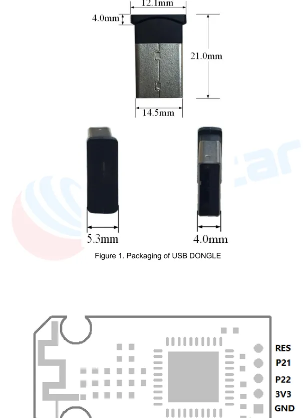
2 Packaging Size and Pins
2.1 Packaging Size
Figure 1. Packaging of USB DONGLE
2.2 Pins
3 RF Test
3.1 Frequency Range Test conditions: VDD = 3.3 V, TA = 25 °C, frequency = 2405 MHz / 2440 MHz / 2480 MHz, RBW = 100 K, VBW = 300 K. Frequency Range 2402 MHz ~ 2480 MHz 3.2 Tx Power Test conditions: VDD = 3.3 V, TA = 25 °C, frequency = 2405 MHz / 2440 MHz / 2480 MHz, RBW = 100 K, VBW = 300 K.Center Frequency (MHz) Tx Power (dBm) Power Range (dBm)
2402 3.3 >2.5 2440 3.42 2480 2.96 3.3 Frequency Offset Test conditions: VDD = 3.3 V, TA = 25 °C, frequency = 2405 MHz / 2440 MHz / 2480 MHz, RBW = 100 K, VBW = 300 K.
Center Frequency (MHz) Frequency Offset (KHz) Offset Range (KHz)
2402 12.3
±40 KHz
2440 12.3
2480 12.3
3.4 Receiving Sensitivity (High Gain Mode, Packet Loss Rate FER = 1%)
Test conditions:
VDD = 3.3 V, TA = 25 °C, frequency = 2405 MHz / 2440 MHz / 2480 MHz, RBW = 100 K, VBW = 300 K, Smart RF studio 7.
Center Frequency (MHz) Receiving Sensitivity (dBm) Sensitivity Range (dBm)
2402 -87
< -85
2440 -88
2460 -89
4 Test Parameters of Key Certificates
4.1 CE Out-of-Band Spurious Limit of Conducted Harmonic
Test conditions:
VDD = 3.3 V, TA = 25 °C, frequency = 2405 MHz / 2440 MHz / 2480 MHz, RBW = 100 K, VBW = 300 K. According to CE Standard EN300328 V1.8.1.
Band
Frequency (MHz) Level (dBm) Standard Unit
Record (Max) level /dBm EN300 328 Spec RBW / VBW
30 MHz ~ 47 MHz 32 -44 -36 100k / 300k 47 MHz ~ 74 MHz 64 -68 -54 100k / 300k 74 MHz ~ 87.5 MHz 75 -57 -36 100k / 300k 87.5 MHz ~ 118 MHz 96 -66 -54 100k / 300k 118 MHz ~ 174 MHz 128 -53 -36 100k / 300k 174 MHz ~ 230 MHz 192 -65 -54 100k / 300k 230 MHz ~ 470 MHz 256 -60 -36 100k / 300k 470 MHz ~ 862 MHz 480 -71 -54 100k / 300k 862 MHz ~ 1 GHz 7215 -61 -36 100k / 300k 1 GHz ~ 2.36 GHz 7350 -42 -30 1M / 3M 2.5235 GHz ~ 12.75 GHz 7440 -58 -30 1M / 3M
4.2 FCC Out-of-Band Spurious Limit of Conducted Harmonic
Test conditions:
VDD = 3.3 V, TA = 25 °C, frequency = 2405 MHz / 2440 MHz / 2480 MHz, RBW = 100 K, VBW = 300 K. According to FCC Standard part 15.247.
Carrier Frequency (MHz)
Harmonic Frequency (MHz))
FCC requirements: <-41.2 dBm
Actual Measurement (dBm) Allowance (dB) 2402 4810 -52.5 11 7215 -60.4 19 9620 -63.1 22 2440 4880 -55.8 14 7320 -61.7 20 9760 -60.5 19 2480 4960 -55.3 14
7440 -64.5 23
9920 -67.2 26
4.3 Test Results of FCC and CE Radiation Spurious
Test conditions:
VDD = 3.3 V, TA = 25 °C, frequency = 2405 MHz / 2440 MHz / 2480 MHz, RBW = 100 K, VBW = 300 K. According to FCC Standard part 15.247 and CE Standard EN300328 V1.8.1.
Requirements: Peak Detector <74 dBuV/m @ 3 m, Average Detector <54 dBuV/m @ 3 m.
Carrier Frequency (MHz)
Harmonic Frequency (MHz))
Peak (dBuV) Average (dBuV) Peak Detector Average Detector 2402 4810 62.5 48.6 7215 64.7 46.9 9620 63.2 48.5 2440 4880 61.4 49.1 7320 62.5 46.8 9760 63.4 46.9 2480 4960 61.7 46.3 7440 63.8 47.2 9920 65.3 47.6
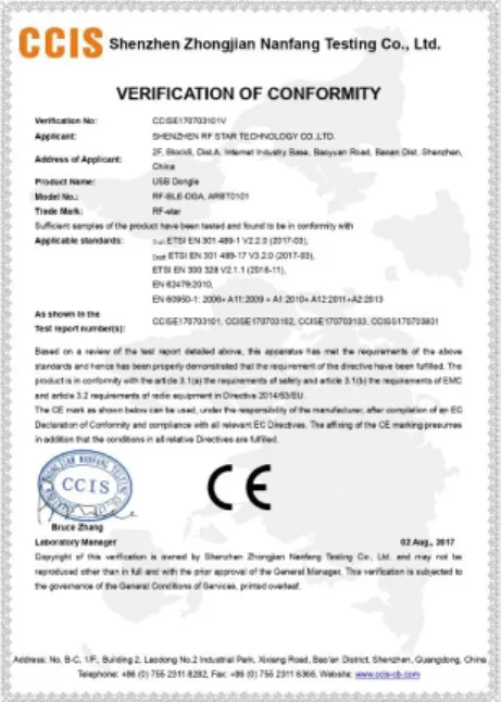
5 Antenna Gain Pattern
5.1 Antenna Information
Antenna type: PCB antenna
Figure 3. Antenna Picture of USB DONGLE
5.2 Antenna Radiation Pattern
Figure 4. Antenna Radiation Pattern of USB DONGLE
5.3 Antenna Radiation Gain
Radiation Pattern
Plane Frequency (MHz) Max. Value (dB) Average (dB) ZX 2400 0.22 -3.47 2450 0.22 -3.71 2500 0.03 -3.86 ZY 2400 0.97 -2.33 2450 1.06 -2.15 2500 0.85 -2.17
XY
2400 -0.62 -4.55
2450 -0.83 -4.74
6 Application, Implementation, and Layout
6.1 Block Diagram
Figure 5. Block Diagram of RF-BM-S01
6.2 Schematic Diagram
Figure 6. Schematic Diagram of USB DONGLE
CC2540F256 USB Interface LC Balun PCB Antenna RF-N RF-P
High Pass Filter & Matching 32.0 MHz
LDO, Power Filter
7 Instruction for Use
7.1 Software Preparation
Download TI BTool.
Download address: https://www.szrfstar.com/download/593-cn.html
7.2 Transparent Transmission Function Test
1. Power on the module with the voltage of 3.0 V ~ 3.3 V, plug the USB Dongle into the USB port of PC. Then, a serial port device (such as: COM3) will show in the hardware management.
3. Open BTooL: Device---New Device, choice the founded serial port and the default settings, press “OK”.
5. Connect the defined device.
7. Choose Discover Characteristic by UUID.
8. Write E4:FF to Characteristic UUID, press Read, and the Value column appears 10 0E 00 E4 FF, wherein 10 represents the permission, 0E 00 means handle 0x000E with the lower bit in the front. E4 FF means UUID with the lower bit in the front.
Since the handle value is 00 0E, 1 needs to be added to the handle, so write 0x000F in Characteristic Value Handle. Then write 01:00 to Handle:0x000F to enable the automatic notify switch of the serial data channel, as shown in the figure below. If the master sends a legitimate data packet to the RX of the BLE module, the module will automatically send it to BTool in the form of a notify, and the display column on the left will show the specific data. The data sent by the MCU to the module can be any length within 200 bytes.
Next, perform a write operation on the module, write E9:FF to Characteristic UUID, press Read, and the value column appears 0C 13 00 E9 FF, wherein 0C represents the permission, 13 00 means handle 0x0013 with the lower bit in the front, E9 FF means UUID with the low order in the front.
9. It can be seen from the above figure that handle is 0x0013. Because the data from the slave to the master is set, there is no need to add 1 to the handle. Write 1 byte ~ 20 bytes of data to the module through BTool. When the module receives a write operation from BTool, the module will send it to the MCU through the serial port. The user can check whether the data is correct by reading the MCU, or display the data written by BTool to the module through the UART Assistant.
10. UART Assistant received the data written by BTool.
7.3 Direct-Driven Function Test
Any channel defined by the protocol can be visited by BTool and USBDongle. The typical steps are as follows: 1. Find the handle of channel through UUID.
2. Remember the corresponding handle of the channel. 3. Turn on the channel notify switch by handle+1. 4. Read the channel by UUID or handle.
5. Write the channel by handle.
If directly use the handles provided in the characteristic list of “BLE Protocol (APP Interface)”, Step 1 and 2 can be skipped. Notify switch of channels must be conducted by handle+1 indicator. The so-called “channel” here refers to the (Characteristic) value. When writing a channel, the byte number must be consistent with the length defined by the Protocol, or it will be regarded as illegal and fail data.
Important Notice: The key operation with BTool is the 3 steps: first connect, then read and write the handle of certain channel, and turn on the notify switch afterwards. Step 1 & 2 are to find the corresponding handle. But in iOS programming, there is no need to look for the handle. Read and write can be done through the channel UUID directly.
Now take the example of ADC to illustrate how to use the USB Dongle and BTool to directly drive the Bluetooth module. The module type in the following example is BLE transparent transmission module V2.23u of RF-star. Its handle may be of a little difference from other versions. But the operation process is exactly the same. Other test methods are similar. They just have different channel UUID, but have the same way of read and write.
ADC input (2 Channel) 【Service UUID: 0xFFD0】
Characteristic UUID Operation Bytes Default Value Remarks FFD1
(handle:0x0036)
Read /
Write 1 0x00
Enable control
0x00: Close 2 ADC channels 0x01: Open ADC0 channel 0x02: Open the ADC1 channel 0x03: Open two ADC channes.
FFD2 (handle:0x0039)
Read /
Write 2 0x01F4
Sampling cycle (ms)
For example: 0x01F4 is corresponding to 500 ms.
FFD3 (handle:0x003C)
Read /
Notify 2 0x0000 ADC0 sampling result: maximum to be 0x01FFF
FFD4 (handle:0x0040)
Read /
Notify 2 0x0000 ADC1 sampling result: maximum to be 0x01FFF
Remark: 2-channle ADC input control. APP operates write in this channel FFD1 by BLE API to open two 13-bit ADC channels. Sampling cycle t (in ms, t 100 ms) of two ADC channels is controlled by write in FFD2 channel. If notify of FFD3 and FFD4 is enabled (01 00 is needed to write to 0x003C+1 = 0x003D and 0x0040+1 = 0x0041 by BTool), a notify event with sampling results (0 ~ 0x1FFF, low byte in front) will come in this channel after the sampling results are generated. Those sampling results can be processed and used by the APP in the callback function of notify. ADC
reference power supply is the chip internal reference power supply of 1.25 V. So, the flotation of the voltage of power supply will not lead to any new measurement errors, but the sampling voltage measured must be controlled between 0 V ~ +1.25 V.
1. Open ADC0 and ADC1. And the subsequent operations can be done in the order of what the red arrow directs (as shown below). First is to find the UUID that needs to be controlled. Input the UUID with lower byte in the front (D1:FF) and read. After read is successful, get handle=0x0036. Write 03 to 0x0036 will open ADC0 and ADC1 (see the table above).
2. Read and reset the sampling cycle. First to read FFD2 channel and get 01 F4, which means the default value is 500 ms. Get handle=0x004A and write 02 00 (higher byte in the front) to the handle. And the sampling cycle will be set at 512 ms (0x0200 = 512 ms).
3. Enable notify switch of ADC0. The address of notify switch is handle+1, 0x003C+1=0x003D. Since then, the ADC0 sampling cycle for each time is different from the last time one, otherwise, there will a new notification.
4. Enable notify switch of ADC1. The address of notify switch is handle+1, 0x0040+1=0x0041. Since then, the ADC1 sampling cycle for each time is different from the last time one, otherwise, there will a new notification.
8 Certification
8.1 FCC
This device complies with part 15 of the FCC Rules. Operation is subject to the following two conditions: (1) This device may not cause harmful interference, and (2) this device must accept any interference received, including interference that may cause undesired operation.
FCC Identifier: Q9DBT101
Figure 7. FCC Certificate
8.2 CE
CE Verification No.: CCISE170703101V
7.3 RoHS
RoHS Report No.: CSC1403200001CHEM
Figure 9. RoHS Certificate
7.4 IC
IC Verification ID: CCIS14110091401V
9 Revision History
Date Version No. Description 2017.02.20 V1.0 The initial version is released.
2020.08.07 V1.0 Update some parameters. Note:
1. The document will be optimized and updated from time to time. Before using this document, please make sure it is the latest version.
10 Contact Us
SHENZHEN RF-STAR TECHNOLOGY CO., LTD. Shenzhen HQ:
Add.: Room 601, Block C, Skyworth Building, High-tech Park, Nanshan District, Shenzhen, Guangdong, China Tel.: 86-755-3695 3756
Chengdu Branch:
Add.: No. B3-03, Building No.1, Incubation Park, High-Tech District, Chengdu, Sichuan, China, 610000 Tel.: 86-28-6577 5970
Email: [email protected], [email protected] Web.: www.szrfstar.com