462
Copyright © 2016. Vandana Publications. All Rights Reserved.
Volume-6, Issue-5, September-October 2016
International Journal of Engineering and Management Research
Page Number: 462-469
Performance Analysis of Combined (ZVS, ZCS) DC-DC Converter
Mohammed Zaheer Khan1, G.Kishor2
1,2Department of EEE, GPREC, INDIA
ABSTRACT
This paper presents a Hybrid Switching step-down DC/DC converter with isolation between line and source using a transformer. This converter provides a wide range of Z.V.S and Z.C.S which is zero voltage switching for the leading switches in inverter circuit and zero current switching for lagging switches in the inverter circuit. A combination of ZVS and ZCS is used to avoid freewheeling circulating losses in primary side. Since the Voltage across the Resonating Capacitor is applied between bridge rectifier and output inductor for freewheeling interval, due to which a small size output inductor can be used. By providing a clamping path to the current rectifier of combined Switching circuit, eliminating the voltage overshoots that arise during turn-OFF of Rectifier diodes. The effectiveness of H.S.P.S.F.B DC-DC converter is verified using MATLAB simulation tool.
Keywords— ZVS, ZCS, DC-DC converter
I.
INTRODUCTION
Hybrid Electric Vehicles uses battery packs with high energy density to store energy. These are charged using AC/DC charger which includes front-end power factor corrector followed with an isolated DC/DC converter. The PFC improves the quality of input current, whereas converter provides isolation between utility and charges High-voltage battery pack [1]-[8]. In ZVS Phase-Shift full bridge DC/DC converter [1], all the switches are operated in ZVS condition. At light load conditions the lagging leg switches tend to lose ZVS ability. Since ZVS of lagging leg switches is obtained by energy stored in leakage inductance [3]. The limitations of PSFB DC-DC converter is studied in [4]. Comparison of full bridge and two inductor boost converter systems [10].
II.
COMBINED (ZVS, ZCS) DC/DC
CONVERTER
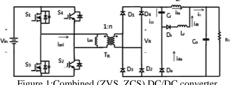
Combined (ZVS, ZCS) DC/DC converter [4] is shown in Fig:(1). This converter is derived from a non- isolated hybrid-switching step-down DC/DC converter which belongs to a category of switching converters named hybrid-switching converters introduced by Cuk [5-6]. This HSSD DC/DC converter is characterized by hybrid resonant and PWM waveforms of current and voltages. The charge balance of resonant capacitor is satisfied by hybrid linear PWM current and sinusoidal resonant current, this conversion leads to leads to reduced voltage stress on switches compared to PWM converters operating at same duty ratio.
The ZVS, ZCS converter transfers energy from input to output simultaneously stores energy in resonant capacitor and output inductor during S1 and S2 intervals whereas during freewheeling intervals this stored energy is supplied to load through single diode which is in series with the current path, and provides effective and efficient energy transfer. Resonating capacitor and output inductor discharging at start of freewheeling period provides additional current to assist leading leg switches and resets primary current to zero instantly. This results a wide range of ZVS to leading-switches and ZCS to lagging-switches at switch Turn-OFF states [4].
Figure 1:Combined (ZVS, ZCS) DC/DC converter
463
Copyright © 2016. Vandana Publications. All Rights Reserved.
arise during turn-Off of output diodes in conventional PSFB DC/DC converter are eliminated and voltage stress on bridge rectifier diodes are well clamped on secondary-reflected input voltage and provides enhanced reliability[4].
ZVS, ZCS DC/DC converter has a simple structure, physically smaller output inductor with minimized voltage stress across rectifier and high efficiency over wide output power and voltage ranges, because of these characteristics it is suitable for electric vehicles. The analysis on performance of ZVS, ZCS DC/DC converter at various line voltages, load conditions is presented
III.
HSSD BASIC OPERATION
Using the Hybrid-Switching method an extra capacitive energy is stored and transfer from input to output, this minimizes the voltage stress and switching losses of the switches. The on time is always equal to half of the resonant period [5-6].
(1)
Switch Turn-ON interval:
• output inductor and resonant capacitor stores
energy.
• Power is supplied to load with combined resonant
and PWM currents Switch Turn-OFF interval:
• Capacitive (resonant capacitor) and output
inductor energies are transferred to loads.
IV. OPERATING MODES OF
COMBINED (ZVS, ZCS) DC/DC
CONVERTER
High efficiency combined (ZVS, ZCS) DC/DC converter is achieved by introducing a isolation transformer and applying PWM control technique to a HSSD presented in [5-6] .The wide range of output voltage can also be regulated using customary phase-shift PWM control with stable switching frequency. Multi-phase boost converter with reduced input current ripples [11].
The resonant inductor can be removed in favor of using leakage inductor Llr of a transformer to resonate with
resonant capacitor which reduces number of components required.
IGBT’s are used instead of MOSFET’s in lagging legs in favor of ZCS since the tailed-current persuaded losses of IGBT’s are minimized with zero current turn -OFF.
Conventional phase-shift PWM control with fixed switching frequency and variable duty ratio is applied to combined (ZVS, ZCS) converter. It operates in three modes as in designed [6].
(3)
(4)
Where ‘n’ is transformation constant
TABLE 1
Switching Time For Different Modes
MODE 1 MODE 2 MODE 3
TActive>Tr TActive=Tr TActive<Tr
The switching times for different modes of operation are as given in Table 1. These modes can be distinguished by resonant current through Dr. in mode 1
idr reaches zero before converter arrives freewheeling
interval. In mode-2 idr reaches zero instant where converter
reaches freewheeling. Where as in mode-3 idr is more than
zero and interrupted at instant converter enters freewheeling.
A. MODE 1 (TActive > Tr )
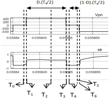
The key waveforms for the combined ZVS and ZCS DC/DC converter are as shown in Fig2. The different modes of operation with different stages are discussed as shown in Fig.3.
Stage 1 [To,T1]
Since secondary current isec < output inductor current, diode Do is kept ON and the energy stored in Cr is
passed to output until isec = ilo
Stage 2 [T1,T2]
At t1 isec > ilo, diode Do is reverse biased and Dr
is ON. Lr starts to resonate with Cr and transfers energy
from input to output.
464
Copyright © 2016. Vandana Publications. All Rights Reserved.
Stage 3 [T2,T3]
At, Idr resonates to zero and diode Dr is OFF with
zero current, but energy is transfers from input to output using transformer Tr with isec equal to ilo.
Stage 4 [T3,T4]
At T3, S1 is OFF the ipri starts to charge and
discharge the junction capacitors of leading-leg switches when drain-source voltage of S3 reaches zero ipri flows
through body diode of S3 after dead time S3 is turned with ZVS.
Stage 5 [T4,T5]
At T4 isec < ilo making Do forward bias, Vcr is
applied across bridge rectifier. As a result Ipri quickly resets to zero and offer ZCS turn-OFF for lagging switches.
Stage 6 [T5,T6]
isec , ipri reduced to zero and stored energies in Cr
and Lo are passed through D0 to output until S4 turns-ON
at T6.
As Cr voltage is always higher than zero the
bridge rectifier is reverse biased by Cr and never conducts
during freewheeling period. .
Stage 1
Stage 2
Stage 3
Stage 4
Stage 5
Stage 6
Figure 3: Topological stages of combined (ZVS,ZCS) DC/DC converter
B. Mode 2 (TActive = Tr )
Main difference in this mode compared to mode-1 is stage 3 of mode-1 does not happen in this as switch S1 is
OFF at instant idr reaches zero.
C. Mode 3 ( TActive < Tr)
As the Tr period is resonant circuit is longer than
active interval idr is higher than zero and resonance is
stopped at T3. Stages (1,2) are as same as mode-1
Stage 3[T2,T3]
At T2 S1 is OFF ipri (reflected output inductor
current n*ilo and reflected resonant current*idr), starts
through junction capacitors of S1 and S3. When
drain-source voltage of S3 reaches zero, ipri flows through body
diode of S3. After dead time S3 is turned ON with ZVS.
V.
RESULTS AND OBSERVATIONS
The converter is operated at different line voltages, and different loads. The isolation transformer used has the turns ratio of 29:34. Results with observations for each mode are presented below.
MODE 1 (TActive > Tr
In this mode the resonating current i
):
dr reaches
465
Copyright © 2016. Vandana Publications. All Rights Reserved.
Load Regulation is performed at different load conditions and values are tabulated. The response of the converter for different modes is shown below Fig.4 and Fig.5.
Figure 4: Transformer Primary voltage (Vpri), Secondary
voltage, Output Inductor Current, Resonating diode current, Resonating Capacitor Current, Resonating Capacitor Voltage, Output Diode Current, Output Current, Output Voltage of the converter operating at 400V input and 150Ωload
Figure 5: Transformer Primary voltage, Secondary voltage, Output Inductor Current, Resonating diode current, Resonating Capacitor Current, Resonating Capacitor Voltage, Output Diode Current, Output Current, Output Voltage of the converter operating at 400V input and 195Ωload
MODE 2 (TActive=Tr ):
In mode 2 operation the resonant current idr
466
Copyright © 2016. Vandana Publications. All Rights Reserved.
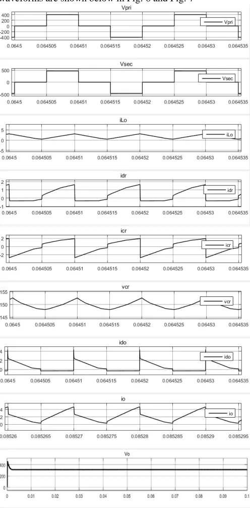
resonating time periods are the same both are equal. The converter is operated at different line voltages and achieved 97.68% of efficiency. At the different load conditions and at different line voltages the respective waveforms are shown below in Fig: 6 and Fig: 7
Figure 6: Transformer Primary voltage, Secondary voltage, Output Inductor Current, Resonating diode current, Resonating Capacitor Current, Resonating Capacitor Voltage, Output Diode Current, Output Current, Output Voltage of the converter operating at 400V input and 150Ω load
Figure 7: Transformer Primary voltage, Secondary voltage, Output Inductor Current, Resonating diode current, Resonating Capacitor Current, Resonating Capacitor Voltage, Output Diode Current, Output Current, Output Voltage of the converter operating at 400V input and 195Ω load
MODE 3 (TActive<Tr):
In mode 3 operation the resonant current idr higher
467
Copyright © 2016. Vandana Publications. All Rights Reserved.
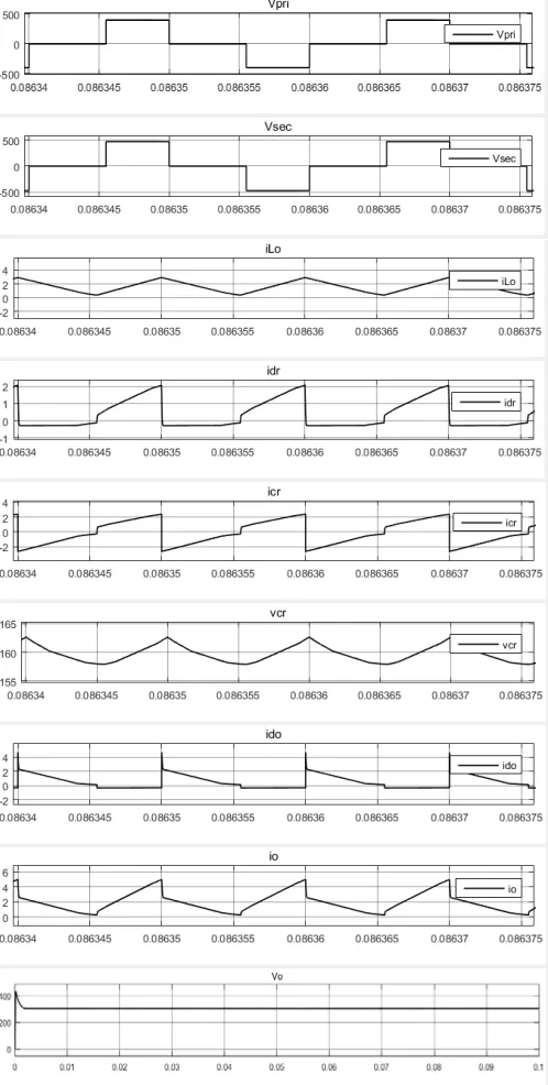
is operated at different line voltages achieved 93.56% of efficiency. At the different load conditions and at different line voltage conditions the respective waveforms are shown below in Fig: 8 and Fig: 9
Figure 8: Transformer Primary voltage, Secondary voltage, Output Inductor Current, Resonating diode current, Resonating Capacitor Current, Resonating Capacitor Voltage, Output Diode Current, Output Current, Output Voltage of the converter operating at 400V input and 150Ω load
Figure 9: Transformer Primary voltage, Secondary voltage, Output Inductor Current, Resonating diode current, Resonating Capacitor Current, Resonating Capacitor Voltage, Output Diode Current, Output Current, Output Voltage of the converter operating at 400V input and 195Ω load.
468
Copyright © 2016. Vandana Publications. All Rights Reserved.
MODE 1 (TActive>Tr ):
Table 2 shows load Vs. efficiency of the converter in Mode 1. The graph for the load Vs. efficiency is as shown in Figure (10)
TABLE 2
LOAD VS.EFFICIENCY IN MODE 1
LOAD Ii Vo Io Po Pi Efficiency
150 4.209 375.1 4.311 1617 1684 96.02
195 3.588 381.9 3.245 1239 1435 86.34
240 3.186 390.2 2.765 1079 1274 84.64
285 2.894 398.1 2.443 972.5 1158 84
Figure 10: Load Vs Efficiency Graph
Tabular column and plot shows the load v/s efficiency analysis the load is increased by 30% at each stage and obtained a power output of 1.617Kw at 375.1V outout voltage and the max efficiency of 96.02%.
Table 3 shows line voltage Vs. efficiency of the converter in Mode 1. The graph for the line voltage Vs. efficiency is as shown in Figure (11)
TABLE 3
LINE VOLTAGES VS.EFFICIENCY IN MODE 1
Vin Ii Vo Io Po Pi efficiency
200 2.099 186.8 2.146 400.7 419.8 95.45
300 3.154 280.9 3.227 906.6 946.3 95.8
400 4.209 375.1 4.311 1617 1684 96.02
Figure 11: Line Voltage Vs Efficiency Graph
The tabular column shows the increse in efficiency of 96.02% at 400V and 95.45% at 200V of input dc voltage. The efficiency is maintained at 95% to 96% for 200V to 400V there exists a efficient performance of the dc/dc converter.
Table 4 shows Load Vs. efficiency of the converter in Mode 2. The graph for the load Vs. efficiency is as shown in Figure (12)
Table 4 and plot shows the load v/s efficiency analysis the load is increased by 30% at each stage and
obtained a power output of 1.49KW at 314 output voltage. And the efficiency is 97.68% at 314 output voltage.
TABLE 4
LOAD VS.EFFICIENCY IN MODE 2
LOAD Ii Vo Io Po Pi Efficiency
150 3.812 314 4.744 1490 1525 97.68
195 3.273 321.4 3.766 1210 1309 92.45
240 2.937 329.4 3.198 1054 1175 89.68
285 2.697 337.3 2.802 945 1079 87.59
Figure 12: Load Vs Efficiency Graph
Table 5 shows Line Voltage Vs. efficiency of the converter in Mode 2. The graph for the line voltage Vs. efficiency is as shown in Fig.13
TABLE 5
LINE VOLTAGE VS.EFFICIENCY IN MODE 2
Vin Ii Vo Io Po Pi efficiency
200 1.9 156.3 2.362 369 380 97.11
300 2.856 235.1 3.552 835.3 856.8 97.49
400 3.812 314 4.744 1490 1525 97.68
Figure 13: Line Vs Efficiency Graph
Table 5 shows the increse in efficiency of 97.11% at 200V and 97.11% at 200V of input dc voltage. The efficiency is maintained at 97% for 200V to 400V there exists a efficient performance of the dc/dc converter.
Table 6 shows Load Voltage Vs. efficiency of the converter in Mode 3. The graph for the line voltage Vs. efficiency is as shown in Figure (14)
Table 6 shows the load v/s efficiency analysis, the load is increased by 30% at each stage and obtained a power output of 1.49KW at 314 output voltage. and the max efficiency is 99.76% at 302V output voltage.
TABLE 6
LOAD VS.EFFICIENCY IN MODE 3
LOAD Ii Vo Io Po Pi Efficiency
150 3.738 302.7 4.927 1491 1495 99.76
195 3.215 310 3.958 1227 1286 95.43
240 2.884 317.7 3.355 1066 1153 92.4
469
Copyright © 2016. Vandana Publications. All Rights Reserved.
Figure 14: Load Vs Efficiency Graph
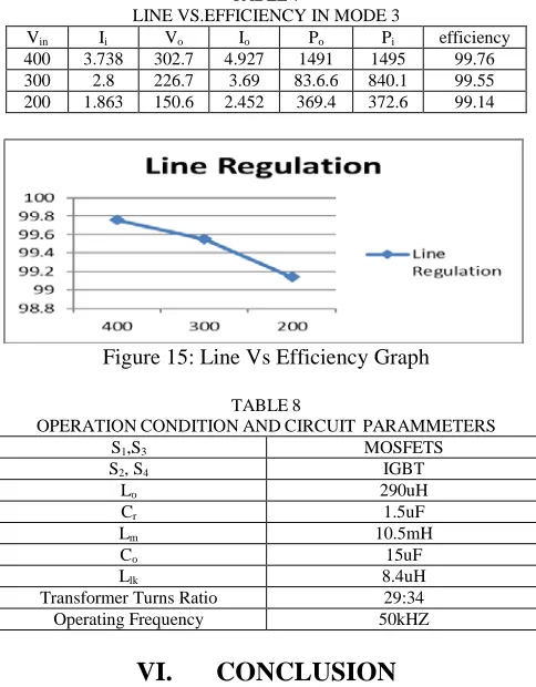
Table 7 shows Line Voltage Vs. efficiency of the converter in Mode 3. The graph for the line voltage Vs. efficiency is as shown in Figure (15).
The table 7 shows the increse in efficiency of 99.76% at 400V and 99.14% at 200V of input dc voltage. The efficiency is maintained at 99% for 200V to 400V there exists a efficient performance of the dc/dc converter.
TABLE 7
LINE VS.EFFICIENCY IN MODE 3
Vin Ii Vo Io Po Pi efficiency
400 3.738 302.7 4.927 1491 1495 99.76
300 2.8 226.7 3.69 83.6.6 840.1 99.55
200 1.863 150.6 2.452 369.4 372.6 99.14
Figure 15: Line Vs Efficiency Graph
TABLE8
OPERATIONCONDITIONANDCIRCUIT PARAMMETERS
S1,S3 MOSFETS
S2, S4 IGBT
Lo 290uH
Cr 1.5uF
Lm 10.5mH
Co 15uF
Llk 8.4uH
Transformer Turns Ratio 29:34
Operating Frequency 50kHZ
VI.
CONCLUSION
The combined (ZVS and ZCS) DC-DC converter is derived by introducing an isolation transformer in hybrid switching step-down converter. This converter exhibits a wide range tor ZVS at turn-ON of leading switch and ZCS at turn-ON of the lagging switch. While transferring the energy in freewheeling period to the output, the energy is the combination of energy at resonating capacitor and PWM power conversion. As the resonant capacitor voltage supplied to output inductor during freewheeling state the
output filter inductance can be reduced and lesser size can be used. The performance analysis of combined (ZVS, ZCS) DC/DC converter are verified with MATLAB simulation.
REFERENCES
[1] K. Morrow, D. Karner, J. Francfort, “Plug-in hybrid electric vehicle charg-ing infrastructure review,” Vehicle Technologies Program, U.S. Depart-ment of Energy, Wahington, DC, 2008.
[2] H. Bai and C. C. Mi, “Comparison and evaluation of different DC/DC topologies for plug-in hybrid electric vehicle chargers,” Int. J. Power Electron., vol. 4, no. 2, pp. 119–133, 2012.
[3] J. A. Sabate, V. Vlatkovic, R. B. Ridley, F. C. Lee, and B. H. Cho, “De-sign considerations for voltage high-power full-bridge zero-voltage-switched PWM converter,” in Proc. Appl. Power Electron. Conf, 1990,
[4] Bin Gu, Jih-Sheng Lai, Nathan Kees, and Cong Zheng, “Hybrid-Switching Full-Bridge DC-DC Converter With Minimal Voltage Stress of Bridge Rectifier, Reduced Circulating Losses, and Filter Requirement for Electric Vehicle Battery Chargers,” in IEEE Transactions on Power Electronics, VOL. 28,NO.3, March 2013.
[5] S. Cuk, “Step-down converter having a resonant inductor, a resonant ca-pacitor and a hybrid transformer,” U.S. Patent 7 915 874, Mar. 2011.
[6] S. Cuk, Z. Zhang, “Voltage step-up switching DC-to-DC converter field of the invention,” U.S. Patent 7 778 046, Aug. 2010.
[7] M. Pahlevaninezhad, P. Das, J. Drobnik, P. K. Jain, and A. Bakhshai, “A novel ZVZCS full-bridge DC/DC converter used for electric vehicles,” IEEE Trans. Ind. Electron., vol. 27, no. 6, pp. 2752–2769, Jun. 2012.
[8] D. Gautam, F. Musavi, M. Edington, W. Eberle, and W. G. Dunford, “A zero voltage switching full-bridge DC-DC converter with capacitive output filter for a plug-in-hybrid-electric vehicle battery charger,” in Proc. IEEE Appl. Power Electron. Conf, Feb. 2012, pp. 1381–1386. [9] T. T. Song and N. Huang, “A novel zero-voltage and zero-current-switching full bridge PWM converter,” IEEE Trans. Power Electron., vol. 20, no. 2, pp. 286–291, Mar. 2005.
[10] G.Kishor, D.Subbarayudu and S.Sivanagaraju,, “Comparison of Full Bridge and two inductor Boost Converter systems”, Journal of Theoritical and information thecnology Vol.34(2), pp.118-124 Dec-2011.