FPGA Implementation of Cryptographic
Algorithm in a Multiprocessing System
S.Priya, Swetha Abraham
M.E (VLSI Design), Department of ECE, Karpaga Vinayaga College of Engineering and Technology,
Madhuranthagam, Tamil Nadu, India
*
Assistant Professor, Department of ECE, Karpaga Vinayaga College of Engineering and Technology,
Madhuranthagam, Tamil Nadu, India.
ABSTRACT: In this paper the AES algorithm has been developed using basic mathematical data encryption algorithm using encryption and decryption. The algorithm is to implement in the multiprocessing system. Multiprocessors have been widely used in modern high performance embedded system to meet the computational needs of smart, real time applications spread across multiple domains. Advanced encryption algorithm implementation involves exhaustive data processing done over multiple steps. These operations include add round key, substitute bytes, shift rows, mix columns. The code is written in Impulse C and implemented in FPGA to obtain the results. The synthesis is done in Xilinx Platform Studio to verify the various parameters used in the system.
KEYWORDS: Multiprocessing, Advanced Encryption Algorithm (AES), Encryption , Decryption, Xilinx Platform Studio(XPS) and FPGA.
I. INTRODUCTION
A. MULTIPROCESSING
Multiprocessing is a general term that can mean the dynamic assignment of a program to one of two or more computers working in tandem or can involve multiple computers working on the same program at the same time (in parallel). With the advent of parallel processing, multiprocessing is divided into symmetric multiprocessing (SMP) and massively parallel processing (MPP). In symmetric (or "tightly coupled") multiprocessing, the processors share memory and the I/O bus or data path.
A single copy of the operating system is in charge of all the processors. SMP, also known as a "shared everything" system, does not usually exceed 16 processors. In massively parallel (or "loosely coupled") processing, up to 200 or more processors can work on the same application. Each processor has its own operating system and memory, but an "interconnect" arrangement of data paths allows messages to be sent between processors. Typically, the setup for MPP is more complicated, requiring thought about how to partition a common database among processors and how to assign work among the processors. An MPP system is also known as a "shared nothing" system. Multiprocessing should not be confused with multiprogramming, or the interleaved execution of two or more programs by a processor. Today, the term is rarely used since all but the most specialized computer operating systems support multiprogramming. Multiprocessing can also be confused with multitasking, the management of programs and the system services they request as tasks that can be interleaved, and with multithreading, the management of multiple execution paths through the computer or of multiple users sharing the same copy of a program.
II. TRIPLE DATA ENCRYPTION ALGORITHM
brute force attacks; Triple DES was designed to provide a relatively simple method of increasing the key size of DES to protect against such attacks, without designing a completely new block cipher algorithm.
K1 K2 K3
P A B C
(a) Encryption
K1 K2 K3
C B A P
(b) Decryption
Fig 2.1 Triple Data Encryption Algorithm
Figure 2.1 represents the basic block diagram of the system. In this project a TDEA algorithm is introduced for data encryption and decryption procedures. Here E and D are represents the encryption and decryption process respectively. A and B represents the output of the encryption and decryption process. In the encryption process, the plaintext (P) is given to the input and the ciphertext (C) is obtained as the output. Key K1=K3 is given to the encryption
block and key K2 is given to the decryption block. It is the same for decryption process. Given below is a detailed
description for each block given in the Figure 3.1.
A. TDEA FORWARD AND INVERSE CIPHER OPERATION
A TDEA consists of three keys for the cryptographic engine (K1, K2 and K3); the three keys are also referred to as a
key bundle (KEY). Two options for the selection of the keys in a key bundle are approved. The following operations are used.
1. TDEA forward cipher operation: the transformation of a 64-bit block d into a 64-bit block Othat is defined as follows:
O = FK3(IK2 FK1 d ) ………….(2.1)
2. TDEA inverse cipher operation: the transformation of a 64-bit block dinto a 64-bit block Othat is defined as follows:
O = IK1(FK2 IK3 d ) ……….(2.2)
Let FKX(d) and IKX(d),respectively, represent the DEA forward and inverse transformations on data d using key
bundle KEY.
1) DES ENCRYPTION
As with any encryption scheme, there are two inputs to the encryption function: the plaintext (P) to be encrypted and the key (K1=K3). In this case, the plaintext (P) must be 64 bits in length and the key is 56 bits in length. The processing
of the plaintext proceeds in three phases. First, the 64-bit plaintext passes through an initial permutation (IP) that rearranges the bits to produce the permuted input. This is followed by a phase consisting of 16 rounds of the same function, which involves both permutation and substitution functions. The output of the last (sixteen) round consists of 64 bits that are a function of the input plaintext (P) and the key. The left and right halves of the output are swapped to produce the preoutput. Finally, the preoutput is passed through a permutation (IP-1) that is the inverse of the initial permutation function, to produce the 64-bit ciphertext (C). With the exception of the initial and final permutations, DES has the exact structure of a Feistel cipher. The right-hand portion shows the way in which the 56-bit key(K) is used.
E D
E
Initially, the key is passed through a permutation function. Then, for each of the 16 rounds, a subkey (ki) is
produced by the combination of a left circular shift and a permutation
.
The permutation function is the same for each round, but a different subkey is produced because of the repeated shifts of the key bits.2) DES DESCRYPTION
The decryption process with DES is essentially the same as the encrypt process and use the ciphertext as the input to the DES algorithm but use the keysKi in reverse order. That is, use K16on the first iteration, K15on the second
until K1 which is used on the 16th and last iteration. The ciphertext (C) must be 64 bits in length and the key is 56 bits
in length. The processing of the ciphertext proceeds in three phases. First, the 64-bit ciphertext passes through an initial permutation that rearranges the bits to produce the permuted input. This is followed by a phase consisting of 16 rounds of the same function, which involves both permutation and substitution functions. The output of the last round consists of 64 bits that are a function of the input ciphertext (C) and the key. The left and right halves of the output are swapped to produce and are passed through a inverse permutation, to produce the 64-bit plaintext (P).
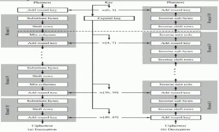
III . ADVANCED ENCRYPTION ALGORITHM
The Rijndael proposal for AES defined a cipher in which the block length and the key length can be independently specified to be 128,,192, or 256 bits. The AES specification uses the same three key size alternatives but limits the block length to 128 bits.
Fig 3.1 AES Encryption and Decryption
column of the in matrix, the second four bytes occupy the second column, and so on. Similarly, the first four bytes of the expanded key, which form a word, occupy the first column of the w matrix.
1) APPLICATION IN MULTIPROCESSING SYSTEM
Figure 3.2 represents the basic block diagram of the multiprocessing system. The input data from the processor P1 to be transferred to P2 is encrypted before entering the bus line. The encrypted data transferred to the
processor P2 after reception is decrypted to retrieve the original data.
This cryptographic procedure is done using the proposed TDEA algorithm. Thus safe and error free data transfer is done in the multiprocessing system.
Data transfer
Fig 3.2 Multiprocessing system
IV. SIMULATION RESULTS
Xilinx Platform Studio (XPS) is a key component of the ISE Embedded Edition Design Suite, helping the hardware designer to easily build, connect and configure embedded processor-based systems; from simple state machines to full-blown 32-bit RISC microprocessors systems.
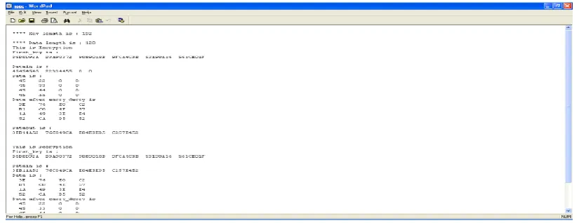
Fig 4.1 Output window for AES algorithm
Figure 4.1 shows the implemented output in hyperterminal. The code is compiled and checked for errors. Then implementation is started by adding file to the work library and adding all signals to wave. Thereby the output window in which the AES algorithm has been detected is displayed.
In encryption process, the plaintext (input) 45454545 22334455 0 0, key D5D0D92A D3A90372 9089018B 9FCA4C3B 53198A16 561CE01F is given to the algorithm. So the ciphertext (output) 3EB11A52 76C049CA E04E3ED5 C257E452 is obtained.
P1 P
In decryption process, the ciphertext (input) 3EB11A52 76C049CA E04E3ED5 C257E452, key D5D0D92A D3A90372 9089018B 9FCA4C3B 53198A16 561CE01F is given to the algorithm. So the plaintext (output) 45454545 22334455 0 0 is obtained.
COMPARISON TABLE 4.1
Resource Type TDEA
Used available %
AES
Used available %
Slices 47834656 102 712 1920 37
4 input LUTs 91209312 97 1377 3840 35
IOs 256 NA NA 2296 NA NA
Bonded IOBs 240 232 103 0 97 0
V.CONCLUSION
The AES algorithm has been developed using basic mathematical data encryption algorithm using encryption and decryption. The algorithm is to implement in the multiprocessing system. The code is written in Impulse C and implemented in FPGA to obtain the results. The synthesis is done in Xilinx Platform Studio to verify the various parameters used in the system. The present algorithm can be enhanced for meeting high performance levels with modifications in the architectural level.
REFERENCES
[1] Mohammed Ahsan Raza, Syed Azeemuddin(2014), "Multiprocessing on FPGA using Light Weight Processor” IEEE conference on CCT.
[ 2 ] Philippe Bonnot, Fabrice Lemonnier, Gerard Gaillat, Olivier Ruch,Pascal Gauget, Gilbert Edelin" Definition and SIMD implementation of a multi-processing architecture approach on FPGA"Design, Automation and Test in Europe, 2008.
[3] Qian Zhou, Yu-kun Song, Duo-Ii Zhang, Gao-ming Du "A design of Multi-core System Based on Avalon Bus" International Conference on Computer Science and Network Technology 201 1.
[4] Hui Yan Cheah, Suhaib Fahmy, Douglas L. Maskell, "iDEA: A DSP Block Based FPGA Soft Processor", IEEE International Conference on Field Programmable Technology (FPT), Seoul, 2012.
[ 5 ] Ms. Ranjana Sharma, Prof V.V. Joshi, Prof V.M. Rohokale"Performance of Router Design for Network-On-Chip Implementation", "2012 International Conference on Communication, Information & Computing Technology ".
[ 6] William C. Barker, Elaine Barker "Recommendation for the Triple Data Encryption Algorithm (TOEA) Block Cipher" Revised January 2012. [7] R. Yuan, SJ. Ruan, J. Gotze" A Practical NOC Design for Parallel DES Computation", " VLSI Design, Automation, and Test (VLSI-DAT), 2013 "
[ 8] P. Buciak and J. Botwicz, "Lightweight multi-threaded network processor core in FPGA," in Design and Diagnostics of Electronic Circuits and Systems, Apr. 2007, pp. 1-5.