IJEDR1604039 International Journal of Engineering Development and Research (www.ijedr.org) 241
Design of High Step-Up DC-DC Converter with
Single Switch and SPWM Inverter for Micro
source Application
S.Priya, Assistant Professor
Department of EEE, Jeppiaar Institute of Technology, Sriperumbudur, India [email protected]
Abstract
— This paper proposes a new high step-up DC–DC converter designed especially for regulating the dc interface between various micro sources and a dc–ac inverter to electricity grid. The need of Electricity increases the power demand where the power demand met by the conventional sources of energy has some disadvantage of pollution, this disadvantage can be decreased by the use of the Renewable energy sources like Fuel Cell and available solar energy. The figuration of the proposed converter is a quadratic boost converter with the coupled inductor in the second boost converter. The converter achieves high step-up voltage gain with appropriate duty ratio and low voltage stress on the power switch. Additionally, the energy stored in the leakage inductor of the coupled inductor can be recycled to the output capacitor. The inverter is switched with SPWM techniques used to reduce the harmonics and to achieve high-voltage, high-power capability but switching losses are increased because of increased device count. Switching losses can be reduced by Soft switching techniques. To verify the performance of the proposed converter, a 280-W prototype sample is implemented with an input voltage range of 20–40 V and an output voltage of up to 400 V. The upmost efficiency of 93.3% is reached with high-line input; on the other hand, the full-load efficiency remains at 89.3% during low-line input.Index Terms
— High step-up DC-DC converter, SPWM Inverter, micro grid, micro sources.I.
INTRODUCTION
Renewable energy is becoming increasingly important and prevalent in distribution systems, which provide different choices to electricity consumers whether they receive power from the main electricity source or in forming a microsource not only to fulfill their own demand but alternatively to be a power producer supplying a microgrid. A microgrid usually includes various microsources and loads, which operate as an independent and controllable system when they are either grid-connected or islanded, as well as when they can reliably connect or disconnect. The microsource is classified either as a dc source or as a high frequency ac source. These two microsource categories are comprised of diverse renewable energy applications, such as solar cell modules, fuel cell stacks, wind turbines, and reciprocating engines.
A.
Power Electronics Interface:
The study of PE devices, along with their control systems, is a very dynamic discipline. By taking advantage of technological innovations in semiconductor materials, and microprocessor (or digital-based) control systems, PE is creating devices that enhance energy generation and delivery systems. The versatility and reliability of lower cost devices combined with advances in circuit topologies and controls has resulted in technologies that replaced what has been traditionally done by electromagnetic and electromechanical systems. With the development of solid-state-based packages, PE devices can now convert almost any form of electrical energy to a more desirable and usable form. This is why PE-based systems are ideal for DE systems. Another benefit of PE is their extremely fast-response times. PE interfaces can respond to power quality events or fault conditions within in the subcycle range. This speed response can enable advanced applications, such as the operation of intentional islands (microgrids) for high-reliability applications and reducing fault level currents of DG, features that do not exist today.
1) Components of PE:
IJEDR1604039 International Journal of Engineering Development and Research (www.ijedr.org) 242
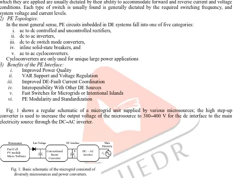
Fig. 1:Basic schematic of the microgrid consisted of diversely microsources and power converters.
i. semiconductor switches,
ii. switch gating and controls systems, iii. inductive components, and iv. capacitive components.
The inductive and capacitive components are used to dynamically store energy for circuit power flow dampening, filtering, and transformation. Switch gating and controls turn ON and OFF the semiconductor devices so that the circuit provides the desired power conversions, ancillary services, and protective functions in an efficient and stable manner.
Innovations and improvements in semiconductor switch designs have been the driving force for the advancements and implementation of PE interfaces. Their operation can be evaluated analogous to a switch, which essentially ―opens‖ or ―closes‖ based on control schemes and circuit conditions. Semiconductor switches and the manner in which they are applied are usually dictated by their ability to accommodate forward and reverse current and voltage conditions. Each type of switch is usually found is generally dictated by the required switching frequency, and system voltage and current levels.
2) PE Topologies:
In the most general sense, PE circuits imbedded in DE systems fall into one of five categories: i. ac to dc controlled and uncontrolled rectifiers,
ii. dc to ac inverters,
iii. dc to dc switch mode converters, iv. inline solid-state breakers, and
v. ac to ac cycloconverters.
Cycloconverters are only used for unique large power applications
3) Benefits of the PE Interface: i. Improved Power Quality
ii. VAR Support and Voltage Regulation
iii. Improved DE-Fault Current Coordination
iv. Interoperability With Other DE Sources
v. Fast Switches for Microgrids or Intentional Islands
vi. PE Modularity and Standardization
Fig. 1 shows a regular schematic of a microgrid unit supplied by various microsources; the high step-up converter is used to increase the output voltage of the microsource to 380–400 V for the dc interface to the main electricity source through the DC–AC inverter.
Both the single solar cell module and the fuel cell stack are essentially low-voltage sources, and thus, a high step-up voltage gain DC– DC converter is required to regulate the voltage of the DC–DC interface.
The various converters for high step-up applications has included analyses of the switched-inductor and switched-capacitor types the boost type integrating with the switched-capacitor technique the voltage-lift type the capacitor-diode voltage multiplier type and the transformer less dc–dc converters. In these converters the voltage gain is not enough to convert to a suitable ac source as a model microsource, in case of extremely high voltage gain is required, to using series connection of converter is able to reach much higher voltage gain. As known, the efficiency and voltage gain of dc–dc boost converter are restrained by either the parasitic effect of power switches or the reverse-recovery issue of diodes. In addition, the equivalent series resistance (ESR) of capacitor and the parasitic resistances of inductor are also affecting overall efficiency. Although an alternative solution is the dc–dc fly back converter along with some advantages such as simple structure, easy control, and cost effective, the energy of leakage inductor of the transformer leads to low efficiency and high-voltage stress across the active switch To employ an active clamp technique not only to recycle the leakage inductor energy of the transformer but to constrain
Fuel Cell PV module Micro Turbines
Conventional Boost Converter
IJEDR1604039 International Journal of Engineering Development and Research (www.ijedr.org) 243
Fig. 2:Proposed Block Diagram
the voltage stress is the crossed active switch, however, the tradeoff is of higher cost and a complex control circuit. Some converters effectively combined both boost and fly back converters as one or other different converter combinations are developed to carry out high step-up voltage gain by using the coupled-inductor technique. Due to voltage gain has restricted by the voltage stress on the active switch, once the leakage inductor energy of the coupled-inductor can be recycled that reduced the voltage stress on active switch, this leads to the coupled inductor and the voltage-multiplier or voltage-lift techniques are successfully accomplished the goal of higher voltage gain.
II.
PROPOSED
METHOD
A. High Step up DC-DC Converter:
The fig 2. presents a cascaded high step-up dc–dc converter to increase the output voltage of the microsource to a proper voltage level for the dc interface through dc–ac inverter to the main electricity grid.
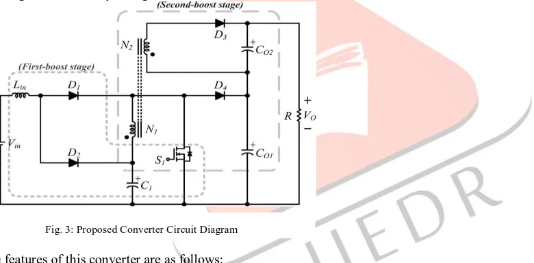
The proposed converter is a quadratic boost converter with the coupled inductor in the second boost converter. The circuit diagram of the proposed converter is shown in Fig. 3; the proposed circuit can be divided as a conventional boost converter and a boost–fly back converter. These two segments are named first boost stage and second boost stage. The first boost stage is like a boost converter that includes an input inductor Lin , two diodes D1 and D2 , and a pumping capacitor C1 . The second boost stage is a boost–fly back converter that includes a dual-winding coupled inductor T1 , two diodes D3 and D4 , and two output capacitors CO1 , and CO2 . In particular, these two stages are driven by a single switch S1.
Fig. 3: Proposed Converter Circuit Diagram
The features of this converter are as follows:
i. The quadratic boost converter is effectively extended to a voltage conversion ratio and the first boost stage also benefited the input current ripple reduction;
ii. The leakage inductor energy of the coupled inductor can be recycled, which reduces the voltage stress on the active switch, and also the conversion efficiency is significantly improved.
The dual-winding coupled inductor consisted of a magnetizing inductor Lm, primary leakage inductor Lk
1 , secondary leakage inductor Lk 2 , and an ideal transformer, which constituted the primary and
secondary windings, N1 and N2 , respectively. In order to simplify the circuit analysis of the proposed
converter, some assumptions are stated as follows.
Fuel Cell PV module Micro Turbines
High Step up DC-DC Converter
SPWM Inverter
300-400 V DC 20-40 V
IJEDR1604039 International Journal of Engineering Development and Research (www.ijedr.org) 244 i. All components are ideally considered except the leakage inductor of the coupled inductor. The ON-state
resistance RDS(ON)and all parasitic capacitors of the main switch S1 are neglected; in addition, the forward
voltage drop of the diodes D1–D4is ignored.
ii. All capacitors are sufficiently large, and the voltages across capacitors are considered as constant during one switching period.
iii. The ESRs of all capacitors C1, CO1, and CO2are neglected.
iv. The turn ratio n of dual-winding coupled inductor T1is equal to N2/N1.
The operating principle of continuous-conduction mode (CCM) is presented in detail later.
B. CCM operation:
Fig. 4 shows several typical waveforms during five operating
modes at one switching period TS while both the input inductor Lin and the magnetizing inductor Lm are operated in CCM.
The operating modes are described as follows.
i. Mode I [t0 , t1 ]: In this transition interval, switch S1 is turned ON. Diodes D1 and D3 are conducted but diodes D2 and D4 are turned OFF. The path of the current flow is shown in Fig. 5. The energy of the dc source Vin is transferred to the input inductor Lin through the diode D1 , and the voltage across the input inductor Lin is Vin ; the input current iin is equal to iD1 and is increased. The capacitor C1 delivers its energy to the magnetizing inductor Lm and the primary leakage inductor Lk1. The voltage across the magnetizing inductor Lm and the primary leakage inductor Lk1 is VC1 , but the magnetizing inductor Lm keeps on transferring its energy through the secondary leakage inductor Lk2 to the charge capacitor CO2 so that both currents iLk2 and iLm decrease, until the increasing iLk1 reaches and equals to decreasing iLm; in the meantime, the current iLk2 is down to zero at t = t1 this mode is ended. The energies stored in capacitors CO1 and CO2 are constantly discharged to the load R. ii. Mode II [t1 , t2 ]: During this interval, the switch S1 is remained ON. Only the diode D1 is conducted and
rest of other diodes D2 , D3 , and D4 are turned OFF. The path of the current flow is shown in Fig. The energy of the DC source Vin is still stored into the input inductor Lin through the diode D1 . The energy that has charged the capacitor C1 is still delivered to the magnetizing inductor Lm and primary leakage inductor Lk1 . The voltage across magnetizing inductor Lm and primary leakage inductor Lk1 is VC1 . Thus, currents iin , iD1 , iLm, and iLk1 are increased. The energies stored in capacitors CO1 and CO2 are still discharged to the loadR. This mode is ended when switch S1 is turned OFF at t = t2 .
iii. Mode III [t2 , t3 ]: During this interval, switch S1 and diode D1 are turned OFF; the diodes D2 , D3 , and D4 are conducted. The path of the current flow is shown in Fig. 5(c). The dc source Vin and input inductor Lin are connected serially to the charge capacitor C1 with their energies. Meanwhile, the primary leakage inductor Lk1 is in series with capacitor C1 as a voltage source VC1 through magnetizing inductor Lm then delivered their energies to the charge capacitor CO1 . The magnetizing inductor Lm also transferred the magnetizing energy through coupled inductor T1 to secondary leakage inductor Lk2 and to charge capacitor CO2 . Thus, currents iin , iD2 , iD4 , iLm, and iLk1 are decreased, but currents iC1 , iLk2 , and iD3 are increased. The energies stored in capacitors CO1 and CO2 are discharged to the load R. This mode is ended when the current iCO1 is dropped till zero at t = t3 . 4) Mode IV [t3, t4 ]: During this transition interval, switch S1 and diode D1 are remained OFF; and diodes D2 , D3 , and D4 are still conducted. The path of the current flow is shown in Fig. Almost statuses are remained as Mode III except the condition of primary leakage inductor Lk1 is in series with capacitorC1 as a voltage source VC1 through magnetizing inductor Lm then discharged or released their energies to load. Thus, currents iin , iD2 , iD4 , iLm, and iLk1 are persistently decreased, but currents iCO2 , iLk2 , and iD3 are still increased. The energy stored in capacitors CO1 and CO2 is discharged to the load R. This mode is ended when current iLk1 is decreased until zero at t = t4 .
iv. Mode V [t4, t0 ]: During this interval, switch S1 and diode D1 are remain OFF; diode D4 is turned OFF and diodes D2 and D3 are keep conducted. The path of the current flow is shown in Fig. 5(e). The dc source Vin and input inductor Lin are connected serially and still charged to capacitor C1 with their energies. The magnetizing inductor Lm continuously transferred its own magnetizing energy through coupled inductor T1 and diode D3 to the secondary leakage inductor Lk2 and to the charge capacitor CO2 . Thus, currents iin , iD2 , iD3 , iLk2 , and im are decreased. The energies stored in capacitors CO1 and CO2 are discharged to the load. This mode is end when switch S1 is turned ON at the beginning of the next switching period.
The above are the five modes of operations which are carried out in the CCM operation of High Step up DC – DC Converters.
IJEDR1604039 International Journal of Engineering Development and Research (www.ijedr.org) 245
Fig. 4. Some typical waveforms of the proposed converter both Lm
and Lin are CCM operation.
IJEDR1604039 International Journal of Engineering Development and Research (www.ijedr.org) 246
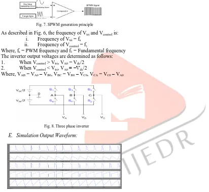
Fig. 7. SPWM generation principle
Fig. 8. Three phase inverter
Fig. 9. Output Current waveform of the Converter
Fig. 10. Output Voltage waveform of the Converter
C. SPWM Generation:
Amplitudes of the triangular wave (carrier) and sine wave (modulating) are compared to obtain PWM waveform. When the modulating signal is a sinusoid of amplitude Am, and the amplitude of the triangular carrier is Ac, the ratio m=Am/Ac is known as the modulation index. With a sufficiently high carrier frequency the high frequency components do not propagate significantly in the ac network (or load) due the presence of the inductive elements. However, a higher carrier frequency does result in a larger number of switching per cycle and hence in an increased power loss. Typically switching frequencies in the 2-15 kHz range are considered adequate for power systems applications.
D. Three Phase SPWM inverter:
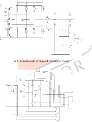
The circuit model of three-phase PWM inverter is shown in Fig.5. The waveforms of carrier wave signal (Vtri) and control signal (Vcontrol), inverter output line to neutral voltage (VA0, VB0, VC0), inverter output line to line voltages (VAB, VBC, VCA), respectively is shown in Fig. 6.
As described in Fig. 6, the frequency of Vtri and Vcontrol is: i. Frequency of Vtri = fs
ii. Frequency of Vcontrol = f1
Where, fs = PWM frequency and f1 = Fundamental frequency The inverter output voltages are determined as follows: 1. When Vcontrol > Vtri, VA0 = Vdc/2
2. When Vcontrol < Vtri, VA0 = −Vdc/2
Where, VAB = VA0 – VB0, VBC = VB0 – VC0, VCA = VC0 – VA0
E. Simulation Output Waveform:
IJEDR1604039 International Journal of Engineering Development and Research (www.ijedr.org) 247
Fig. 11. Output Voltage waveform of the Inverter
The above waveform shows the output voltage waveform across the capacitor C01, C02, C1 and the switch SW1
The above waveform shows the DC input voltage, and the line voltage (Eab,Ebc, and Eca) respectively.
III.
CONCLUSION
This project proposes a new high step-up DC–DC converter designed especially for regulating the dc interface between various microsources and a DC–AC 3Φ SPWM inverter to electricity grid. The converter achieves high step-up voltage gain with appropriate duty ratio and low voltage stress on the power switch. Additionally, the energy stored in the leakage inductor of the coupled inductor can be recycled to the output capacitor.The 3Φ SPWM inverter reduce the harmonics and achieves the high-voltage, high-power capability. Switching losses can be reduced by Soft switching techniques. To verify the performance of the proposed converter, a 280-W prototype sample is implemented with an input voltage range of 20–40 V and an output voltage of up to 400 V. The upmost efficiency of 93.3% is reached with high-line input; on the other hand, the full-load efficiency remains at 89.3% during low-line input.
The future work is to design a controller to drive the switching characteristics of the converter and inverter buy taking the reference value and measured value from the proposed system. Hence the system become closed-loop, which leads to increased stability.
R
EFERENCE[1] Y. W. Li and C. N. Kao, ―An accurate power control strategy for power electronics- interfaced distributed generation units operating in a low voltage multibus microgrid,‖ IEEE Trans. Power Electron., vol. 24, no. 12, pp. 2977–2988, Dec. 2009. [2] B. Axelrod, Y. Berkovich, and A. Ioinovici, ―Switched-capacitor/ switched-inductor structures for getting transformer less hybrid DC–DC PWM converters,‖ IEEE Trans. Circuits Syst. I, Reg. Papers, vol. 55, no. 2, pp. 687–696, Mar. 2008.
[3] F. L. Luo, ―Switched-capacitor zed DC/DC converters,‖ in Proc. IEEE Conf. Ind. Electron. Appl. (ICIEA), 2009, pp. 1074– 1079.
[4] R. J. Wai, C. Y. Lin, R. Y. Duan, and Y. R. Chang, ―High-efficiency DC-DC converter with high voltage gain and reduced switch stress,‖ IEEE Trans. Ind. Electron., vol. 5, no. 14, pp. 354–364, Feb. 2007.
[5] L. S. Yang, T. J. Liang, and J. F. Chen, ―Transformerless DC–DC converters with high step-up voltage gain,‖ IEEE Trans. Ind. Electron., vol. 56, no. 8, pp. 3144–3152, Aug. 2009.
[6] F. Zhang and Y. Yan, ―Novel forward-flyback hybrid bidirectional DC–DC converter,‖ IEEE Trans. Ind. Electron., vol. 56, no. 5, pp. 1578–1584, May 2009.
[7] K. C. Tseng and T. J. Liang, ―Novel high-efficiency step-up converter,‖ Proc. IEE Electric Power Appl., vol. 151, no. 2, pp. 182–190, Mar. 2004.
[8] S. K. Changchien, T. J. Liang, J. F. Chen, and L. S. Yang, ―Novel high step-up DC–DC converter for fuel cell energy conversion system,‖ IEEE Trans. Ind. Electron., vol. 57, no. 6, pp. 2007–2017, Jun. 2010.
[9] R. J.Wai and R. Y. Duan, ―High step-up converter with coupled-inductor,‖ IEEE Trans. Power Electron., vol. 20, no. 5, pp. 1025–1035, Sep. 2005.