ISSN(Online): 2320-9801 ISSN (Print): 2320-9798
I
nternational
J
ournal of
I
nnovative
R
esearch in
C
omputer
and
C
ommunication
E
ngineering
(An ISO 3297: 2007 Certified Organization)
Vol. 4, Issue 2, February 2016
Effects of an EBG Structure on Microstrip
Patch Antenna for LTE Mobile
Communication Systems
Balaji B.Wattamwar1, Prakash S. Andhare2
Associate Professor, Dept. of E & TC Engineering, MIT (T), Aurangabad, Maharashtra, India1
PG Student (Communication Engineering), Dept. of E & TC Engineering, MIT, Aurangabad, Maharashtra, India2
ABSTRACT: Long Term Evolution (LTE) to achieve very high data rates in both the uplink and downlink channels. Such antenna systems are required to fit within the hand-held (mobile) terminal which occupies a small size (typically not more than 60*100 mm2). Utilization of electromagnetic band-gap (EBG) structures is becoming attractive in the electromagnetic and antenna community. In this paper, the effects of a two-dimensional electromagnetic bandgap (EBG) Structures on the performance of microstrip patch antenna arrays are investigated using the HFSS.
Microstrip patch antennas became very popular because of planer profile, ease of analysis and fabrication, compatibility with integrated circuit technology & their attractive radiation characteristics. To improve surface wave losses uses Electro Magnetic Band Gap structures, for improving efficiency & bandwidth do proper impedance matching. This paper represents the design of Electromagnetic Band gap (EBG) structure having fractal shape and its effect on antenna performance. The aim of this paper is to design, simulate and fabricate the new EBG structure operating at 2.4GHz frequency and to study the performance of the rectangular microstrip antenna in terms of the bandwidth and VSWR with and without EBG structure which are characterized in terms of return loss and radiation pattern. The antenna has a measured Centre frequency of 2.4 GHz, bandwidth of 105 MHz and total size of 29.0 * 38.1 mm2.
KEYWORDS: Microstrip Antenna, Electromagnetic Band Gap (EBG), LTE, VSWR, Mutual Coupling, R. L. I. INTRODUCTION
Multiple-input-multiple-output (MIMO) transmission is one of the promising antenna technologies used for wireless communications. Through spatial multiplexing, MIMO achieves high capacities. The only limitation is that, the transmitting and receiving antennas should be placed at least half the wave length of the carrier signal in order to transmit or receive uncorrelated signals. Apart from that, each of transmit or receive antenna requires a separate circuit which means, higher the no of antennas used higher the cost. It is indisputable that antenna plays a significant part in communication system. Therefore, an increasingly number of technicians begin to do some research and development of antenna. However, with rapid development of the communication industry, the requirement of antenna will be achieved with high quality. Nowadays, there are different kinds of antennas in the market such as dipole antenna, microstrip patch antenna, loop antenna, meander-line antenna and so on [1].
ISSN(Online): 2320-9801 ISSN (Print): 2320-9798
I
nternational
J
ournal of
I
nnovative
R
esearch in
C
omputer
and
C
ommunication
E
ngineering
(An ISO 3297: 2007 Certified Organization)
Vol. 4, Issue 2, February 2016
The reason why microstrip antennas have become very popular is that they have several advantages compared to conventional microwave antennas; light weight, low volume, thin profile, low fabrication cost, easy integration with microwave integrated circuits, ease of installation, etc. are some of them. However, they do have some limitations such as narrow bandwidth, low gain, low power handling capability (~100W), large ohmic losses in feed structures. A lot of new techniques have evolved to minimize these limitations [6].
II. LITERATURESURVEY
Micro strip antenna is most common small sized antenna in which a metal patch is deposited on dielectric material. Micro strip patch antennas have been an attractive choice in mobile and radio wireless communication. Due to unique characteristics of an Electromagnetic bandgap (EBG) Structure, it enables it to be used in Radio frequency (RF) and microwave application which is considered to be among the significant breakthrough in the EBG technology nowadays. Many exciting phenomena appear when periodic structures interact with electromagnetic waves, which include band pass, band stop and also frequency band gap. Others include wave propagation, noise reduction for high speed electronic devices and mutual coupling effect reduction. Recently there is significant increase in utilizing EBG structures in antenna community [7].
Electromagnetic band gap structures sometimes called as photonic band gap materials are the artificially engineered objects that avert the propagation of electromagnetic waves in a specified band of frequency. These structures have interesting properties which cannot be seen in the natural materials such as they reflect incident plane wave’s in-phase rather than out of the phase [8].In this paper, the rectangular microstrip patch antenna has a new fractal electromagnetic band-gap (EBG) structure. The patch antenna is fed by a driven terminal and is integrated within a fractal electromagnetic band-gap structure, on same substrate to raise the antenna gain and bandwidth. The fractal electromagnetic band-gap structure applied is a periodic structure with similar periods[9].
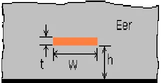
In its most basic form, a Microstrip patch antenna consists of a radiating patch on one side of a dielectric substrate which has a ground plane on the other side as shown in Figure 1. The patch is generally made of conducting material such as copper or gold and can take any possible shape. The radiating patch and the feed lines are usually photo etched on the dielectric substrate. In order to simplify analysis and performance prediction, the patch is generally square, rectangular, circular, triangular, and elliptical or some other common shape. For a rectangular patch, the length L of the
patch is usually 0.3333λ0 <L< 0.5 λ0, where λ0 is the free-space wavelength. The patch is selected to be very thin such that, t « λ0 (where‘t’is the patch thickness). The height h of the dielectric substrate is usually 0.003 λ0 <=h<=0.5 λ0. The dielectric constant of the substrate εris typically in the range 2.2 <= εr<= 12[10].
Fig.1 Structure of a Rectangle Microstip Patch Antenna
ISSN(Online): 2320-9801 ISSN (Print): 2320-9798
I
nternational
J
ournal of
I
nnovative
R
esearch in
C
omputer
and
C
ommunication
E
ngineering
(An ISO 3297: 2007 Certified Organization)
Vol. 4, Issue 2, February 2016
antenna size [11].
The typical electric field lines for a microstrip line are non-homogenous lines of two dielectrics viz. substrate and air. Most of the electric field lines reside in the substrate and parts of some lines exist in air shown in fig 2. As L/H>>1 and
εr >> 1, the electric field lines concentrate mostly in the substrate. Fringing in this case makes the microstrip line look
wider electrically compared to its physical dimensions. Since some of the waves travel in the substrate and some in air,
an effective dielectric constant εe is introduced to account for fringing and wave propagation in the line.The effective
dielectric constant is defined as the dielectric constant of the uniform dielectric material such that, the microstrip line with its original dimensions and height above the ground plane, embedded in this dielectric material, has identical electrical characteristics as the actual line, with air above the substrate.
Fig. 2 Effective dielectric constant geometry.
Typically, (εr>> 1), the value of εewill be closer to the value of the actual dielectric constant εr of the substrate. The
effective dielectric constant is also function of frequency. As the frequency of operation increases, most of the electric field lines concentrate in the substrate. Therefore, the microstrip line behaves more like a homogenous line of one dielectric (onlysubstrate), and the effective dielectric constant approaches the value of the dielectric constant of the substrate. The values of effective dielectric constant at low frequencies are referred to as the static values. For, W/h > 1,
W
h
r r e/
12
1
1
2
1
2
1
eq. (1)Because of the fringing effects, electrically the patch of the microstrip antenna looks greater than its physical dimensions as shown in fig. 3. For the principal E-plane (xy-plane), the electrical dimensions of the patch along its length have to be extended by a distance ∆L, which is function of the effective dielectric constant εe and the
width-to-height ratio (W/h). An approximate relation for normalized extension of the length is[12].
8
.
0
258
.
0
264
.
0
3
.
0
412
.
0
h
W
h
W
h
L
e e
eq. (2)Since the electrical length of the patch has been extended by ∆L on each side, the effective length of the patch is now
L
L
L
eff
2
eq. (3)∆L L ∆L
(a) Top view (b) Side view
ISSN(Online): 2320-9801 ISSN (Print): 2320-9798
I
nternational
J
ournal of
I
nnovative
R
esearch in
C
omputer
and
C
ommunication
E
ngineering
(An ISO 3297: 2007 Certified Organization)
Vol. 4, Issue 2, February 2016
In this work, we design and fabricate a single microstrip antenna on a effect EBG structure with a center frequency around 2.412 GHz, bandwidth of at least 105 MHz and total size of an antenna 29.0 X 38.1 mm. This paper presents an overview design microstrip patch antennas in the ISM band by providing a good initial geometrical configuration of the antenna. This article has-been divided into four sections. Section I describes introduction. Section II describes in detail of the literature survey on microstrip patch antenna structure and design. Section III describes in detail band gap characterization of the EBG structure. Section IV describes in detail modelling of the microstrip patch antenna with effect EBG structure. The results obtained from our proposed antenna are listed and discussed in Section V. Finally concluding remarks are presented in Section VI.
III.BANDGAPCHARACTERIZATIONOFTHEEBGSTRUCTURE
This technology manipulates the substrate in such a way that surface waves are completely forbidden from forming, resulting in improvements in antenna efficiency and bandwidth, while reducing side lobes and electromagnetic interference levels. These substrates contain so called Photonic Crystals. Also known as electromagnetic band-gap (EBG) structures and electromagnetic band-gap materials (EBMs), are a class of periodic metallic, dielectric, or composite structures that exhibit a forbidden band, or band gap, of frequencies in which waves incident at various directions destructively interfere and thus are unable to propagate. The first photonic-crystal structure conceptualized and manufactured was in 1991 by Yablonovitch, then at Bell Communications Research in New Jersey. If the periodicity in an EBG structure is perturbed by either removing or adding a material with a different dielectric constant, size, or shape, a “defect” state is created in the forbidden gap, where an electromagnetic mode is allowed, and localization of the energy occurs. This paper focuses the effect of two element microstrip patch antennas array on a uniform substrate and EBG structures. A mushroom-like EBG structure was compared to other EBG structures such as holes, this structure has a winning feature of compactness, which is important in communication antenna applications such as filters in microstrip lines, as high-power microwave components. Surface wave are excited on microstrip
antenna when the substrate єr > 1. Besides end fire radiation, surface wave give rise to coupling between various
elements of an array. Surface wave are launched into the substrate.
Fig. 4 Formation of Surface wavesFig.5 Fundamental Structure of an EBG
ISSN(Online): 2320-9801 ISSN (Print): 2320-9798
I
nternational
J
ournal of
I
nnovative
R
esearch in
C
omputer
and
C
ommunication
E
ngineering
(An ISO 3297: 2007 Certified Organization)
Vol. 4, Issue 2, February 2016
distinct stop band for surface-wave propagation. The operation mechanism of this EBG structure can be explained by an LC filter array. For an EBG structure with patch width W, gap width g, substrate thickness h and dielectric constant
εr, the values of the inductor L and the capacitor C are determined by the following formula [13][14].
= ˳ℎ eq. (4)
L = ˳( ℰ˳)cosℎ( )eq. (5)
μ0is the permeability of free space and ε0 is the permittivity of free space. Reference also predicts the frequency band
gap as
w =
√ eq. (6)
BW =∆ = √( )eq. (7) where η is the free space impedance which is 120π.
IV.MODELLINGOFTHEEBGMICROSTRIPANTENNA
Recently, considerable research effort in the electromagnetic band gap (EBG) structure for antenna application to suppress the surface wave losses and improve the radiation performance of the antenna. When source signal is applied at metal ground plane & patch, the EM waves will be radiated. The radiation will not be perfect as there are some losses due to dielectric material. We have to minimize these losses. To minimize these losses we will insert EBG structures with Micro strip Patch Antenna.
EBG stands for Electromagnetic Band Gap Substrate. Electromagnetic band gap structures are defined as artificial periodic or sometimes non-periodic objects or say that dielectric materials and metallic conductors that prevent the propagation of electromagnetic waves in a specified band of frequency for all incident angles and all polarization states. At present time, there is a need of smaller and broad bandwidth antennas. This can be achieved by fabrication of antenna on thick piece of high permittivity substrate. The main disadvantage is that, the unwanted substrate modes begin to form and propagate towards the edges of the substrate, which have a deadly effect on the antenna radiation pattern.
EBG can be categorized into three groups according to their geometric configuration: 1. Three-dimensional volumetric structures.
2. Two-dimensional planar surfaces. 3. One-dimensional transmission lines.
ISSN(Online): 2320-9801 ISSN (Print): 2320-9798
I
nternational
J
ournal of
I
nnovative
R
esearch in
C
omputer
and
C
ommunication
E
ngineering
(An ISO 3297: 2007 Certified Organization)
Vol. 4, Issue 2, February 2016
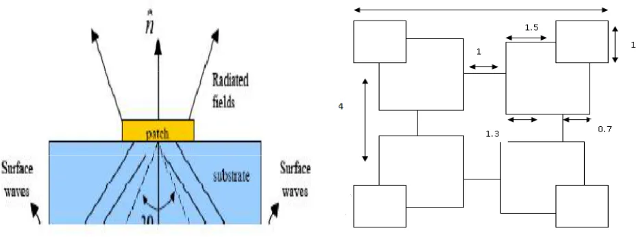
Fig.6. Geometry of the microstrip patch antennaTable I: Simulated results fordiff. width of the microstrip feed line. V. SIMULATIONRESULTS
Figure 7 shows the top views of the fabricated single microstrip patch antenna structure. The radius of the sphere inclosing this antenna is 1.45. Figure 8 shows the measured and simulated reflection coefficients. An HP 8514BNetwork Analyzer was used to conduct this measurement. The correlation between the two is very well observed. The simulated fc was 2.41 GHz, while the measured one was 2.40 GHz. The simulated -10 dB bandwidth was
105 MHz while the measured one was 95 MHz. This shows a good match between the two, although some discrepancy is expected due to the presence of the GND plane. The MLA total size is 29.0 X 38.1 mm.
Fig.7 Photo of the fabricated Microstrip AntennaFig.8 Simulated R. L. for proposed Microstrip Antenna This section presents the simulated results of modified microstrip patch antenna. HFSS has been used to simulate the antenna for several performance parameters such as impedance bandwidth, radiation patterns and VSWR. The parametric study of the antennas reveals the band behavior. The antenna is designed to operate on 2.41 GHz ISM band. Fig. 8 illustrates the S11 of microstrip patch antenna; where it shows a return loss of -25.1 dB for the operation on 2.41 GHz. The impedance bandwidth calculated at -10 dB scale for this band is 105 MHz. Figure 9 shows the simulated and measured VSWR for proposed microstrip patch antenna. In small antennas, the ground plane plays a major part in radiation. The current distribution on the ground plane and its effect on the resonant frequencies were also observed during simulation. The measured radiation patterns for the single element microstrip patch antenna are shown in figure 10.
Fr (GHz)
Width (mm)
Length (mm)
R.L.
(dB) VSWR
Gain (dB)
Directi vity
2.4121 3 9
-25.03 1.27 5.5 5
2.4121 4 9
-19.94 1.33 5.5 5
2.4121 5 9
-17.39 1.56 5.5 5
2.4121 6 9
ISSN(Online): 2320-9801 ISSN (Print): 2320-9798
I
nternational
J
ournal of
I
nnovative
R
esearch in
C
omputer
and
C
ommunication
E
ngineering
(An ISO 3297: 2007 Certified Organization)
Vol. 4, Issue 2, February 2016
Fig.9 Simulated VSWR for proposed Microstrip Antenna Fig.10 Radiation Pattern of Proposed Microstrip Antenna VI.CONCLUSIONANDFUTUREWORK
A compact electromagnetic Band Gap (EBG) design and fabrication that is based on the microstrip patch antenna is presented. The antenna is intended for the use in the 2.4-2.7 GHz of the LTE mobile communication applications. Simulation and measurement results are compared. The single antenna has a measured center frequency of 2.41 GHz, bandwidth of 105 MHz, Return loss -25.1 is obtained and total size of antenna is 29.0 X 38.1 mm.
The Microstrip Patch Antenna with EBG is simulated by using HFSS, fabricated and there results are compared.The antenna gain and directivity are also increased while the back lobes are reduced. The gain is increased from 3.48dB to 5.55dB for both types of EBG structures. Using the EBGs around the patch antenna in the same plane, the surface waves are suppressed effectively. Therefore, the performances of the antenna are improved greatly.The fractal EBG structure has been proposed. A comparative study of simple rectangular microstrip antenna without and with EBG had been demonstrated. The bandwidths, gain of the antenna get improved. This antenna can be used in many applications. Future work for the proposed control methodology is that it can be used with various antenna designs to obtain different possible results in an easy, fast, and low-cost manner.
Better Antennas can be designed and implemented by following tasks to be done in future to make the designed antenna more flexible while using in wireless applications.
The VSWR of the antenna can be improved by using of thermo compression bonding or spot soldering.
The bandwidth of the antenna can be improved by mentioning the chu limit.
The input impedance of the antenna can be improved by slightly reducing the inset distance.
The Efficiency of the antenna can be increased by increasing the no. of turns.
REFERENCES
1. Chandana K. K. Jayasooriya, Hyuck M. Kwon and Seok Bae, Yang-Ki Hong,“Miniaturized Circular Antennas for MIMO Communication
Systems – Pattern Diversity pp.331-334 2010 International ITG. Workshop on Smart Antennas (WSA 2010).
2. V. K. Garg, Wireless Communications and Networking, Elsevier-Morgan Kaufmann, 2007.
a. Larmo, et. al., “The LTE Link-Layer Design,” IEEE Commun. Mag., Vol. 47, No. 4, pp. 52-59, April 2009.
3. 3 GPPTS 36.101,V8.3.0, “EUTRA User Equipment Radio Transmissionand Reception,” September 2008.
4. J. D. Kraus, R. J. Marhefka, Antennae for all applications, Tata McGraw Hill, 3rd Edition.
a. A. Balanis, Antenna Theory: Analysis and Design. New York: Wiley,Second ed., 1997.
5. Muhammad Abdulhamid1, M. K. A. Rahim, Umar Musa, “Electromagnetic Bandgap Structure for Antenna Design”, IOSR Journal of
Electronics and Communication Engineering (IOSR-JECE) e-ISSN: 2278-2834,p- ISSN: 2278-8735.Volume 10, Issue 6, Ver. I (Nov - Dec .2015), PP 2527
6. Ajay kumar,DwejendraArya,D.KSrivastava,"Band Width of Microstrip Antenna Improved by using Mushroom type EBG Structure",IEEE
ISSN(Online): 2320-9801 ISSN (Print): 2320-9798
I
nternational
J
ournal of
I
nnovative
R
esearch in
C
omputer
and
C
ommunication
E
ngineering
(An ISO 3297: 2007 Certified Organization)
Vol. 4, Issue 2, February 2016
7. F. Yang, Y. Rahmat-Samii, “Microstrip Antennas integrated with electromagnetic band-gap structure: a low mutual coupling design for array
application,” IEEE Trans. Antennas and Propagation, Vol. 51, Oct. 2003.
8. Yen-Liang Kuo. Tzung-Wern Chiou. Kin-Lu Wong. A dual-band rectangular microstrip antenna using a novel photonic band gap ground plane
of unequal orthogonal periods. Microwave and optical technology IERS. Vol. 30, No.4, Aug. 2001. pp. 280-283.
9. George Splitt, Marat Davidovitz, Guidelines for design of electro-magnetically Coupled microstrip patch Antennae on two layer substrates. IEEE transactions on Antennae and Propagation. Vol. 38,. No. 7 July 1990.Pp. 1136 – 1140
10. P. C. Sharma, K. C. Gupta. "Analysis and optimum design of single feed circularly polarized microstrip antenna" IEEE Transaction on Antenna
& Propagation. Vol. AP-31. No.6 November 1983.
11. H. F. Shaban, H. A. Elmikaty, and A. A. Shaalan, “Study The Effects Of Electromagnetic Band-Gap (EBG) Substrate On Two Patches
Microstrip Antenna”, Progress In Electromagnetics Research B, Vol. 10, 55–74, 2008.
12. Xu, H.J., Y. H. Zhang, and Y. Fan, “Analysis of the connection between K connector and microstrip with electromagnetic bandgap (EBC) structures,” Progress In ElectromagneticResearch, PIER 73, 239–247, 2007.
BIOGRAPHY
Balaji B. Wattamwar is former I/c Principal at SSCOE, Pardari, Aurangabad. He is an Associate Professor in the Electronics & Telecommunication Department, MIT, Aurangabad.He received Master of Technology (M Tech) degreefrom JNTU, Hyderabad, AP, India. His research interests are Microwave & antenna, VLSI & Embedded system design.