ISSN(Online): 2320-9801
ISSN (Print): 2320-9798
I
nternational
J
ournal of
I
nnovative
R
esearch in
C
omputer
and
C
ommunication
E
ngineering
(An ISO 3297: 2007 Certified Organization)
Vol. 4, Issue 2, February 2016
Skew Reduction with Buffer Insertion for
Synchronous System
*R. Muthu Selvi1,J. Thilagavathy2, G. Ewance Lidiya3
PG Student, Department of Electronics, Dr.Sivanthi Aditanar College of Engineering, Tamil Nadu, India1*
Asst. Professor, Department of Electronics, Dr.Sivanthi Aditanar College of Engineering, Tamil Nadu, India2
Asst. Professor, Department of Electronics, Dr.Sivanthi Aditanar College of Engineering, Tamil Nadu, India3
ABSTRACT: The design which utilizes different power modes will leads to reduction in energy consumption. In a multi-power-mode design, the range of the supply voltage becomes wide. Thus large clock skew may occur among different power domains in the system. Difference in arrival time of clock signal across the chip is called clock skew. Clock skew can be minimized by clock tree optimization which inserts Buffer chain to balance clock skew among modules. The novel architecture is composed of two serially connected sub-buffers which can operate at low and high voltage level respectively. In the front sub-buffer, the low voltage level is used for coarse-grained reduction of clock skew. In the back sub-buffer, the high voltage level is used for fine-grained reduction of clock skew.
KEY WORDS - Buffer, clock signal, Clock skew, Level Up Shifter, Sequential circuit.
I. INTRODUCTION
One of the main aspects of digital VLSI system is the design of sequential circuits. The general structure of sequential circuit is shown in Fig. 1. The primary output from the combinational logic is stored in the D flip- flop (FF) and the primary input is given as the input to combinational logic. The outputs of sequential circuits can be generated which are not only dependent on the present input conditions, but it also depend on the past inputs history. These input histories are provided with the help of feedback that is connected from the output to the input. The general structure of sequential circuit contains memory elements and the combinational circuit as the feedback path.
Clock skew is a phenomenon in synchronous circuits in which the clock signal that is sent from the clock circuit arrives at different components at various times. Clock skew can be sometimes called as timing skew. Clock skew can be caused by different things, such as wire-interconnect length, variations in temperature, variation in intermediate devices, coupling that caused by capacitor, imperfections in material, and differences in input capacitance on the clock inputs of devices using the clock.
Fig. 1. The general structure of sequential circuit
ISSN(Online): 2320-9801
ISSN (Print): 2320-9798
I
nternational
J
ournal of
I
nnovative
R
esearch in
C
omputer
and
C
ommunication
E
ngineering
(An ISO 3297: 2007 Certified Organization)
Vol. 4, Issue 2, February 2016
receiving register gets the clock tick faster than the sending register. Zero clocks skew refers to the arrival of the clock tick simultaneously at transmitting and receiving register.
Two different violations can cause by clock skew. First problem is occurred when the clock signal propagates slower than the path from one to another register - allowing information to go through two registers in the same clock edge. This is known as a hold violation because the record is not held enough at the flip-flop to be suitably clocked through. Second problem is caused when the destination flip-flop gets the clock tick former than the source flip-flop - the information signals have that much small time to arrive at the destination flip-flop before the next clock signal. If it fails to do like this, then a setup violation can occur, because the new data was not stable before the next clock arrived.
II. RELATED WORK
Adjustable Delay Buffer (ADB) is used whose delays can be adjusted to reduce clock skew as discussed in [1]. The conventional buffer architecture [2] can be operated at high voltage only. The conventional buffer architecture is used to remove the clock skew among different power domains. In synchronous circuit designs, clock skew is difficult to minimize because a single physical layout of a clock tree must satisfy multiple constraints in a complicated power mode environment where certain modules may operate with different voltages. Adjustable Delay Buffer (ADB) is used whose delays can be tuned or adjusted to minimize clock skew under different power modes as described in [3]. A tuneable clock tree structure is proposed by adopting the adjustable delay buffers (ADBs) in [4]. The ADBs can be used to produce additional delays and hence the clock latencies and skew become tuneable in a clock tree. Importing a buffered clock tree, the ADBs with delay value assignments are inserted to reduce clock skew in MDSV designs. A variation-aware ULV clock network design methodology is introduced in [5]. The process of adding more buffers in the middle of a capacitive interconnect does not help reduce the delay. However, the results showed that a buffered interconnects are advantageous to improve slew under comparable power consumption. The ultra low voltage level power analysis method is explained in [7].
III. DESIGN METHODOLOGY
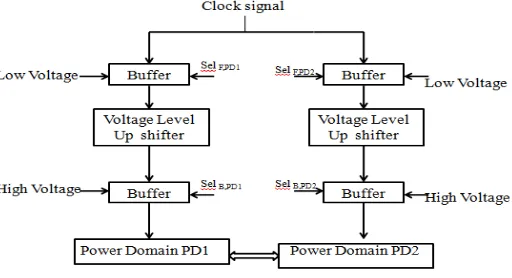
The use of multiple power modes can reduces the power consumption but the reduction of clock skew turns to be very difficult in several power modes. In general, as the supply voltage is reduced to the ultralow voltage, the scope of the supply voltage becomes wide. A Power Domain (PD) can be defined as some set of modules that are always at the similar voltage level. Since those set of modules are in same voltage, consumption of power will be over headed in Power Domain.
Fig. 2. Two voltage stage PMAB clock tree
ISSN(Online): 2320-9801
ISSN (Print): 2320-9798
I
nternational
J
ournal of
I
nnovative
R
esearch in
C
omputer
and
C
ommunication
E
ngineering
(An ISO 3297: 2007 Certified Organization)
Vol. 4, Issue 2, February 2016
eliminate the clock skew. The large amount of the clock skew can be removed in the first stage. In Fig. 2, SELF,PD is the selection signal to the multiplexer which is in front sub-buffer, similarly SELB,PD is the selection signal to the multiplexer in the back sub-buffer, and the values of SELF,PD and SELB,PD are generated according to the corresponding power domain PD. Design process consists of two phases such as buffer and Voltage Level Up Shifter.
A. Design process of buffer
The novel buffers have to be inserted into a clock tree to balance the clock skew among various modules. This is a super buffer with selection capability. The delays of a buffer can be adjusted.
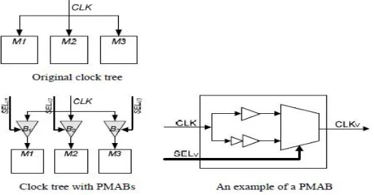
The variation among the terms voltage mode as well as power mode has to be identified for design process of buffer. Voltage mode refers to various operating voltages of a module, while the power mode refers to various configurations of the operating voltages for a module. For instance there may be five power modes for standard design: Active 1, Full Speed, Active 2, Inactive and Suspend. All modules such as MPU, DSP may have only two voltages 1.2V and 1.0V respectively. The design buffer with easier example is depicted in Fig. 3.
Fig. 3. An example of PMAB and clock tree with PMAB
Steps for designing a PMAB
First step is to record the global clock latency called Lglobal. Then record the latency of all modules LPDi.
Second step is to calculate the delay for each module. Integer Linear Programming approach is used to compute the number of buffers in each buffer chain.
Buffer can be designed as a “tunable” delay element. The select signal can be a type of mode. It is used to select a set of the equivalent delays.
The buffer can be designed using a MUX with the select signal as shown in Fig. 3.
After insertion of buffer, determine the clock skew. Now the value of clock skew will be equal to zero.
B. Design process of voltage Level Up Shifter
ISSN(Online): 2320-9801
ISSN (Print): 2320-9798
I
nternational
J
ournal of
I
nnovative
R
esearch in
C
omputer
and
C
ommunication
E
ngineering
(An ISO 3297: 2007 Certified Organization)
Vol. 4, Issue 2, February 2016
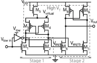
Fig. 4. Circuit level schematic of voltage Level Up Shifter
Two voltage buffer architectures have fixed the voltage level, so DVS controller is not required. But the front sub-buffer is at the low voltage and the back sub-sub-buffer is at the high voltage. Thus there is a need to convert from low to high voltage level. Therefore, a voltage level-up shifter has to be inserted into the path from the front sub buffer to the back sub buffer. Level up Shifter concepts are explained in [6] to convert from low voltage level to high voltage level. Energy efficient level converter is shown in Fig. 4. Thus clock signal is made to reach different power domain at the same time in order to reduce the clock skew.
IV. RESULTS AND DISCUSSIONS
The design is simulated using Tanner EDA and Altera Quatrus – II. The clock skews of sequential circuits are calculated using Time Quest Analyzer in Altera Quatrus – II. The schematic of voltage Level Up Shifter is drawn using Tanner EDA tool and the corresponding output is obtained. The buffer is designed by using Xilinx 14.5 version tool. The input and the output waveform generated during the simulation are given below. Detailed experimental results for bench mark circuits are described in [8].
A. SIMULATION RESULT FOR BUFFER
The verilog code for PMAB is synthesized in Xilinx 14.5 version tool. The modified clock signal is delayed with respect to the value of selection line. The RTL schematic of PMAB is shown in Fig. 5.
Fig. 5. RTL schematic of PMAB
ISSN(Online): 2320-9801
ISSN (Print): 2320-9798
I
nternational
J
ournal of
I
nnovative
R
esearch in
C
omputer
and
C
ommunication
E
ngineering
(An ISO 3297: 2007 Certified Organization)
Vol. 4, Issue 2, February 2016
Fig. 6. Output waveform of PMAB
The output waveform of PMAB is shown in Fig. 6. The clock signal is delayed by 3 buffer elements in one buffer chain and another buffer chain has only one buffer. The delay of buffer is assigned to 10 ns.
B. SIMULATION RESULTS FOR VOLTAGE LEVEL UP SHIFTER
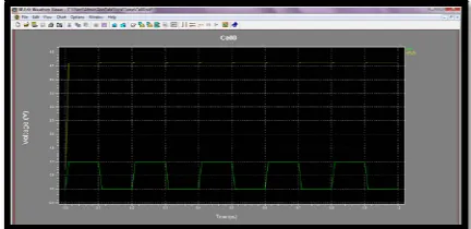
The design of voltage Level Up Shifter is done by using both Tanner EDA tool and Xilinx 14.5 version tool. The schematic of voltage Level Up Shifter is drawn in Tanner EDA tool and corresponding output is obtained. The schematic is shown in Fig. 7.
Fig. 7. Schematic of voltage LUS
The input voltage is set as 1V and output is increased to 4.7V. The output waveform is shown in Fig. 8. Thus Level Up Shifter is used to convert low voltage level to higher voltage level.
ISSN(Online): 2320-9801
ISSN (Print): 2320-9798
I
nternational
J
ournal of
I
nnovative
R
esearch in
C
omputer
and
C
ommunication
E
ngineering
(An ISO 3297: 2007 Certified Organization)
Vol. 4, Issue 2, February 2016
C. SIMULATION RESULTS FOR SEQUENTIAL CIRCUITS
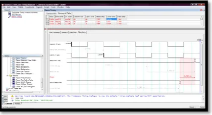
The calculation of clock skew is first calculated in 64 – bit shift register which has input of 64 - bits which consists of 64 D – FF. The technology map viewer (post mapping) of 64 – bit shift register is shown in Fig. 9.
Fig. 9. Technology mapping (Post mapping) for 64 – bit shift register
The clock skew value and waveform of clock pulse for 64 – bit shift register is shown in Fig. 10.
Fig. 10. Time Quest Analyzer for 64 – bit shift register
The waveform in Fig. 10 shows that clock skew is occurred between D-FF 23 and D-FF 24.
Clock skew = Launch clock delay – Latch clock delay
= 2.357 – 2.348 Clock skew = 0.009
The data delay is noted as 1.491 ns.
ISSN(Online): 2320-9801
ISSN (Print): 2320-9798
I
nternational
J
ournal of
I
nnovative
R
esearch in
C
omputer
and
C
ommunication
E
ngineering
(An ISO 3297: 2007 Certified Organization)
Vol. 4, Issue 2, February 2016
Fig. 11. Time Quest Analyzer for 64 – bit shift register after insertion of buffer
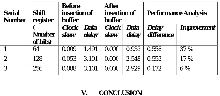
Similarly the same process is carried for several shift register by varying number of bits such as 128 bits shift register and 256 bit shift register. The details are shown in TABLE 1
Table I Performance analysis of sequential circuits
Serial Number Shift register ( Number of bits) Before insertion of buffer After insertion of buffer Performance Analysis Clock skew Data delay Clock skew Data delay Delay difference Improvement
1 64 0.009 1.491 0.000 0.933 0.558 37 %
2 128 0.053 3.101 0.000 2.548 0.553 17 % 3 256 0.088 3.101 0.000 2.929 0.172 6 %
V. CONCLUSION
The clock skews of sequential circuits are calculated using Time Quest Analyzer in Altera Quatrus – II. The schematic of voltage Level Up Shifter is drawn using Tanner EDA tool and the corresponding output is obtained. The buffer is designed by using Xilinx 14.5 version tool. Buffers have to be inserted in the clock path from clock generator and Power Domain to balance the clock skew among all the modules. By insertion of buffer (delay element) at appropriate positions, the clock skew is fully removed. Experimental results show that zero clock skew with reduced data delay is achieved.
VI. ACKNOWLEGMENT
ISSN(Online): 2320-9801
ISSN (Print): 2320-9798
I
nternational
J
ournal of
I
nnovative
R
esearch in
C
omputer
and
C
ommunication
E
ngineering
(An ISO 3297: 2007 Certified Organization)
Vol. 4, Issue 2, February 2016
REFERENCES
[1] Tu W.-P. Chou C.-H. Huang S.-H. Chang S.-C. Nieh Y.-T. and Chou C.-Y. (2013), “Low-power timing closure methodology for ultra-low voltage designs”, in Proc. IEEE Int. Conf. Computer.-Aided Design (ICCAD), San Jose, CA, USA, Nov, pp. 697–704.
[2] Wooters S. N, Calhoun B. H. and Blalock T. N. (2010), “An energy-efficient sub threshold level converter in 130-nm CMOS”, IEEE Trans. Circuits Syst. II, Exp. Briefs, vol. 57, no. 4, pp. 290–294, April.
[3] Y.-S. Su, W.-K. Hon, C.-C. Yang, S.-C. Chang, and. Y.-J. Chang, “Value assignment of adjustable delay buffers for clock skew minimization in multi-voltage mode designs,” in Proc. IEEE Int. Conf. Comput.-Aided Design (ICCAD), San Jose, CA, USA, Nov. 2009, pp. 535–538. [4] K.-Y. Lin, H.-T. Lin, and T.-Y. Ho, “An efficient algorithm of adjustable delay buffer insertion for clock skew minimization in multiple
dynamic supply voltage designs,” in Proc. 16th IEEE Asia South Pacific Design Autom. Conf. (ASP-DAC), Yokohama, Japan, Jan. 2011, pp. 825–830.
[5] X. Zhao, J. R. Tolbert, C. Liu, S. Mukhopadhyay, and S. K. Lim, “Variation-aware clock network design methodology for ultra-low voltage (ULV) circuits,” in Proc. IEEE Int. Symp. Low Power Electron. Design (ISLPED), Fukuoka, Japan, Aug. 2011, pp. 9–14.
[6] Koo K.-H. Seo J.-H. Ko M.-L. and Kim J.-W. (2005), “A new level-up shifter for high speed and wide range interface in ultra deep sub-micron”, in Proc. ISCAS, vol. 2, pp. 1063–1065.
[7] Ampadu P. (2006), ‘Ultra-low voltage VLSI : are we there yet?’, in Proc. Of ISCAS, pp. 21-24.
[8] Chou C.H et.al. “Detailed experimental results”, Chung Yuvan Christian Univ., Taoyuan, Taiwan, Apr.2015.
BIOGRAPHY
R. Muthu Selvi is a PG student of VLSI Design in Electronics Department, Dr. Sivanthi Aditanar College of Engineering College under Anna University, Chennai. She received her Bachelor of Engineering degree in 2014 from Kalasalingam University.
J. Thilagavathy is currently working as Assistant Professor in Electronics department, Dr. Sivanthi Aditanar College of Engineering. She received her Bachelor of Engineering from Dr. Sivanthi Aditanar College of Engineering and Master of Engineering from Raja Engineering College, Madurai.