CHARACTERIZATION TECHNIQUES FOR LIQUID CRYSTAL MATERIALS AND ITS APPLICATION IN OPTOELECTRONICS DEVICES
Vishal Sharma1, Dr. Anil Kumar2
Department of Physics
1,2
OPJS University, Churu, Rajasthan (India)
Abstract
This research employs characterization techniques for liquid crystal materials and its application in optoelectronics devices. Two-dimensional (2D) nanocomposite materials with dynamically tunable liquid crystalline properties have as of late developed as a highly-encouraging class of novel, useful materials, opening new courses inside a wide assortment of potential applications from the deposition of highly uniform layers and heterostructures, to novel display technologies. Here, we will present the fundamental ideas that support this ongoing mechanical progress; give an outline of the engineered courses towards such 2D nanocomposite materials; and survey late advances in the application and appropriateness of these materials inside the fields of optoelectronics and photonics. Since the approach of graphene in 2004, there has been a blast in the examination of an extensive variety of molecularly thin (two-dimensional) materials.
1. OVERVIEW
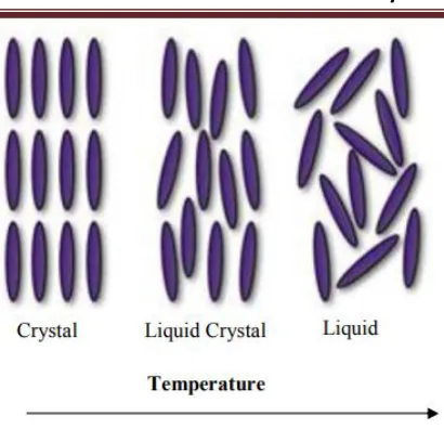
The liquid crystal phase is a phase of issue that exists for an assortment of particles and materials, contingent upon their geometric and substance properties, with qualities middle to those of an ordinary crystalline strong and a liquid[1]. Liquid crystals (LCs) have discovered use in an assortment of applications as the years progressed. The liquid crystal phase was at first portrayed by Austrian botanist Friedrich Reinitzer in 1888 when taking a gander at the properties of cholesterol subsidiaries, albeit some credit likewise goes to Julius Planer, who announced comparable perceptions 27 years prior[2].
This new and unmistakable condition of issue was then recognized as the "liquid crystal phase" by Otto Lehmann in 1890 and
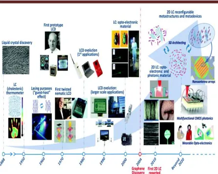
Figure 1Timeline of the History of Liquid Crystal Phase Applications, From Their Discovery to the Present Day
During the 1950s, the innovation of the primary cholesteric LC temperature pointers, and additionally advances in scientific metrology, tumor diagnostics, and non-ruinous material testing techniques drove another period in liquid crystal science. By 1962, liquid crystals were at that point discovering applications in best in class laser devices, in spite of the relative youth of laser science. Be that as it may, the most critical mechanical advancement came in 1965 with the improvement of the primary LC displays (LCDs). Like this, wound nematic LCDs (1969– 1971) propelled the field further[4].
Huge leaps forward in the advancement of liquid crystal technologies happened in the 1980– 1990s and kept on having a significant effect on everyday life: the scaling down of display technologies encouraged the improvement of compact PCs, cell phones and innumerable other innovations[5]. Since, the beginning of the new thousand years, LCs and as of late
found 2D material LCs have come into the request as optoelectronic and photonic materials. The likelihood of the presence of a liquid crystal phase stems basically from the geometric structure of the particles in the material, and also the practical groups exhibit in the atom.
In lyotropic liquid crystals, mesogens are scattered in a host dissolvable (regular water however other natural solvents can be utilized relying upon the atom). Lyotropic liquid crystals show a liquid crystal phase inside a specific scope of temperatures yet also require a centralization of the dynamic mesogens that falls inside a specific range. In the lyotropic phase, the ease of the material is prompted by the dissolvable particles as opposed to being characteristic for the mesogens themselves. The mesogens contain immiscible solvophilic and solvophobic parts isolated at contradicting 'finishes' or aspects of the particle, making them amphiphilic.
2. LIQUID CRYSTALS
Figure 2 Schematic illustrations of the crystalline solid, liquid crystal and isotropic liquid
LC materials are bounteous in nature as proteins, cell films and viruses. They are utilized as a part of the assembling of numerous electronic devices to be specific level LC display (LCD), plasma TV screens, guides, cell phones, individual advanced aides, organic lighting, solar cells devices, and so on. Because of this, there is an expanding interest for LC materials for different applications. The simple process capacity and great reasonableness make these organic materials extremely appealing towards numerous application perspectives. In addition to that the hydrogen bonded liquid crystals (HBLC) have earned research enthusiasm towards the different application aspectsin the most recent two decades.
3. TYPES OF THERMOTROPIC LIQUID CRYSTALS
Based on the positional and orientation orders of molecules, it is classified into two types
1. Orthogonal phase 2. Tilted phase.
These phases are further again sub-divided into many types. Mainly it is classified into
1. Nematic (N) phase 2. Cholesteric phase and 3. Smectic (Sm) phase. 4. This type of separation.
Further, thermotropic LC are classified according to their molecular shape and is alienated into
1. Calamitic LC 2. Discotic LC (DLC) 3. Polymeric LC
4. Banana shape of rod like, disc like and bend core molecules.
Nematic phase
N phase is the most vital phase in the LC. The name N landed from Greek word nema which implies string like structure. This term impels from string like topological structure which is seen in the Ns, and is formally called as disclinations. Ns are additionally called hedgehog topological imperfections.
Cholesteric Phase
4. SYNTHESIS AND CHARACTERIZATION TECHNIQUES
These days blend of high-quality materials with wanted properties is most extreme imperative in the consolidated test issue physical science research. A few physical, chemical and natural combination methods have been produced to upgrade the performance of nanomaterials displaying enhanced properties with the intent to have a little control over the particle measure appropriation and morphology. The required nanostructure can be blended in an assortment of shapes and sizes relying on their necessities, for example, single crystals, composite, undefined solids, thin films, thick films, polycrystalline powder, and so forth.
6. CHARACTERIZATION AND
TEXTURE OBSERVATIONS OF
CALAMITIC LIQUID CRYSTALLINE COMPOUNDS
Liquid crystalline conduct has been watched for the most part in two kinds of molecules: linear or bar like molecules that frame calamitic phases and circle like molecules that shape discotic phases. The structure of liquid crystalline phases is described by the game plan of the molecules, the compliance of the molecules, and the intermolecular collaborations. The transition between the different liquid crystal mesophases from crystalline to smectic to nematic happens at characterized temperatures which can be distinguished utilizing differential filtering calorimetry, while the nature and surface of the mesophase is typically investigated utilizing enraptured optical microscopy.
5. OPTOELECTRONICS
Liquid crystalline nanocomposites fusing 2D material particles demonstrate awesome guarantee for optoelectronic applications because of their field prompted tunability and upgraded usefulness originating from the plenty of properties displayed by the scope of exfoliative materials. For instance, scatterings of liquid crystalline graphene oxide have been appeared to experience electro-optical exchanging with low edge voltage necessities. By balancing out a suspension of diminished GO utilizing surfactants, they showed expanded time security and enhanced electro-optic properties with an initiated birefringence twice as vast at a similar field quality as that with an unreduced GO suspension.
5.1 Optoelectronic Property
5.2 Application and Prospectus
The self-assembling nature of liquid crystalline materials has prompted the utilization of graphene oxide scatterings for the arrangement of all around requested layers and piles of 2D materials. That graphite suddenly sheds into single-layer graphene in chlorosulfonic corrosive, and immediately frames liquid-crystalline phases at high concentrations. Straightforward, directing movies were delivered from the liquid crystalline scatterings. The readied scatterings were utilized to accomplish self-amassed layer-by-layer multifunctional 3D crossover structures involving SWNTs and GO with promising mechanical properties.
5.3 Types of Optoelectronics Devices with Applications
Optoelectronics is the communication between optics and electronics which includes the study, design and manufacture of a hardware device that converts electrical energy into light and light into energy through semiconductors. This device is made from solid crystalline materials which are lighter than metals and heavier than insulators. Optoelectronics device is basically an electronic device involving light. This device can be found in many optoelectronics applications like military services, telecommunications, automatic access control systems and medical equipment’s.
This academic field covers a wide range of devices including LEDs and elements, image pick up devices, information displays, optical communication systems, optical
storages and remote sensing systems, etc. Examples of optoelectronic devices include telecommunication laser, blue laser, optical fiber, LED traffic lights, photo diodes and solar cells. Majority of the optoelectronic devices (direct conversion between electrons and photons) are LEDs, laser diodes, photo diodes and solar cells. Optoelectronics are classified into different types such as:
Photodiode Solar Cells
Light Emitting Diodes Optical Fiber
Laser Diodes
Photo Diode
A photo diode is a semiconductor light sensor that creates a voltage or current when light falls on the intersection. It comprises of a functioning P-N intersection, which is worked backward inclination. At the point when a photon with a lot of vitality strikes the semiconductor, an electron or entire combine is made. The electrons diffuse to the intersection to frame an electric field. This electric field over the exhaustion zone is equivalent to a negative voltage over the unprejudiced diode. This strategy is otherwise called the internal photoelectric effect. This device can be utilized as a part of three modes: photovoltaic as a sun powered cell, forward one-sided as a LED and turn around one-sided as a photo identifier.
Solar Cells
over sun's energy into electricity. At the point when sunlight falls on a solar cell, it produces both a current and a voltage to deliver electric power. Sunlight, which is made out of photons, transmits from the sun.
Light-Emitting Diodes
Light-emitting diode is a P-N semiconductor diode in which the recombination of electrons and openings yields a photon. At the point when the diode is electrically one-sided the forward way, it emanates incongruous tight spectrum light. At the point when a voltage is connected to the leads of the LED, the electrons recombine with the gaps inside the device and discharge energy as photons. This effect is called as electroluminescence.
Optical Fiber
An optical fiber or optic fiber is a plastic and straightforward fiber made of plastic or glass. It is to some degree thicker than a human hair. It can work as a light pipe or waveguide to transmit light between the two finishes of the fiber. Optical filaments as a rule incorporate three concentric layers: a center, a cladding and a coat. The center, a light transmitting district of the fiber, is the focal segment of the fiber, which is made of silica. Cladding, the defensive layer around the center, is made of silica.
6. ELECTRONIC AND
OPTOELECTRONIC APPLICATIONS
Inorganic materials are favored for NLO applications over organic materials. The single crystals of unadulterated inorganic materials, for example, quartz, lithium
niobate (LINbO3), potassium dihydrogen
phosphate (KDP), potassium titanyl phosphate (KTP), and urea, show excellent NLO properties. These are the unadulterated inorganic materials utilized as a part of second harmonic generating devices, parametric oscillators, and so forth. A portion of the recognizable properties of inorganic host materials are huge mechanical quality, excellent thermal soundness, great transmittance, and high electro-optic coefficients and additionally high level of chemical inactivity.
wavering (OPO), optical emanation and electro-optical applications.
7. CONCLUSION
We displayed difficulties of existing 2D material process innovations, to be specific contaminations, reproducibility, and versatility. An assortment of 2D photonic devices that demonstrate additional functionalities contrasted with best in class mass devices was exhibited. A portion of the characteristic properties of graphene, for example, the nonappearance of an electronic band hole, transporter multiplication, and high bearer portability, propose applications as broadband and high-speed photodetectors, which have been demonstrated in a few occurrences. Even though the monoatomic idea of graphene presents a limitation in the absorbance, numerous promising solutions are being sought after.
New impetuses and critical advance in investigations of ring opening polymerization (ROP) and ring opening metathesis polymerization (ROMP) take into account much better characterized polymeric structures. Vital info can be relied upon from research gave to non-covalent side chain systems. Numerous endeavors have been embraced to acquire SCLCP's layered nanomaterials by ion and hydrogen bonding driven self-get together. It offers less demanding and more effective engineered way to deal with the entire range of new
polymers. A few new main chain/side chain structures have been synthesized tossing all the more new light on the effect on the structure-properties relationships.
Since the electronic conduction in liquid crystals was found in the 1990's, ten years have passed. With continuous interests in investigating its new edge, a great reason for the second step towards device applications has been well settled, incorporating general highlights in control bearer transport properties and their hypothetical understandings in liquid crystals, which furnish us with the degree and limitation of their properties, and variation of materials having high versatility. Along these lines, we can give a correct position to the liquid crystalline materials in natural materials. Presently, we require another push to open the entryway looking another horizon of natural optoelectronic devices through, with a well-ordered way to deal with have the responses to the issues portrayed later on works, in which we need to co-work with materials researchers, physicists, scientists, and electrical designers as it happened to liquid crystal displays.
REFERENCES [1].C. Zakri, C. Blanc, E. Grelet, C.
Trans. R. Soc., A, 2013, 371, 20120499
[2].R. H. Chen, Liquid crystal displays: fundamental physics and technology, Wiley, 2011
[3].H.-S. Kwok, S. Naemura and H. L. Ong, Progress in Liquid Crystal Science and Technology, World Scientific, 2013
[4].D. C. Zografopoulos, R. Asquini, E. E. Kriezis, A. d'Alessandro and R. Beccherelli, Lab Chip, 2012, 12, 3598