University of South Carolina
Scholar Commons
Theses and Dissertations
1-1-2013
Modeling of Sic Power Semiconductor Devices For
Switching Converter Applications
Ruiyun Fu
University of South Carolina
Follow this and additional works at:https://scholarcommons.sc.edu/etd
Part of theElectrical and Electronics Commons
This Open Access Dissertation is brought to you by Scholar Commons. It has been accepted for inclusion in Theses and Dissertations by an authorized administrator of Scholar Commons. For more information, please [email protected].
Recommended Citation
Fu, R.(2013).Modeling of Sic Power Semiconductor Devices For Switching Converter Applications.(Doctoral dissertation). Retrieved from
M
ODELING OFS
IC
P
OWERS
EMICONDUCTORD
EVICES FORS
WITCHINGC
ONVERTERA
PPLICATIONSBy
Ruiyun Fu
Bachelor of Science
Huazhong University of Science and Technology, CHINA, 2004
Master of Science
Huazhong University of Science and Technology, CHINA, 2007
Submitted in Partial Fulfillment of the Requirements
For the Degree of Doctor of Philosophy in
Electrical Engineering
College of Engineering and Computing
University of South Carolina
2013
Accepted by:
Enrico Santi, Major Professor
Tangali Sudarshan, Committee Member
Grigory Simin, Committee Member
Jamil Khan, Committee Member
ii
© Copyright by Ruiyun Fu, 2013
iii
ACKNOWLEDGEMENTS
I would like to take this opportunity to express my sincere appreciation and
gratitude to my advisor, Dr. Enrico Santi, for his guidance and support throughout my
doctoral study here in USC. Dr. Santi is a great advisor who really cares about researches,
cares about teaching and cares about his students. With his intelligence and patience, Dr.
Santi always shows a bright way to me when I am wandering in puzzlement. I am really
thankful for him leading me to become a professional researcher. I also want to express
my gratitude to my committee members: Dr. Tangali S. Sudarshan, Dr. Grigory Simin
and Dr. Jamil A. Khan for their valuable feedback.
I would also like to thank all my colleagues in the semiconductor group and
control group for their help, mentorship, and friendship. I cherish the wonderful time that
we worked together. I also would like to express my sincere appreciation to Dr. Grekov
Alexander, Dr. Zhiyang Chen, Kang Peng, Dr. Adam Barkley, Dr. Daniel Martin,
Antonino Riccobono, Isaac I Nam and Jonathan Siegers.
I would like to thank my dear husband, Yucheng Zhang, and my sweet son,
Benjamin Zhang, for their understanding and support during the pursuit of my degree. I
would also like to express my sincere appreciation for years of love and support to my
iv
ABSTRACT
Thanks to recent progress in SiC technology, SiC JFETs, MOSFETs and Schottky
diodes are now commercially available from several manufactories such as Cree,
GeneSiC and Infineon. SiC devices hold the promise of faster switching speed compared
to Si devices, which can lead to superior converter performance, because the converter
can operate at higher switching frequencies with acceptable switching losses, so that
passive filter size is reduced. However, the ultimate achievable switching speed is
determined not only by internal semiconductor device physics, but also by circuit
parasitic elements. Therefore, in order to accurately predict switching losses and actual
switching waveforms, including overshoot and ringing, accurate models are needed not
only for the semiconductor devices, but also for the circuit parasitics.
In this dissertation, a new physics-based model accounting for non-uniform
current distribution in JFET region for the power SiC DMOSFET is presented. Finite
element simulation shows that current saturation for typical device geometry is due to
two-dimensional (2-D) carrier distribution effects in JFET region caused by current
spreading from the channel to the JFET region. Based on this phenomenon, a new model
is proposed that represents the non-uniform current distribution in the JFET region using
a non-linear voltage source and a resistance network. Advantages of the proposed model
are that a single set of equations describes operation in both the linear and saturation
regions, and that it provides a more physical description of MOSFET operation. The
v
semiconductor device modeling. This model is validated both statically and under
resistive conditions for SiC DMOSFET showing overall good matching with
experimental results and finite element simulations.
This dissertation also presents a simple physics-based power Schottky diode
model which is comprised of a voltage controlled current source, a temperature
dependent drift region resistance and a nonlinear capacitance. A detailed parameter
extraction procedure for this model is also discussed in this work. The developed
procedure includes the extraction of doping concentration, active area and thickness of
drift region, which are needed in the power Schottky diode model. The main advantage is
that the developed procedure does not require any knowledge of device fabrication,
which is usually not available to circuit designers. The only measurements required for
the parameter extraction are a simple static I-V characterization and C-V measurements.
Furthermore, the physics-based SiC Schottky diode model is also temperature dependent
and is generally applicable to SiC Schottky diodes. This procedure is demonstrated for
four different Schottky diodes from two different manufacturers. The parameter
extraction procedure represents an original contribution in the area of characterization of
power semiconductor devices.
In order to capture the parasitic ringing in the very fast switching transients, a
procedure to accurately model circuit parasitics is also presented. A double pulse
test-bench was built to characterize the resistive and inductive switching behavior of the SiC
devices. The parasitic inductances for resistive and inductive switching of SiC devices in
this switching test circuit were modeled and analyzed using a three-dimensional (3-D)
vi
switching loop parasitic inductances of the PCB layout are extracted and simulated
together with previously developed power SiC device models in Pspice. Simulation
results show good agreement with experimental results under both resistive and inductive
vii
TABLE OF CONTENTS
ACKNOWLEDGEMENTS...iii
ABSTRACT... iv
LIST OF FIGURES ... ix
LIST OF TABLES... xiv
LIST OF SYMBOLS...xv
CHAPTER 1 INTRODUCTION ... 1
1.1 SILICON CARBIDE MATERIAL PROPERTIES FOR POWER ELECTRONICS APPLICATIONS ... 1
1.2 RESEARCH MOTIVATIONS AND OBJECTIVES ... 5
1.3 DIFFICULTIES AND CHALLENGES ... 7
1.4 CONTRIBUTIONS ... 9
1.5 SUMMARY ... 10
CHAPTER 2 POWER SEMICONDUCTOR DEVICES ... 12
2.1 VERTICAL POWER MOSFET ... 12
2.2 POWER SCHOTTKY DIODE ... 18
2.3 SUMMARY ... 22
CHAPTER 3 NEW PHYSICS- BASED SIC POWER DMOSFET MODEL ... 23
3.1 LITERATURE REVIEW OF SICMOSFETMODELING ... 24
3.2 FINITE ELEMENT SIMULATION ... 25
3.3 NOVEL MODEL WITH NON-UNIFORM CURRENT DISTRIBUTION IN THE JFET REGION ... 31
3.4 MODEL VALIDATION ... 39
3.5 DISCUSSION ... 46
3.6 SUMMARY ... 48
CHAPTER 4 PHYSICS-BASED POWER SIC SCHOTTKY DIODE MODEL ... 49
4.1 LITERATURE REVIEW OF SICSCHOTTKY DIODE MODELING ... 50
4.2 SIMPLE PHYSICS- BASED SCHOTTKY DIODE MODEL... 51
4.3 PARAMETER EXTRACTION PROCEDURE ... 53
4.4 VALIDATION OF PARAMETER EXTRACTION PROCEDURE AND DIODE MODEL ... 57
4.5 DISCUSSION ... 65
4.6 SUMMARY ... 66
CHAPTER 5 PARASITICS MODELING FOR FAST SWITCHING BEHAVIOR OF SIC DEVICES ... 68
5.1 INTRODUCTION... 68
viii
5.3 EFFECTS OF PARASITIC INDUCTANCES ON SWITCHING BEHAVIOR... 72
5.4 EXTRACTION OF PARASITIC INDUCTANCES OF PCBLAYOUT... 74
5.5 MODEL VALIDATION ... 77
5.6 DISCUSSION ... 82
5.7 SUMMARY ... 83
CHAPTER 6 CONCLUSIONS AND FUTURE WORK ... 85
6.1 CONCLUSIONS ... 85
6.2 FUTURE WORK ... 88
ix
LIST OF FIGURES
Figure 1.1 Electric field distribution in drift region for SiC ... 3
Figure 1.2 Ideal specific on-resistance of drift regions in 4H-SiC and Silicon. ... 5
Figure 2.1 Power DMOSFET structure ... 13
Figure 2.2 I-V Characteristics of Power DMOSFET ... 15
Figure 2.3 Depletion layer extension of power MOSFET ... 16
Figure 2.4 Inner parasitic capacitances of power MOSFET ... 17
Figure 2.5 Inner capacitances of a 1.2kV power MOSFET in ATLAS simulation ... 18
Figure 2.6 Power Schottky diode structure ... 19
Figure 2.7 Typical forward characteristics of power Schottky diode ... 19
Figure 2.8 Power JBS diode structure... 21
Figure 3.1 Structure of power SiC DMOSFET ... 26
Figure 3.2 I-V characteristic of DMOSFET for VGS=15V obtained from finite element simulation. ... 26
Figure 3.3 Finite element simulation results. Current density two-dimensional distribution along the channel for operation in the linear region, VDS=5V (a) and in the saturation region, VDS=30V (b). ... 27
x
Figure 3.5 Finite element simulation results. (a) Current density two-dimensional
distribution and (b) lateral electric field along cutline. ... 30
Figure 3.6 Standard power MOSFET static model structure. ... 32
Figure 3.7 Proposed SiC DMOSFET model structure... 33
Figure 3.8 Model description of JFET region. (a) Specific structure of channel and JFET
region and (b) Circuit representation of JFET region. ... 35
Figure 3.9 Comparison of CGD-V characteristics of experiment, finite-element simulation and PSpice simulation. ... 39
Figure 3.10 Comparison of C-V characteristics obtained experimentally and from
finite-element simulation. ... 40
Figure 3.11 Comparisons of proposed model, Atlas model and standard model forward
characteristics of SiC DMOSFET for VDS = 0 - 7V (a) and for VDS = 0 - 30V (b). ... 41
Figure 3.12 Comparison of experimental and simulated forward characteristic of SiC
DMOSFET. ... 42
Figure 3.13 Model current in accumulation resistors of SiC DMOSFET. ... 42
Figure 3.14 Channel voltage VCH, voltage source VJ2 in JFET region and drain to source voltage VDS at VGS=7V. ... 43 Figure 3.15 Equivalent circuit used for resistive switching simulation using the proposed
model... 44
Figure 3.16 SiC DMOSFET simulated (dashed) and experimental (solid) turn-on
waveforms of resistive switching, (a) Comparison of VDS and IDS and (b)
xi
Figure 3.17 SiC DMOSFET simulated (dashed) and experimental (solid) turn-off
waveforms of resistive switching, (a) Comparison of VDS and IDS and (b)
Comparison of VGS and IGS. ... 45 Figure 3.18 Time evolution during turn-on of the instantaneous values of nonlinear
capacitance CGDand of the oxide capacitance cOX under resistive switching. ... 45 Figure 3.19 Time evolution during turn-off of the instantaneous values of nonlinear
capacitance CGDand of the oxide capacitance cOX under resistive switching. ... 46 Figure 4.1 (a) Structure of power Schottky diode (b) Simple physics- based Schottky
diode model. ... 51
Figure 4.2 I-V characteristics from 25ºC to 175º for 600V, 50A GeneSiC Schottky diode.
... 54
Figure 4.3 C-V measurement of 600V, 50A GeneSiC Schottky diode. ... 54
Figure 4.4 Comparison of simulated (dashed lines) with experimental (solid lines) static
characteristics of SiC Schottky diodes measured at temperature from 25ºC to
175ºC. ... 59
Figure 4.5 Comparison of simulated (dashed lines) with experimental (solid lines) C-V
characteristics of SiC Schottky diodes measured at frequency f = 1MHz. ... 60 Figure 4.6 Corresponding comparisons of simulated (dashed lines) with experimental
(solid lines) 1/C2-V characteristics of SiC Schottky diodes measured at frequency
f = 1MHz. (a) GeneSiC 1200V, 3A. (b) GeneSiC 1200, 7A. (c) Cree 1200V, 20A. (d) GeneSiC 600V, 50A. ... 61
xii
Figure 4.8 Simulated (dashed) and experimental (solid) waveforms of inductive
switching for Schottky diode GeneSiC 1200V, 3A. (a) Turn- on; (b) Turn- off. . 63
Figure 4.9 Simulated (dashed) and experimental (solid) waveforms of inductive switching for Schottky diode GeneSiC 1200V, 7A. (a) Turn- on; (b) Turn- off. . 63
Figure 4.10 Simulated (dashed) and experimental (solid) waveforms of inductive switching for Schottky diode Cree 1200V, 20A. (a) Turn- on; (b) Turn- off. ... 64
Figure 4.11 Simulated (dashed) and experimental (solid) waveforms of inductive switching for Schottky diode GeneSiC 600V, 50A. (a) Turn- on; (b) Turn- off. . 64
Figure 5.1 Part of the PCB layout of the double pulse test-bench. ... 71
Figure 5.2 Experimental setup of double pulse test-bench. ... 72
Figure 5.3 Typical inductive switching circuit with main parasitic inductances. ... 73
Figure 5.4 X-Y image of PCB traces of the switching loops in FastHenry. ... 75
Figure 5.5 Extracted resistances in the switching loop. ... 75
Figure 5.6 Extracted inductances in gate-to-source switching loop. ... 76
Figure 5.7 Extracted inductances in drain-to-source switching loop. ... 76
Figure 5.8 Equivalent circuit used for resistive switching circuit. ... 77
Figure 5.9 SiC DMOSFET simulated (dashed) and experimental (solid) turn-on transient of resistive switching. (a) Comparison of VDS and IDS; (b) comparison of VGS and IGS. ... 78
Figure 5.10 SiC DMOSFET simulated (dashed) and experimental (solid) turn-off transient of resistive switching. (a) Comparison of VDS and IDS; (b) comparison of VGS and IGS. ... 79
xiii
Figure 5.12 Bode plot of inductor L1. ... 81 Figure 5.13 SiC DMOSFET simulated (dashed) and experimental (solid) turn-on
transient of inductive switching. (a) Comparison of VDS and IDS; (b) comparison of
VGS and IGS. ... 81 Figure 5.14 SiC DMOSFET simulated (dashed) and experimental (solid) turn-off
transient of inductive switching. (a) Comparison of VDS and IDS; (b) comparison of
xiv
LIST OF TABLES
Table 1-1 Physical characteristics of Si and 4H- SiC ... 2
Table 4-1 Schottky diode model parameters ... 53
xv
LIST OF SYMBOLS
β Constant for saturation velocity
εr Relative dielectric constant
εSiC Dielectric constant of silicon carbide (F/cm)
φb Barrier height between the metal and N-type semiconductor (V)
µ300 Electron mobility at room temperature T=300K (cm2/V·s)
µn, µD Electron mobility (cm2/V·s)
µCH0 Low-field mobility in inversion layer (cm2/V·s)
µD(T) Temperature dependent electron mobility (cm2/V·s)
µn-drift Electron mobility in drift region (cm2/V·s)
µCH Channel mobility (cm2/V-s)
µA Accumulation layer mobility (cm2/V·s)
µJFET JFET region mobility (cm2/V-s)
a Half of width of channel region (cm)
ai Ratio of intercell area to total die area
A Active area (cm2)
A* Effective Richardson constant (A·cm-2·K-2)
CGD Capacitance between gate and drain (F)
xvi
CGS Capacitance between gate and source (F)
COX Oxide capacitance per unit area (F/cm2)
cOX Oxide capacitance (F)
Cr Non-linear capacitance of Schottky diode (F)
EC Critical breakdown electric field (kV/cm)
Emax Maximum electric field (V/cm)
Ek Peak electric field at the end of MOSFET channel (V/cm)
ID Drain current (A)
IDSAT Saturation drain current (A)
IF Forward current of Schottky diode (A)
IF Reverse current of Schottky diode (A)
ISCH Current going through Schottky diode (A)
k Boltzmann’s constant (eV/K)
LD Thickness of drift region (cm)
LCH Length of channel (cm)
LDRIFT Length of drift region (cm)
LJFET Length of JFET region (cm)
LR Distance between adjacent nodes in JFET region (cm)
LD Drain-to-source switching loop parasitic inductance (H)
LDD Parasitic inductance of free-wheeling diode path (H)
LG Gate-to-source switching loop parasitic gate inductance (H)
xvii
n Ideality factor
NDRIFT, ND Doping concentration of drift region (cm-3)
NJFET Doping concentration of JFET region (cm-3)
q Fundamental electronic charge (C)
Rai Accumulation layer resistance (Ω)
RDRIFT Drift region resistance (Ω)
RG Gate resistance (Ω)
RJFET JFET region resistance (Ω)
RJ_net Resistance of JFET region network (Ω)
Ron,sp Specific on-resistance (Ω·cm2)
S1 Slope of I-V curve for Schottky diode
S2 Slope of 1/C2-V curve for Schottky diode
T Absolute temperature (K)
vsat Carrier saturation velocity in silicon carbide (cm/s)
Vbi Built-in voltage in gate source junction (V)
VBR, VB Breakdown voltage (V)
VCH Channel voltage (V)
VCH,SAT Saturation voltage of the channel (V)
VD Voltage applied to Schottky diode (V)
VDR Voltage across Schottky diode (V)
VDS Voltage applied to drain and source (V)
xviii
VGD Voltage applied to gate and drain (V)
Vi Voltage at the node of corresponding i resistor (V)
VJFET Total voltage in JFET region (V)
VR Reverse bias of Schottky diode (V)
VT Threshold voltage (V)
W’ Length of the depletion region under the gate oxide (cm)
WDRIFT Width of drift region (cm)
WDS Width of depletion region between drain and source (cm)
WGS Width of depletion region between gate and source (cm)
WJFET
Depletion layer length of the depletion region under the gate which only begins to grow when VDS=VGS (cm)
Wr Depletion layer thickness of Schottky diode (cm)
x Temperature coefficient of carrier mobility
1
CHAPTER 1
INTRODUCTION
1.1
S
ILICONC
ARBIDEM
ATERIALP
ROPERTIES FORP
OWERE
LECTRONICSA
PPLICATIONSWith the widespread use of medium voltage motor drives, flexible AC
transmission systems (FACTS), high voltage DC (HVDC) systems and hybrid electric
vehicles, the efficiency and reliability of power electronic converters used in these
applications is getting more and more important [ 1 ][ 2 ][ 3 ][ 4 ]. Some of these
applications require large breakdown voltage capability, high power density and high
temperature. Most present commercial power semiconductor devices such as p-i-n
diodes, MOSFETs, IGBTs, GTOs and thyristors are silicon-based devices. The
performance of these Si-based devices is approaching their theoretical limit in high power
applications due to its intrinsic material properties, which make Si-based devices a
limiting factor for high-voltage, high-efficiency and high-temperature applications. For
high blocking voltages, IGBTs and GTOs are commonly used. However, these devices
have relatively slow switching speed. MOSFETs are well-suited for
high-switching-frequency applications up to MHz frequencies, but suffer from relatively high on-state
resistance as the blocking voltage increases, which mean high on-state voltage drop and
high conduction loss. Furthermore, the maximum operating temperature for silicon
2
weight. Therefore, there is an urgent need to develop new power electronics devices for
severe thermal environment or reduced cooling, high voltage and high efficiency
systems.
Table 1-1 Physical characteristics of Si and 4H- SiC
Properties Si 4H- SiC
Bandgap, Eg (eV) 1.12 3.26
Relative dielectric constant, εr 11.9 10.1
Critical electric field, EC (kV/cm) 300 2200
Electron mobility, µn (cm2/V·s) 1500 1000
Hole mobility, µh (cm2/V·s) 600 115
Thermal conductivity, (W/cm·K) 1.5 4.9
Saturated electron drift velocity, vsat (×107 cm/s) 1 2
In order to improve the performance of semiconductor devices, alternative
semiconductor materials with better characteristics are being sought. In particular wide
bandgap materials such as Silicon Carbide (SiC) appear particularly promising. Excellent
electrical properties of silicon carbide (SiC) material, such as wider bandgap, higher
thermal conductivity, and higher critical breakdown electric field, make it a very
attractive semiconductor material for power switching devices with capabilities that are
superior to those of devices based on silicon technology [ 1 ]-[ 10 ]. 4H-SiC MOSFET is
one of the most promising candidates for high-speed and low-loss power switching
applications. Table 1-1 compares the physical characteristics of Si and 4H- SiC materials
[ 2 ]. As seen in Table 1-1, the band gap of 4H- SiC (3.26eV) is nearly three times that of
Si. A large bandgap results in lower leakage currents than silicon, in a much higher
operating temperature and higher radiation hardness. The higher critical electric field
3
devices with thinner and more highly doped voltage blocking layers and, as a
consequence, a lower on-resistance for a given breakdown voltage is achievable.
Especially for power unipolar devices like MOSFETs and Schottky diodes, specific
on-resistance is mainly determined by a low-doped drift region, which is necessary to block
high voltage.
Figure 1.1 shows electric field distribution in a drift region of thickness LD. Electric field EC is the critical breakdown electric field. The carrier concentration is optimized so that the maximum electric field Emax reaches the critical value EC when the drift region is completely depleted as shown in Figure 1.1.
LD
SiC D qN
E
Emax
EC=2.2MV/cm
VBR
Figure 1.1 Electric field distribution in drift region for SiC
The breakdown voltage VBR is the integral of the electric field and it is equal to
the triangle area as shown in Figure 1.1 [ 11 ] [ 12 ]. When the maximum electric Emax is equal to the critical breakdown electric field EC, which means that the drift region is blocking the largest possible voltage, this breakdown voltage VBR is given by Equation 1-1.
2
D C BR
L E
V Equation 1-1
According to Poisson equation, the slope of the electric field curve in Figure 1.1 is
4
dielectric constant. Therefore, the maximum electric field EC in the drift region shown in Figure 1.1 is given by:
SiC D D C L qN E
Equation 1-2
The specific on-resistance of the drift region, which is defined as the ideal specific
on-resistance, is given by
D n D ideal sp on N q L R ) ( , Equation 1-3
where q is the electron charge and n is the electron mobility. From Equation 1-1 and
Equation 1-2, one can get the following equation for the doping concentration of drift
region. BR C SiC D V q E N 2 2
Equation 1-4
Substituting Equation 1-1 and Equation 1-4 into Equation 1-3 gives the ideal
specific on-resistance as Equation 1-5.
3 2 ) ( , 4 C n SiC BR ideal sp on E V R
Equation 1-5
Equation 1-5 clearly shows that specific on-resistance of unipolar devices is
inversely proportional to the cube of critical breakdown electric field EC of the semiconductor material. The same equation applies for other semiconductor material
such as Si. Because the critical breakdown electric field of SiC is almost 10 times more
than that of Si, Equation 1-5 shows that the ideal specific on-resistance of SiC can be
almost 1000 times smaller than that of Si. Figure 1.2 shows the comparison of the ideal
5
specific on-resistance of SiC device is somewhat less than 1000 times smaller than that of
Si due to the lower electron mobility of SiC with respect to Si.
Figure 1.2 Ideal specific on-resistance of drift regions in 4H-SiC and Silicon.
Furthermore, the high thermal conductivity (4.9 W/cm·K) of SiC semiconductor
material facilitates heat removal and avoids the need for bulky and expensive cooling
systems in most applications. This, in turn, translates into high cost savings in mass
critical applications.
All of the above advantages of SiC material make it an attractive material for high
voltage, high power, high frequency, high temperature, and high efficiency converter
systems.
1.2
R
ESEARCHM
OTIVATIONS ANDO
BJECTIVESThanks to recent progress in SiC technology, SiC JFETs, MOSFETs and Schottky
diodes are now commercially available from several companies such as Cree, GeneSiC
and Infineon. Since power devices play important roles in power electronics applications,
in order for the power electronics designers to fully utilize the performance advantages of
power devices, compact power device models are needed in the circuit simulators used in
6
Therefore, it is very important to create accurate device models to evaluate the
performance of SiC prototype devices in different applications and guide the switching
converter design process. This dissertation focuses on modeling of SiC power
semiconductor devices such as power MOSFET and Schottky diode for switching
converter applications.
In this dissertation, a new circuit-based SiC DMOSFET model that physically
captures the mechanism of current saturation in power SiC DMOSFET is developed in
PSpice software based on finite element simulation results. A simple SiC Schottky diode
model is proposed together with a specific parameter extraction procedure. In order to
validate the proposed SiC MOSFET and Schottky diode models, a double pulse
test-bench was built to experimentally evaluate the resistive and inductive switching behavior
of the devices. Both models have been verified by comparing simulation results with the
experimental results.
Since both devices operate at a very fast switching transient, it is very important
to capture the parasitic ringing during the switches of the devices. The extraction of
parasitic inductances of the switching circuit is another focus of this dissertation besides
the device models. A simple extraction method of parasitic inductances is developed for
the PCB layout of the double pulse test-bench. The extracted parameters of the
gate-to-source switching loop and drain-to-gate-to-source switching loop of the PCB layout are used in
the simulation circuit of the double pulse test-bench for model validation. Finally, based
on the study of the effect of parasitic inductances in fast switching circuit, the factors that
affect the accuracy of waveform prediction for switching converter are discussed for
7
1.3
D
IFFICULTIES ANDC
HALLENGESIn order to accurately predict the switching behavior of SiC-based power
switching converters, it is necessary to have accurate models for the SiC power devices
and for the parasitic inductances in the switching loops of the converters. However, there
are many challenges related to the development of suitable SiC power device models and
the prediction of high- speed switching behavior.
1.3.1
S
IC
D
EVICEM
ODELSDue to the development of new power devices with new internal structure and
new SiC semiconductor material, there are many challenges in developing accurate
device models for these new power semiconductor devices. A good device model for
circuit design should ideally satisfy the following basic rules:
1) The model should be able to predict static I-V characteristic with
reasonable accuracy.
2) Since the built-in device parasitic capacitances play an important role in
determining the device dynamic behavior, a good model should include an
accurate model for all these parasitic capacitances.
3) The model should provide accurate device loss predictions during on- state
and off- state.
4) The model should capture temperature-dependent behavior over the entire
temperature operating range of the switching converter applications. In
8
5) The model should have as few parameters as needed to accurately capture
device behavior including static characteristics and dynamic
characteristics, and these parameters should be related to the device
structure and fabrication processing (for example active area, oxide
thickness, doping concentration, and the thickness of the device).
Empirical parameters without physical meaning should be avoided as
much as possible.
It is difficult to create a device model to meet all the rules above. In the literature
several device models have been presented for SiC MOSFETs and Schottky diodes. They
can be divided in two major groups: 1) analytical models based on the finite element
solution of drift-diffusion carrier transport in two or three dimensions [ 14 ] - [ 16 ]; and
2) circuit-oriented models which employ equation-based description of device behavior.
Analytical models provide very high accuracy but require long simulation time and
detailed information about device fabrication, while circuit-based models require much
less time for simulation with acceptably accurate results using model parameters that can
be extracted from experimental measurements. An additional advantage of physics-based
circuit-oriented models is that they are compatible with circuit simulators and can be used
to simulate an entire switching converter. New physics-based circuit-oriented SiC
MOSFET and Schottky diode models will be developed in this dissertation.
1.3.2
P
ARASITICC
OMPONENTM
ODELINGThe significant advances in power electronics have led to improved performance
of DC-DC converters. New applications of power electronic systems create a demand for
9
switching in a practical application, it is necessary to establish high speed switching
techniques. However, there are many challenges that remain to be resolved. In particular,
electromagnetic interference (EMI) issues and switching losses are still serious problems
with high speed switching, due to the influence of the parasitic components of power
electronics circuits, such as the parasitic inductance of both the power devices and printed
circuit board (PCB) traces [ 17 ] - [ 23 ].
Different parasitic parameters affect the device stresses, switching energy losses,
as well as electromagnetic interference (EMI) for very high frequency applications. One
of the major challenges is to predict, with satisfactory accuracy the switching waveforms
of the converter. To achieve this task, precise models of all components of the converter
must be used. In particular, it is important to extract the layout parasitic parameters in
Printed Circuit Board (PCB) and use them in the simulation. The main parasitic
parameters include the switching loop impedances and the device output junction
capacitances. All these parasitic parameters can help better understand the high
switching-speed behavior of these SiC switches.
1.4
C
ONTRIBUTIONSThere are two original contributions in this dissertation.
One is the development of a new physics-based SiC DMOSFET model
accounting for non-uniform current distribution in JFET region based on finite element
simulation results. This model represents the non-uniform current distribution in the
JFET region using a non-linear voltage source and a resistance network. Advantages of
10
linear and saturation regions, and that it provides a more physical description of
MOSFET operation.
The other original contribution is the parameter extraction procedure for a simple
physics-based SiC Schottky diode model. The developed procedure for the simple
Schottky diode model includes the extraction of doping concentration, active area and
thickness of drift region. The main advantage is that the developed procedure does not
require any knowledge of device fabrication, which is usually not available to circuit
designers. The only measurements required for the procedure are a set of static I-V
characterization and C-V measurements.
Other contributions of this dissertation include:
1) A double pulse test-bench was built to characterize the resistive and inductive
switching behavior of the SiC devices.
2) The parasitic inductances for resistive and inductive switching of SiC devices
in this switching test circuit were modeled and analyzed using a
three-dimensional (3-D) inductance extraction program FASTHENRY.
3) The gate-to-source switching loop and drain-to-source switching loop
parasitic inductances of the PCB layout are extracted and simulated together
with previously developed power SiC device models in Pspice under both
resistive and inductive switching conditions.
1.5
S
UMMARYSilicon carbide (SiC) power devices are very promising in high-speed switching
converter applications because of the superior material properties of SiC comparing with
11
several companies, such as Cree, GeneSiC and SiCED. Modeling of these great devices is
very important for circuit engineers to predict the switching behavior of the SiC-based
converter applications. One focus of the dissertation is modeling of SiC power
semiconductor devices such as power MOSFET and Schottky diode for fast switching
applications. The extraction of parasitic inductances of the switching circuit is another
12
CHAPTER 2
POWER SEMICONDUCTOR DEVICES
Power semiconductor devices are semiconductor devices used as a switch in
power electronics. With the fast developments of medium voltage motor drives, flexible
AC transmission systems (FACTS), high voltage DC (HVDC) systems, PV
(photovoltaics) and hybrid electric vehicles, the requirements for power semiconductor
devices include high voltage, high current, high switching speed and high efficiency. So
far there are many kinds of power semiconductor devices commercially in the market,
such as insulated gate bipolar transistor (IGBT), metal oxide semiconductor field effect
transistor (MOSFET), PiN diode, Schottky diode, thyristor and integrated gate
commutated thyristor (IGCT), and so on.
Power semiconductor devices can be divided into two different groups. There are
minority carrier devices such as IGBT, PiN diode and thyristor, and majority carrier
devices such as power MOSFET and Schottky diode which are discussed in this chapter.
2.1
V
ERTICALP
OWERMOSFET
Power MOSFET was the first commercially successful unipolar device developed
using silicon material, after resolving the problems related to the metal oxide
semiconductor interface for CMOS technology. The operation of power MOSFET is
13
under the gate oxide layer [ 12 ]. There are several kinds of vertical power MOSFET
structure so far, including VMOSFET which is named from the V-shaped gate region,
DMOSFET which is named from the planar double-diffusion technology of the gate and
UMOSFET whose channel is vertical because of the U-groove gate structure. Figure 2.1
shows the power DMOSFET structure. The thickness and doping concentration of drift
region determine the blocking capability of the MOSFET. Higher blocking voltage
requires lower doping concentration, which leads to higher on-resistance. Therefore,
there is a trade-off between on-resistance and blocking voltage in power MOSFET
design, as shown in Figure 1.2.
JFET Region
N-Drift Region
P-Base P-Base
P+ N+ N+ P+
Contact SiO2 Contact
Contact N+ Substrate
Gate
Source Source
Drain
Channel
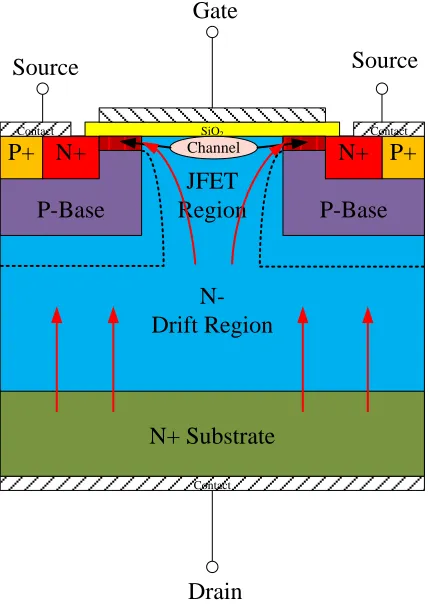
Figure 2.1 Power DMOSFET structure
From the structure shown in Figure 2.1, one can see that there is a parasitic NPN
off-14
state in all operating modes of the MOSFET otherwise this could lead to device latch-up
and loss of gate control. In order to satisfy this condition, the P-base region is shorted to
the source contact through the P+ region, as shown in Figure 2.1. Besides the parasitic
BJT in the structure, there is a P-N junction connecting the source region to the drain
region, which is called built-in body diode of the MOSFET. This body diode is usually
used as free-wheeling diode in some power electronic applications.
2.1.1
S
TATICI-V
C
HARACTERISTICSWhen a positive voltage is applied to the gate-to-source terminal, a conductive
electron channel is formed at the surface of the semiconductor under the gate and
connects the JFET region to N+ region at the source, as shown in Figure 2.1. This
channel provides an electron current flow path between drain and source. The
on-resistance during on-state is determined by the total on-resistance of the current path shown
in the figure, which is comprised of resistances of the N+ substrate, the N- drift region,
the JFET region, the channel resistance, and the N+ region connected to the source and.
Usually one can neglect the resistances in the N+ substrate and the N+ region that is
connected to the source because of the high doping concentrations in these regions. The
on-resistance is a very important parameter of the MOSFET because it determines the
current capability of the device [ 12 ]. It can be extracted from the slope of the I-V
15 Ron VBR In cr ea si n g V G S Saturation region Linear Region Drain-to-source Voltage D ra in -to -s o u rc e C u rr en t
Figure 2.2 I-V Characteristics of Power DMOSFET
When drain-to-source voltage VDS increases to a certain value, the device goes into the saturation region, where the drain-to-source current IDS saturates as shown in Figure 2.2. In this region device losses are high, since significant voltage and current are
both present at the same time. When the power MOSFET is working as a switch in
switching converter application, it is necessary to avoid the device operating in the
saturation region due to the limitation of high power dissipation of the device.
2.1.2
B
LOCKINGC
HARACTERISTICSPower MOSFET has positive blocking voltage capability. When the
gate-to-source voltage VGS is zero or negative, the device can support a large drain-to-source voltage VDS across the P-base/ N- drift region junction with a little leakage current going through the device (see the green line in Figure 2.2). Actually, during the off-state
operation, the depletion layer (see the black dashed line in Figure 2.1) extends out from
the P-base/ N-drift region junction to support the applied drain-to-source voltage. Figure
2.3 shows the depletion layer extension under off-state operation of power MOSFET for
16
MOSFET is not only limited by the thickness of the devices and the doping concentration
of N-drift region, but also by the structure inside the devices, such as the P-well spacing.
According to the discussion of advantages of material properties for SiC
compared with Si, SiC has almost 10 times larger critical breakdown electric field than
Si. From Equation 2-1 which is the expression of breakdown voltage of semiconductor
material, one can get almost 100 times higher breakdown voltage VBR for SiC-based device than for Si-based device for the same doping concentration.
D C SiC BR N q E V 2 2
Equation 2-1
JFET Region
N-Drift Region
P-Base P-Base
P+ N+ N+ P+
Contact SiO2 Contact
Contact N+ Substrate Gate Source Source Drain Channel
Low VDS
High VDS
Figure 2.3 Depletion layer extension of power MOSFET
2.1.3
D
YNAMICC
HARACTERISTICSThere are three major parasitic capacitances in power MOSFET, which are the
17
capacitance CDS, as shown in Figure 2.4. It is very important to accurately model the inner parasitic capacitances of power MOSFET in order to accurately capture its dynamic
characteristics, especially the modeling of the gate-to-drain capacitance (CGD), which affects the output switching waveforms due to the “Miller” effect. The dynamic behavior
of power MOSFET is usually dominated by the charging and discharging of the input
capacitance seen from the controlling gate terminal. Because of the Miller effect of
capacitance CGD, the equivalent input capacitance of the MOSFET will be the gate-to-source capacitance CGS in parallel with the amplified value of gate-to-drain capacitance
CGD during the switching transient.
CGS
CDS
CGD
Gate
Source Drain
Figure 2.4 Inner parasitic capacitances of power MOSFET
There are two methods to improve the switching speed of the power MOSFET.
One is reducing the gate resistance RG, the other one is minimizing the parasitic capacitances CGS and CGD. Reducing the gate-to-source capacitance shortens the charging and discharging time of the MOSFET and decreasing the gate-to-drain capacitance CGD reduces the Miller effect, so that the switching time can be faster.
Figure 2.5 shows the inner parasitic capacitances of a 1.2kV power MOSFET in
18
with increasing drain-to-source voltage. One can see that this Miller capacitance
decreases abruptly at low voltage, which affects the dynamic behavior of the MOSFET
severely during switching time. Therefore, in order to develop an accurate model for
power MOSFET, it is very important to take into account the non-linear gate-to-drain
capacitance CGD.
Figure 2.5 Inner capacitances of a 1.2kV power MOSFET in ATLAS simulation
2.2
P
OWERS
CHOTTKYD
IODEPower Schottky diode has a Metal-Semiconductor (MS) junction, as shown in
Figure 2.6. A metal–semiconductor junction is formed between a metal and a
semiconductor, creating a Schottky barrier. Unlike the power P-i-N junction, power
Schottky diode is majority carrier device which does not require a reverse recovery
current to discharge the minority carriers in the depletion region in the device. Therefore,
power Schottky diode is a very fast switching semiconductor device that can be used in
19
ND
Drift Region
n+ Substrate
Anode
Cathode
LD
Schottky Metal
Contact
Figure 2.6 Power Schottky diode structure
2.2.1
F
ORWARDC
HARACTERISTICSWhen a positive voltage is applied to the metal contact with respect to the N-type
semiconductor, the electrons in semiconductor side overcome the Schottky barrier to the
metal side creating the forward conduction current [ 12 ]. The forward current can be
calculated by using the thermionic emission theory.
Figure 2.7 Typical forward characteristics of power Schottky diode
⁄ ⁄
Equation 2-2
20
2.2.2
R
EVERSEC
HARACTERISTICSWhen a negative voltage VR is applied to the metal contact with respect to the N-type semiconductor, a depletion layer will be formed in the semiconductor side to support
the applied voltage. Since the N-type semiconductor holds all the blocking voltage, one
can also use Equation 2-1 to calculate the breakdown voltage of the power Schottky
diode at a certain doping concentration.
The leakage current of Schottky diode under reverse bias is also dominated by the
thermionic current across the Schottky barrier, which can be calculated by Equation 2-3.
From this equation, one can see that the leakage current of Schottky diode is dependent
on temperature. This limits power Schottky diode operation in high temperature
applications.
⁄ ⁄
Equation 2-3
2.2.3
P
OWERJ
UNCTIONB
ARRIERS
CHOTTKY(JBS)
D
IODEHigh performance switching converter applications require minimized conduction
loss and switching loss of power devices. Reducing the on-resistance of the device can
reduce the conduction loss of power Schottky diode, but this means the device has higher
doping concentration in drift region which corresponds to lower blocking voltage.
Therefore, there is a trade-off between on-resistance and blocking voltage in designing
the structure of power Schottky diode. Another way to reduce the conduction loss is to
decrease the Schottky barrier height. However, a lower barrier height will cause higher
leakage current during reverse bias and lower the maximum operating temperature of
21
The junction barrier Schottky diode (JBS) is a Schottky diode structure with a
P-N junction embedded into its P-N-drift region as shown in Figure 2.7. When a positive
voltage is applied to the metal contact with respect to the N-type semiconductor and this
voltage is not high enough to turn on the embedded P-i-N diode, the forward current just
goes through the Schottky part as seen in Figure 2.8.
ND
Drift Region
n+ Substrate
Anode
Cathode
LD
Schottky Metal
Contact
P+ P+
Figure 2.8 Power JBS diode structure
When a negative voltage is applied to the device, because of the existence of
P-well under the Schottky barrier, a depletion layer will be formed at the P-N junction that
will extend out to the current channel until the channel pinches off. After the channel
pinches off, the Schottky barrier is shielded by the potential formed by the depletion
layer. The further increase in the applied reverse bias is supported by the depletion layer
extending towards the N+ substrate. Once the Schottky barrier is shielded, the leakage
current stays almost constant, except for the little increasing current from the
space-charge generation of the P-N junction, which means that the leakage current is
independent of Schottky barrier height after pinch-off of the depletion layer. Therefore,
the JBS diode can have lower leakage current than conventional Schottky diode with the
22
JBS structure is not commonly used in Si-based Schottky diode because the
threshold voltage of the embedded P-i-N junction is just 0.7V which can make the diode
operate in minority carrier conductivity modulation (bipolar) mode when the P-N
junction turns on together with the Schottky barrier junction for a higher positive voltage
bias. For SiC Schottky diode with wider bandgap than Si, the threshold voltage of SiC
P-N junction is about 3V, which is higher than the Schottky barrier. Therefore, the Schottky
barrier junction inside the SiC JBS diode, which turns on during forwards conduction
mode, ensures that the P-N junction never turns on during this time.
2.3
S
UMMARYThis chapter briefly discusses the operation of power MOSFET and power
Schottky diode including the static characteristics and dynamic characteristics. Both of
these devices are majority carrier device with no minority carrier modulation during
conduction, which means fast switching speed during turn-off transient. Therefore, power
MOSFET and power Schottky diode can be used in high performance switching
23
CHAPTER 3
NEW PHYSICS- BASED SIC POWER DMOSFET MODEL
For switching converter applications at less than 200V, the silicon power
MOSFET has become the device of choice due to its low on-resistance and fast switching
speed. When designed for higher operating voltages, the use of silicon MOSFETs
becomes impractical due to the very high drift region resistance. Excellent electrical
properties of silicon carbide (SiC) material make it a very attractive semiconductor
material for power switching devices with capabilities that are superior to those of
devices based on silicon technology. In particular, 4H-SiC MOSFET is one of the most
promising candidates for high-speed and low-loss power switching applications.
Recently, SiC MOSFETs have become commercially available from Cree Inc.,
including single package and bridge module with voltage rating at 1.2kV. Therefore, it is
necessary to develop accurate models for SiC power devices so that electrical engineers
can evaluate the performance of SiC prototype devices in different applications and guide
the switching converter designs.
In this chapter, a new circuit-based SiC DMOSFET model that physically
captures the mechanism of current saturation in power SiC DMOSFET is developed in
PSpice software based on finite element simulation results. A significant advantage of the
model is that a single set of equations describes operation in both the linear and saturation
non-24
uniform current distribution in the JFET region that causes current saturation, as shown
by the finite element simulations. Finally, the model is validated by comparing simulated
results with experimental results both under static and dynamic conditions.
3.1
L
ITERATURER
EVIEW OFS
IC
MOSFET
M
ODELINGAs mentioned above, device models can be divided in two major groups: 1)
analytical models based on the finite element solution of drift-diffusion carrier transport
in two or three dimensions [ 14 ]- [ 16 ]; and 2) circuit-oriented models which employ
equation-based description of device behavior. While extensive research has been done to
develop analytical models for SiC MOSFET [ 24 ]- [ 26 ], there are very few publications
addressing the implementation of circuit-oriented models in simulators such as PSpice
[ 27 ]- [ 28 ].
The physics- based numerical model in [ 24 ], which accounts for incomplete
ionization and the charging and discharging of interface states, is based on the drift-
diffusion equations. This model could reveal the effects of surface phenomena, but it is
quite complex and would require long simulation times. Moreover, the model is not
suitable for implementation in a circuit simulator due to its complexity. The model
presented in [ 28 ] is a simple SPICE behavioral model for SiC power DMOSFETs. The
model is obtained by introducing specific modifications to the conventional level-1 Si
power MOSFET model available in commercial SPICE simulators. The model in [ 27 ] is
based on the latest version of the power MOSFET model utilized in the Hefner IGBT
model [ 29 ], where the parameters of both the Si and SiC MOSFETs can be extracted
25
models need to extract several fitting factors from device experimental output
characteristics to obtain good matching.
3.2
F
INITEE
LEMENTS
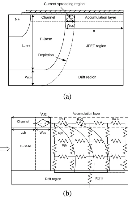
IMULATIONTypical structure of a power SiC DMOSFET is shown in Figure 3.1. The physical
dimensions and doping concentrations are for a 1.2kV device. It is a vertical device with
a planar gate, the channel has a 1µm length and the drift region has a 10µm thickness.
Applying a positive voltage to the gate larger than the threshold voltage, an inversion
layer is created on top of the p-base region, forming an n-type conducting channel
connecting the source to the JFET region. At the same time, an accumulation layer is
formed under the gate oxide at the top of the JFET region, providing current spreading
for the electron current flowing from the channel into the JFET region. For small values
of drain-source voltage (linear or triode region), the device exhibits an approximately
constant on-state resistance, which is determined by channel and drift region resistances.
Ultimately, at a higher drain-source bias, the current saturates (saturation region). From
standard analysis of power MOSFETs, it is known that there are at least three
mechanisms that can contribute to current saturation in power MOSFET: channel
pinch-off, carrier velocity saturation in high-electric-field regions, and the so-called parasitic
JFET effect, i.e., the fact that the current does not flow uniformly in the JFET region but
is constrained to flow in a narrow JFET channel. According to performed finite element
simulations, carrier velocity saturation at the interface between the channel and the JFET
region is the main reason for current saturation for the SiC DMOSFET structure of Figure
3.1. The JFET effect is also a significant contributing factor. The proposed physics-based
26
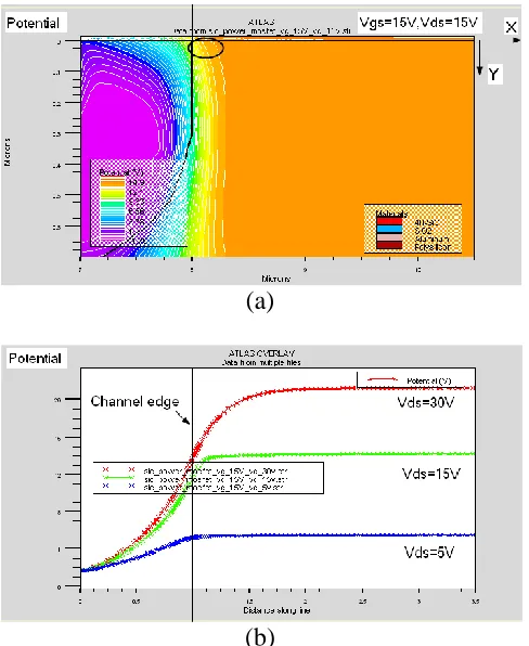
Figure 3.1 Structure of power SiC DMOSFET
Figure 3.2 shows the forward I-V characteristic obtained from finite element
simulation of the device structure of Figure 3.1 using Silvaco ATLAS [ 31 ]. Gate-source
voltage is constant (15V) for all drain-source voltages, ensuring that the device is fully
on. Three values of drain-source voltage are considered: VDS=5V, 15V and 30V. For
VDS=5V the device operates in the linear region, and for VDS=15V, 30V it operates in the saturation region.
Figure 3.2 I-V characteristic of DMOSFET for VGS=15V obtained from finite element simulation.
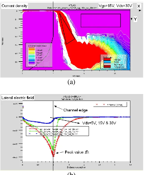
Figure 3.3 (a-b) shows the current density distribution in a rectangular region
27
VDS=30V. This region extends for 2µm in the x-direction and for 0.035µm in the y-direction and is identified by the small hatched rectangular region in Figure 3.1. Notice
that the thickness and the shape of the channel are very similar for the two drain-source
voltages and no significant pinch-off is observed even when the device is in deep
saturation (VDS=30V). This shows that channel pinch-off is not a significant contributor to current saturation. The biggest difference between Figure 3.3 (a) and Figure 3.3 (b) is
that for operation in the saturation region a depletion region forms in the JFET region and
the current flows along a narrow vertical path adjacent to the p-base.
(a)
(b)
Figure 3.3 Finite element simulation results. Current density two-dimensional distribution along the channel for operation in the linear region, VDS=5V (a) and in the
28
Figure 3.4 (a) shows two-dimensional finite element simulation results for the
electric potential in the upper part of the SiC DMOSFET (rectangular dashed region in
Figure 3.1). Figure 3.4 (b) shows the electric potential curve on a cutline along the
channel (cutline: X=7µm-10.5µm, Y=1nm) for the three values of drain-source voltage of
Figure 3.2. Figure 3.5 (a) shows the two-dimensional current transport and Figure 3.5 (b)
shows the lateral (x-axis) electric field component along the same cutline.
From these simulation results one can draw some conclusions on saturation
mechanism in a typical power SiC DMOSFET. Pinch-off of the channel was not
observed under any drain-source bias: even at VDS=30V the channel retains its approximately rectangular shape and does not display channel pinch-off condition.
Additional confirmation of this can be obtained by looking at Figure 3.4 (b), which shows
that the potential drop in the channel does not change much (from 12V to 14V
approximately) as VDS increases from 15V to 30V. This shows that most of the voltage drop across the device in saturation does not occur in the channel, but somewhere else (in
the JFET region). As the drain-source voltage increases, the lateral electric field shown in
Figure 3.5 (b) becomes quite large at the end of the channel, where it reaches its peak
value Ek when current goes to saturation regime. Detailed investigation of carrier transport in the channel region as predicted by the finite element simulations reveals that
29 (a)
(b)
Figure 3.4 Finite element simulation results. (a) Electric potential two-dimensional distribution for VGS=15V, VDS=15V and (b) electric potential along cutline for three
drain-source voltages.
Traditionally, it is assumed that an accumulation layer is always formed under the
gate oxide in the JFET region and further analysis of current transport in power MOSFET
is based on this assumption. This accumulation layer helps spreading the electron current
coming from the channel uniformly across the undepleted portion of the JFET region. As
a result, the JFET region can be represented as a rectangular piece of semiconductor
material whose width is modulated by change of depletion region width of p-base/n-JFET
junction, with electron current flowing vertically from the JFET accumulation layer under
the gate to the drift region. However, the finite element simulation of Figure 3.5 (a) tells a
different story: the current distribution in the JFET region is highly non-uniform and
30
layer (see triangular region in Figure 3.5 (a) for VDS = 30V). Notice that the accumulation layer disappears in the JFET region and is replaced by a depletion region (rectangular
region in Figure 3.5 (a)). Notice also that the electric potential increases sharply at the
end of the channel with drain voltage increasing. A significant portion of the voltage drop
is localized in the current spreading region across the depleted portion of the JFET region
(see circled region in Figure 3.4 (a)). So one can divide the JFET region into two parts:
one is the current spreading region across the depleted portion, with electron current
spreading out laterally; the other is the triangular region mentioned before, with electron
current flowing vertically and non-uniformly. Based on this idea, a new circuit-based
model is developed, which physically represents the mechanism of current saturation in
power SiC DMOSFET.
(a)
(b)
31
The physical treatment of current spreading in DMOSFET proposed by Baliga
considers accumulation and JFET region as two individual regions [ 12 ]. Resistance of
accumulation region is determined by gate voltage only, while resistance of JFET region
is a function of drain-source voltage only. However, based on the performed
finite-element investigation, the resistance of the accumulation region is a strong function of
both VGS and VDS, which is not considered in classical solutions for current transport of power DMOSFET. Moreover, the resistance of JFET region is not only determined by
depletion width of p-base/JFET junction, but also and more predominantly by reduction
of current conduction in the central part of JFET region caused by formation of a
depletion region between adjacent p-base regions (rectangular region in Figure 3.5 (a)).
For large values of gate-source voltage, such as the VGS=15V case, the JFET current channeling effect is significant only for large values of drain-source voltage, such as the
VDS=30V case of Figure 3.5 (a), which are not of great practical interest, since power dissipation is exceedingly large. However, for smaller values of gate-source voltage, this
effect becomes significant at correspondingly lower values of drain-source voltage. For
this reason it is important to capture this effect in order to have an accurate device model.
3.3
N
OVELM
ODEL WITHN
ON-
UNIFORMC
URRENTD
ISTRIBUTION IN THEJFET
R
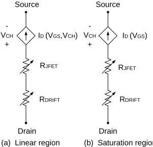
EGIONThe simple standard model of a power MOSFET is a piecewise model using
different equations to describe operation in the linear region and saturation region. The
two equivalent circuits are shown in Figure 3.6. For simplicity device capacitances and
32
dependent on both gate- source voltage VGS and channel voltage VCH. When VCH ≥
VCH,SAT, the MOSFET operates in the saturation region and ID is a function of VGS only and does not depend on VCH. So there are two different equations for current ID in the standard model, one for the linear region and another one for the saturation region.
Source
-VCH
+
ID (VGS,VCH)
RJFET
RDRIFT
Drain
(a) Linear region
Drain RDRIFT
RJFET
ID (VGS)
-VCH
+ Source
(b) Saturation region
Figure 3.6 Standard power MOSFET static model structure.
For linear region, the drain current ID is given by
2
0 2
2 CH GS T CH CH
OX CH
D V V V V
L Z C
I Equation 3-1
For saturation region, the drain current ID is
2 , 0
2 CH CHSAT OX CH DSAT V L Z C
I Equation 3-2
The nonlinear resistors RJFET and RDRIFTare given by
) (
2 JFET JFET JFET
JFET JFET W a Z N q L R
Equation 3-3
DRIFT DRIFT drift n DS DRIFT DRIFT W Z N q W L R
2 Equation 3-4
The structure of the new proposed model is shown in Figure 3.7. It consists of
33
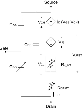
drift resistance RDRIFT, and capacitances CGS, CDS and nonlinear capacitance CGD. The novelty of this model is in how the JFET region is modeled by VJ2 and RJ_net.
+ -Source Drain Gate CGS CGD CDS -VCH +
ID (VGS,VCH)
-VJ2 + -VJ1 + RJ_net RDRIFT -VJFET + ID
Figure 3.7 Proposed SiC DMOSFET model structure.
Taking into account that SiC MOSFET current saturation is due to a large voltage
drop in JFET region and not to channel pinch- off, it is possible to use only one equation
to describe the channel region forward I-V characteristic. This is the equation
corresponding to linear region of operation in the standard model of Figure 3.6:
2
2
2 CH GS T CH CH
OX CH
D V V V V
L Z C
I Equation 3-5
Thus, channel region is represented by a voltage-controlled current source and
channel voltage VCH can be determined by subtracting voltage drop in JFET and drift region from total voltage applied to the device:
DRIFT D JFET DS
CH V V I R
V Equation 3-6
34 DRIFT DRIFT drift n DS DRIFT DRIFT W Z N q W L R
2 Equation 3-7
) ( 2 JFET CH bi DRIFT sic
DS V V V
N q
W
Equation 3-8
where VJFET is the voltage drop in JFET region.
3.3.1
JFET
R
EGIONM
ODELINGThe proposed method to capture the current saturation in the discussed
DMOSFET is to represent JFET region as two parts: a voltage source and a matrix of
resistors as in Figure 3.7. The specific structure is shown in Figure 3.8. Voltage source
VJ2 represents the voltage drop in the current spreading region and the resistor network allows for a non-uniform current distribution in the JFET region. This approach takes into
account JFET region voltage drop in both lateral and vertical directions, therefore
capturing the two-dimensional nature of current spreading in this region. The top row of
resistors represents the accumulation layer while the remaining matrix resistors represent
the main body of JFET region. The main feature of this approach is that values of the
resistors in the accumulation layer are function of both VGS and VDS. Let us consider a resistor Rai in the top row. Due to the voltage drop on the resistors to its left, the voltage