Available online: https://edupediapublications.org/journals/index.php/IJR/ P a g e | 29
Proposal of a Novel Test Application Strategy for Optimum
Power Utilization and Achieving Minimum Number of
Transitions
Prof.Dr.G.Manoj Someswar
1, Babu Rajesh
21. Research Supervisor, Dr.APJ Abdul Kalam Technical University, Lucknow, U.P.,
India
2. Research Scholar, Dr.APJ Abdul Kalam Technical University, Lucknow, U.P., India
Abstract
Testing low power very large scale integrated (VLSI) circuits in the recent times has become a critical
problem area due to yield and reliability problems. This research work lays emphasis on reducing power
dissipation during test application at logic level and register-transfer level (RTL) of abstraction of the
VLSI design flow. In the initial stage, this research work addresses power reduction techniques in scan
sequential circuits at the logic level of abstraction.
Implementation of a new best primary input
change (BPIC) technique based on a novel test
application strategy has been proposed. The
technique increases the correlation between
successive states during shifting in test vectors
and shifting out test responses by changing the
primary inputs such that the smallest number of
transitions is achieved. The new technique is test
set dependent and it is applicable to small to
medium sized full and partial scan sequential
circuits. Since the proposed test application
strategy depends only on controlling primary
input change time, power is reduced with no
penalty in test area, performance, test efficiency,
test application time or volume of test data.
Furthermore, it is indicated that partial scan
does not provide only the commonly known
benefits such as less test area overhead and test
application time, but also less power dissipation
during test application when compared to full
scan. With a view to promote for power savings
in large scan sequential circuits, a new test set
independent multiple scan chain-based technique
which employs a new design for test (DFT)
architecture and a novel test application strategy
has been indicated in this research work. The
technique has been validated using benchmark
examples and it has been shown that power is
reduced with low computational time, low
overhead in test area and volume of test data and
with no penalty in test application time, test
efficiency, or performance. The second part of
this dissertation addresses power reduction
techniques for testing low power VLSI circuits
using built-in self-test (BIST) at RTL. First, it is
Available online: https://edupediapublications.org/journals/index.php/IJR/ P a g e | 30 associated with traditional BIST methodologies.
It is shown how a new BIST methodology for
RTL data paths using a novel concept called test
compatibility classes (TCC) overcomes high test
application time, BIST area overhead,
performance degradation, volume of test data,
fault-escape probability, and complexity of the
testable design space exploration. Secondly,
power reduction in BIST RTL data paths is
achieved by analyzing the effect of test synthesis
and test scheduling on power dissipation during
test application and by employing new power
conscious test synthesis and test scheduling
algorithms. Thirdly, the innovative BIST
methodology has been validated using
benchmark examples. Also, the research work
states that when the power conscious test
synthesis along with the test scheduling is
combined with novel test compatibility classes
and in this proposed research work,
simultaneous reduction in test application time
and power dissipation is achieved with low
overhead in computational time.
Keywords
: Testing low power very large scaleintegrated (VLSI), Register-transfer level (RTL),
Test compatibility classes (TCC), Built-in self-test
(BIST), Best primary input change (BPIC) Linear
feedback shift register (LFSR)
cuits with no penalty in area overhead, test application time, test efficiency, performance, or volume of test data. However, the computation of the best primary input change (BPIC) time introduced research paper is dependent on the size and the value of the test vectors in the test set. Therefore, integrating the proposed best
primary input change time with scan cell and test vector ordering leads to discrete, degenerate and highly irregular design space, and hence high computational time, which limits the applicability of the new BPIC test application strategy only to small to medium sized scan sequential circuits?[1] This chapter introduces a new test set independent technique based on multiple scan chains and shows how with low overhead in test area and volume of test data, and with no penalty in test application time, test efficiency, or performance, considerable savings in power dissipation during test application in large scan sequential circuits can be achieved in low computational time. Further, the extra test hardware required by the proposed technique employing multiple scan chains can be specified at the logic level and synthesised with the rest of the circuit. This makes the proposed multiple scan chains-based power minimisation technique easily embeddable in the existing VLSI design flow as described previously in Figure 1.
Available online: https://edupediapublications.org/journals/index.php/IJR/ P a g e | 31 cells in multiple scan chains based on their
classification, and a new test application strategy based on the DFT architecture described in the previous section are introduced in research paper. Experimental results and a comparative study of the proposed BPIC and the multiple scan chain-based technique are presented.
Motivation and Objectives
The aim of this chapter is to reduce power dissipation in large scan sequential circuits. Despite their benefits in lowering power dissipation during test application, the previously described techniques, and the new BPIC test application strategy, also described in, are inefficient for large scan sequential circuits due to one or more of the following problems:
a. test area overhead associated with detection logic required to find non-essential vectors (i.e. vectors which do not contribute to an increase in fault cover-age).
b. performance degradation associated with modified scan cell design.
c. large test application time required to achieve significant power savings.
d. clock tree power dissipation is tackled by clock gating only for nonessential test vectors.
e. high number of extra test vectors emerges as a problem to testers which need to change to support the large volume of test data.
f. computational time may be prohibitively large hindering the exploration for large sequential circuits.
The aim of this chapter is to introduce a new technique for power minimisation during test application in large scan sequential circuits based on a novel DFT architecture which eliminates all the above mentioned problems (a) - (f). The proposed DFT architecture is based on partitioning scan cells into multiple scan chains which reduces the clock tree power dissipation and does not have performance penalty. A new test application strategy for the proposed DFT architecture which applies a single extra test vector while shifting out test responses for each scan chain is presented. The multiple scan chain-based approach for power minimisation which is test set independent, is applicable to both non-compact and compact test sets leading to low test application time. It is shown that with low overhead in test area and volume of test data, and with no penalty in test application time, test efficiency, or performance, high savings in power dissipation during test application in large scan sequential circuits are achieved in low computational time.
Background and Definitions
Available online: https://edupediapublications.org/journals/index.php/IJR/ P a g e | 32 set of connected gates and wires. A path is
defined by a single input wire and a single output wire per gate. A signal is an on-input
if it is on the target path. A signal is an off-input (side input) if it is an input to a gate which is on a target path but is not an on-input. If two faults can be detected by a single test vector,
they are compatible faults. Consequently, two faults are incompatible, if they cannot be detected by a single test vector. A test vector from a given test set is an essential test vector, if it detects at least one fault that is not detected by any other test vector in this test set. A test vector is non-essential with respect to a given test set if all the faults detected by it are also detected by other test vectors in the given test set. A test set independent approach for power minimisation depends only on circuit structure and savings are guaranteed regardless of the size and the value of the test vectors in the test set. This is unlike the test set dependent approaches, where power minimisation depends on the size and the value of the test vectors in the test set, as introduced.[3]
Power
Minimisation
in
Scan
Sequential Circuits Based on Multiple
Scan Chains
In this section a new technique for power minimisation in large scan sequential circuits based on multiple scan chains is introduced. Overviews the proposed DFT architecture for power minimisation. It defines compatible, incompatible, and independent scan cells and their importance for partitioning scan cells
into multiple scan chains. It gives an important theoretical result showing the advantage of the proposed DFT architecture from the clock tree power dissipation standpoint, and describes how the proposed multiple scan chains can be extended to scan BISTmethodology.[4]
Proposed
Design
for
Testability
Architecture Using Multiple Scan
Chains
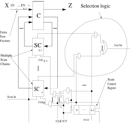
The proposed DFT architecture using multiple scan chains SC0: : :SCk 1is illustrated in Figure 4.1. The scan input Scan In is routed to all scan chains while the scan output Scan Out is selected from the output of each scan chain. Scan chains SC0: : :SCk
1are operated using non-overlapping enable signals for clocks CLK0: : :CLKk 1. Non-overlapping enable signals gate the system clock CLK using a scan control register where the number of cells equals the number of scan chains. This implies that scan chains
SC0: : :SCk 1are enabled one by one during each scan cycle. While shifting out test responses through scan chain SCi, only the
Available online: https://edupediapublications.org/journals/index.php/IJR/ P a g e | 33 extra logic are observable through Scan Out
line using the test data which is shifted through the k scan chains and control data shifted through the scan control register. Therefore, the extra test hardware, including the selection logic shown in Figure 1, has no penalty on test efficiency. During the normal operation of the circuit CLK0: : :CLKk 1are active at the same time, since when normal/test signal N=T is 1 the outputs of the extra OR gates are 1 and CLK is not gated by the scan control register.
To provide a brief overview of the test application strategy for the proposed DFT architecture, while shifting out test responses present in scan cells within scan chain SCi,
primary inputs are set to extra test vector EVi
which eliminates the spurious transitions that originate from scan cells within scan chain
SCi. The number of clock cycles required to
shift in the present state (pseudo input) part of each test vector equals the number of scan cells and the test response is loaded in a single clock cycle. This implies that there are no extra clock cycles for each test vector applied to the circuit under test and hence no penalty on test application time. Note that the proposed DFT architecture has no penalty on performance, since extra test hardware is not inserted on critical paths. Further, the extra test hardware required by the scan control
register and selection logic can be specified at the logic level and synthesised with the rest of the circuit which makes the proposed DFT architecture easily embeddable in the existing VLSI design flow. It should be noted that the proposed DFT[5] architecture introduced for full scan sequential circuits is equally applicable to partial scan sequential circuits. Since the number of scan cells in a partial scan sequential circuit is approximately 10% of the total number of state elements it is more appropriate to illustrate the applicability of the proposed architecture on large full scan sequential circuits. However, as the complexity of state of the art digital circuits increases it is expected that in the foreseeable future partial scan sequential circuits with very high number of scan cells will appear. In such cases, the technique proposed in this chapter
is applicable with no modifications to partial
scan sequential circuits. What makes the proposed multiple scan chain-based DFT architecture particularly suitable for large scan sequential circuits is that partitioning scan cells into multiple scan chains is test set independent, and it depends only on the circuit size and structure unlike the solutions described in the previous Chapter 3 which strongly rely on the size of the test set and hence are applicable only to small to medium sized scan sequential circuits.
Available online: https://edupediapublications.org/journals/index.php/IJR/ P a g e | 34
X
<EV
... EV >
Z
Selection logic
0 k-1
C
Extra
Test
Vectors
SC
Scan Outk-1
Multiple
Scan
CLK k-1Chains
Scan
SC
Control
Register
0
Scan In
CLK0
0 k-1
CLK N/T SCLK
Figure 1: Proposed DFT architecture based on multiple scan chains.
Compatible, Incompatible, and Independent Scan Cells
In order to partition scan cells into multiple scan chains, they need first to be classified into three broad classes: compatible, incompatible, and independent scan cells. It should be noted that scan cell classification is not done explicitly by enumeration or exhaustive search, but it is done implicitly by the multiple scan chains partitioning algorithm as explained later in
Available online: https://edupediapublications.org/journals/index.php/IJR/ P a g e | 35 Definition 1 A spurious transition during test
application in scan sequential circuits is a transition which occurs in the combinational part of the circuit under test while shifting out the test response and shifting in the present state part of the next test vector.[6] These transitions do not have any influence on test efficiency since the values at the input and output of the combinational part are not useful test data. Now the compatible and incompatible scan cells are introduced.
Definition 2 Two scan cells Si and S j are compatibleif all primary inputsxk are as-signed
values ck that eliminate the spurious transitions
which originate from both Si and Sj . The values ck of primary inputs xk constitute the extra test vector which eliminates spurious transitions originating from both Si and Sj.[7]
Note that the sole purpose of extra test vectors is to reduce the spurious transitions during test application and has no effect on fault coverage which is determined by the original test set. The application of extra test vectors defines a novel test application strategy for power minimisation which is detailed. Further, since a single extra test vector is used for each scan chain regardless of values loaded in scan cells then the volume of extra test data is dependent only on the number of scan chains and not on the number of scan cells and/or the size of the original test set.
Definition 3 Two scan cells Si and S j are incompatibleif at least one primary inputxkthat
is assigned value ik to eliminate the spurious
transitions which originate from Si will propagate
the transitions which originate from S j . Two
incompatible scan cells cannot be assigned to the same scan chain since there is no extra test vector that can eliminate spurious transitions which originate from both of them.
The following example illustrates compatible and incompatible scan cells.
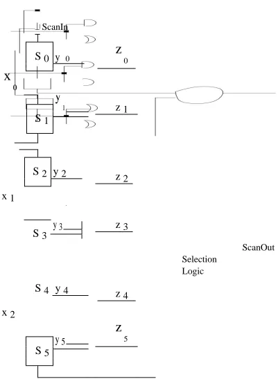
Example 1 Consider the circuit shown in Figure 2. The fx0;x1;x2g are primary in-puts,
fS0;S1;S2;S3;S4;S5g are scan cells,
fy0;y1;y2;y3;y4;y5g are present state lines, and
fz0;z1;z2;z3;z4;z5g are circuit outputs. To eliminate
spurious transitions at gate z0 while shifting out
test responses through scan cell S0, primary input x0 must be assigned the con-trolling value 0 of
gate z0. Similarly, to eliminate spurious
transitions that originate from scan cell S1,
primary input x0 must be assigned the controlling
value 1 of gate z1. Different values must be
assigned to x0 to eliminate spurious transitions
which originate from scan cells S0 and S1.
Therefore scan cells S0 and S1 are incompatible
and are assigned to different scan chains SC0=
fS0g and SC1 = fS1g. On the other hand, by
assigning x1 to the controlling value 0 of gates z2
and z3 the spurious transitions which originate
from both scan cells S2 and S3 are eliminated.
Thus, by introducing S2 and S3 into SC0 and
applying for example extra test vector x0x1x2 =
f000g while shifting out test responses from SC0
=fS0;S2;S3g no spurious transitions will occur at
gates z0, z2 and z3. Similarly, scan cells S4 and S5
are compatible since assigning 1 to the primary input x2 eliminates spurious transitions at gates z4
and z5. By introducing S4 and S5 into SC1 and
applying extra test vector x0x1x2 = f111g while
shifting out test responses from SC1=fS1;S4;S5g
Available online: https://edupediapublications.org/journals/index.php/IJR/ P a g e | 36 and z5. It should be noted that there is a strict
interrelation between extra test vector value
x0x1x2 =f000g and scan chain SC0 =fS0;S2;S3g,
and x0x1x2 = f111g and scan chain SC1 =
fS1;S4;S5g. While for thesake of simplicity, the
extra test vectors x0x1x2 = f000g and x0x1x2 =
f111g were de-scribed explicitly in this particular example, the extra test vectors and hence the multiple scan chains, are derived implicitly by the partitioning algorithm as explained later in Figure 9. Finally, note that output signals z3 of
scan chain SC0 and z5 of SC1 are fed into the
selection logic of the proposed DFT architecture from Figure.1. The previous example has assumed a simple circuit where all the spurious transitions are eliminated by partitioning scan cells in two scan chains SC0 and SC1. However,
some of the spurious transitions cannot be eliminated as described in the following example.[7]
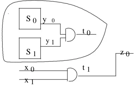
Example 2 Consider the circuit shown in Figure 3. The spurious transitions which originate in scan cells S0 and S1 cannot be eliminated at gate t0 since both inputs are present state lines.
However, by assigning x0 and/or x1 to the
controlling value 0 of gate t1 the spurious
transitions will be eliminated at gate t1. Scan
cells S0 and S1 are compatible since same
primary input values eliminate the spurious transitions of gate t1.
Example 3 has illustrated that some of the spurious transitions cannot be eliminated since all the gate inputs depend on present state lines. Computing primary input values that eliminate spurious transitions (extra test vectors introduced in Definition 2) can be viewed as an ATPG
problem to a reduced circuit with a specified fault list which are detailed in the algorithms presented. The following Example 3 briefly illustrates the generation of the reduced circuit
Available online: https://edupediapublications.org/journals/index.php/IJR/ P a g e | 37
ScanIn
y
S
0
0
z
0
x
0
y
1
z
1
S
1
y
2
S
2
z
2
x
1
y
3
z
3
S
3
ScanOut
Selection
Logic
S
4
y
4
z
4
x
2
y
5
z
5
S
5
Figure 2: Example 1 circuit illustrating compatible and incompatible scan cells
S
0
y
0
y
1
t
0
z
0
S
1
Available online: https://edupediapublications.org/journals/index.php/IJR/ P a g e | 38
x
0
t
1
x
1
Figure 3: Example 2 circuit illustrating spurious transitions which cannot be eliminated on
t
0.
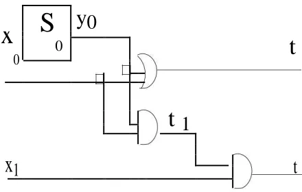
S
0
y
0t
0
S
1
y
1
z
0
x
0
t
1
x
1
Figure 4: Reduced circuit of the example circuit from Figure 3 illustrating the steps required to
compute extra test vectors
Example 4 For the circuit shown in Figure3the reduced circuit is generated as follows using the part (a) of the algorithm shown in Figure 9. Initially the signal t1 at the input of gate z0 is
identified to eliminate spurious transitions that originate from scan cells S0 and S1. Then scan
cells S0 and S1, and the AND gate t0 are excluded
from the reduced circuit as shown in Figure 4. Furthermore, gate z0 is modified to a buffer
(signals t1 and z0 are identical). The targeted fault
in the reduced circuit is t1stuck-at 1 (sa 1) which
eliminates the spurious transitions at gate z0 in
the original circuit. Finally, the extra test vectors (Definition 2) that eliminate the spurious transitions during test application are computed
x0x1=f0X;X 0g.
A particular case of scan cells are self-incompatible scan cells which are defined as follows.
Definition 4 A scan cellSiisself-incompatibleif
at least one primary input xk that is assigned
value ik to eliminate the spurious transitions
which originate from Si on one fan out path will
propagate the transitions which originate from Sj
on a different fan out path. Now a new question which arises is whether the spurious transitions
which originate from self-incompatible scan cells can be eliminated? In order to provide an answer consider the following example.
Example 5 Consider the circuit of Figure 5 wherefx0;x1gare primary inputs,S0isscan cell, y0 is present state line, and ft0;t1;t2g are circuit
Available online: https://edupediapublications.org/journals/index.php/IJR/ P a g e | 39 while shifting out test responses through scan
cell S0, primary input x0 must be assigned the
controlling value 1 of gate t0. However, to
eliminate spurious at gate t1, primary input x0
must be assigned the controlling value 0 of gate
t1. Different values must be assigned to x0 to
eliminate spurious transitions which originate from the same scan cell S0 and hence scan cell S0
is self-incompatible. However if primary input x1
is assigned the controlling value 0 of gate t2the
spurious transitions which originate in S0 and
propagate on path fS0;t1;t2g will be eliminated.[9]
Therefore by assigning extra test vector x0x1 =
f10g, the spurious transitions propagating on both paths fS0;t0g and fS0;t1;t2g will be
eliminated. This leads to the conclusion that most of the spurious transitions originating in self-incompatible scan cells can be eliminated by examining the fan out paths of self-incompatible scan cells and assigning a single extra test vector while shifting out the test responses. However, the single extra test vector is at the expense of a small number of spurious transitions that cannot be eliminated as in the case of transitions on line
t1 in the simple circuit of Figure5.
The previous example has shown that following a careful examination of fan out branches of self-incompatible scan cells, most of the spurious transitions originating in self- self-incompatible scan cells can be eliminated using a single value for the extra test vector. Finally, independent scan cells are introduced.[8]
Definition 5 A scan cellsSiisindependentif all the gates on all the paths which originate from Si do not
have at least one side input which can be justified by primary inputs.
y
0
S
0
x
0
t
1
t
t
x
1
Figure 5: Example 4 circuit illustrating self-incompatible scan cells
The independent scan cells are grouped in the extra scan chain (ESC) for which no extra test vector can be computed and hence the spurious transitions cannot eliminated. The following example illustrates independent scan cells.
Example 5 Consider the circuit shown in Figure6. Outputz0depends only on scancells S0 and S1, and
Available online: https://edupediapublications.org/journals/index.php/IJR/ P a g e | 40 gates t0 and t1 that can be justified by primary inputs such that spurious transitions originated from S0, S1, S2 and S3 are eliminated. Therefore scan cells S0, S1, S2 and S3 are independent.
S
0
y
0t
0
z
0
y
1
S
1
y’
4
S 4 y 4
S
2
y
2
t
1
y
3
S
3
Figure 6: Example 5 circuit illustrating independent scan cells.
Power Dissipated by the Buffered Clock Tree
Previous research has established that power dissipated in the clock tree is typically one third of the total power dissipation and hence it is necessary to minimise power dissipated in the clock tree not only during functional operation but also during test application. Unlike previous approaches which do not consider power dissipated by the buffered clock tree or gate the clock tree only for non-essential test vectors from a large test set, the proposed DFT architecture using multiple scan chains (Figure 1 ) reduces clock tree power for all the test vectors of a very small test set where each test vector is essential (i.e. detects at least one fault). This is explained by the following theorem which gives an upper bound on power reduction.[10]
Theorem 1 Considerkscan chains in the DFT architecture of Figure1 thenthe power reduction of the buffered clock tree over the standard full scan architecture is upper bounded by (k 1)=k.
k 1
Proof
: Let f
m
0
; : : : ;
m
k
1
g
be the size of each scan chain and
å
m
i
=
m
, where
m
is the
i=0
total number of scan cells. Since for large dies the clock power dissipation changes from square-root dependence on the number of scan cells to a linear dependence power dissipated by each scan chain SCi can be approximated
to mi where is dependent on clock frequency, supply voltage and wire lengths. The power dissipated while
shifting test responses over an entire scan cycle (m clock cycles) for the proposed architecture
1
is
P
MSC
=
å m
2
i
since over
m
i
clock cycles only the buffered clock tree feeding
SC
i
i=0is active. On the other hand power dissipated in the traditional full scan architecture is
k 1 k 1
Available online: https://edupediapublications.org/journals/index.php/IJR/ P a g e | 41
i=0 i=0
1 k 1 k 1
Red
= (
P
FU LL
P
MSC
)=
P
FU LL
=
1
(
å
m
i
2
)=(
(
å
m
i
) (
å
m
i
))
.
i=0 i=0 i=0
Following Cauchy-Schwarz inequality where
k 1 k 1 k 1
(
å
m
i
) (
å
m
i
)
kfi
(
å
m
2
i
)
i=0 i=0 i=0
the power reduction is upper bounded by
Red
ffi
1
1
=
k
= (
k
Available online: https://edupediapublications.org/journals/index.php/IJR/ P a g e | 42 The previous theorem shows that power reduction of up to (k 1)=k can be achieved in the buffered clock tree,
with maximum reduction achieved when scan chains have an equal number of scan cells. It should be noted that
by gating the clock of each scan chain not only average power reduction is achieved but also savings in peak
power are guaranteed since while shifting out test responses only a single buffered clock tree is active.
Extension of the Proposed DFT Architecture Based on Multiple Scan Chains to Scan BIST
Methodology
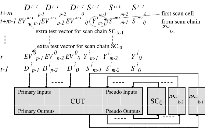
So far the proposed DFT architecture based on multiple scan chains introduced. It was applied to full scan sequential circuits using external automatic test equipment ATE (Figure1). This can be summarised in Figure 7 where the extra test vectors for scan chains SC0 and SCk 1are highlighted. Further, it is shown that the test response Ymi 1, which is the test response in the first scan cell from scan chain SCk 1, has yet to be shifted after the test responses from scan chains SC0; : : : ;SCk 2 were already shifted out.
Time
t+m
D
i+1
D
i+1D
i+1S
i+1S
i+1S
i+1first scan cell
p-1 p-2 0 m-1 m-2 0
t+m-1 EV
k-1p-1EV
k-1p-2EV
k-1 0Y
im-1S
i+1 m-1S
i+10 from scan chainextra test vector for scan chain SC k-1
SC
k-1extra test vector for scan chain SC 0
t
EV
0p-1EV
0p-2EV
00Y
im-1Y
im-2Y
i0t-1
D
ip-1D
ip-2
D
i 0
S
i m-1
S
i
m-2
S
i
0
Primary Inputs Pseudo Inputs
CUT
SC0
SC
k-2SC
k-1
Primary Outputs
Pseudo Outputs
Figure 7: Summary of the proposed DFT architecture based on multiple scan chains when
Available online: https://edupediapublications.org/journals/index.php/IJR/ P a g e | 43 However, the proposed DFT architecture based on multiple scan chains is not applicable only to standard scan sequential circuits using external ATE [11]. In the following the minor modifications which need to be considered when using scan BIST methodology (Figure 1 is given. Figure 8 shows that the serial output of the linear feedback shift register (LFSR) is fed directly into the scan chain which makes the primary inputs directly controllable while shifting out test responses from each scan chain. Therefore, extra test vectors associated with each scan chain can be applied to primary inputs while shifting in the present state part of the next test vector associated with each scan chain. Scan cells are partitioned into multiple scan chains and extra test vectors are calculated in the same way as for scan sequential circuits as described in the following. This will lead to a lower area overhead associated with scan BIST methodology (Figure 5) at the expense of higher interference from ATE which needs to store the primary input part of each test vector and the extra test vector associated with each scan chain.
counter
LFSR
extra
test vector
for each
p
N/T
scan chain
Primary Inputs
Pseudo Inputs
Multiple
CUT
scan chains
Primary Outputs Pseudo Outputs
Available online: https://edupediapublications.org/journals/index.php/IJR/ P a g e | 44
q
MISR
Figure 8: Extension of the proposed DFT architecture based on multiple scan chains to
scan BIST methodology
Multiple Scan Chains Generation and New Test Application Strategy
Having described the new DFT architecture based on multiple scan chains and scan cell classification from power dissipation standpoint, now algorithms for multiple scan chain generation are introduced. In partitioning scan cells into multiple scan chains based on their classification is given. Then, in new test application strategy based on the DFT architecture described, is introduced.[12]
Partitioning Scan Cells into Multiple Scan Chains
Multiple Scan Chain Partitioning (MSC-PARTITIONING) algorithms identifies compatible scan cells introduced by Definition 2, groups them in scan chains and computes an extra test vector for each scan chain. Figure9 gives the flow of the pro-posed MSC-PARTITIONING algorithm which is divided in five parts identified in boxes marked from (a) to (e). In order to facilitate the elimination of spurious transitions by computing an extra test vector for each scan chain the initial circuit C needs to be trans-formed to a reduced circuit C’ (box (a)). A by-product of the reduction procedure is a specified fault list
L (box (b)) which is targeted by an ATPG process on the reduced circuit C’ (box (c)).[14] It is interesting to note that within the context of this section, ATPG is not used to detect the stuck-at faults of the initial circuit C, but it is used to compute extra test vectors which when applied to primary inputs while shifting out test responses will mask the circuit activity and hence lead to reduction in power dissipation (Figure 1). Associated with each fault stuck-at non-controlling value nci on wire F Si (F Sisa nci) in the specified
fault list L is a set of scan cells whose spurious transitions will be eliminated in the original circuit C by applying extra test vector EVi which detects F Sisa nci in the reduced circuit C’. There-fore based on fault
compatibility in the reduced circuit C’, scan cell classification in the original circuit C is done implicitly which leads to several partitions of the initial single scan chain (box (d)). However, some scan cells may be self-incompatible (Definition 4) which leads to iterations through the ATPG process with a respecified fault list (box ( e)) until no self-incompatible scan cells are left. At the end of the MSC-PARTITIONING
algorithm the multiple scan chains f SC0; : : : ;SCk 1;E SCg and extra test f EV0; : : : ;EVk 1g will be used by the novel test application strategy described. In the following each part of the MSC-PARTITIONING
algorithm is explained in detail.[13]
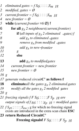
Available online: https://edupediapublications.org/journals/index.php/IJR/ P a g e | 45 ought to be eliminated and modified respectively in the reduced circuit C’. Initially eliminated gates is set to all the scan cells whereas the modified gates is void (lines 1-2). The circuit is traversed in breadth first searchorder using two lists current frontier and new frontier. While current frontier is set initially to all the scan cells of C (line 3), the new frontier initially is void (line 4). In the inner loop (lines 6-13) for all the gates neighbours of the current frontier it is checked where input gates already belong to eliminated gates (i.e. depend on scan cells). If this is the case then the currently evaluated gate is introduced into
eliminated gates, removed from modified gates (if applicable) and introduced to new frontier.[15] If at least one input does not belong to eliminated gates then the currently evaluated gate is introduced to
modified gates. In the outer loop (lines 5-16) while current frontier is not void (i.e. no more gates need to be eliminated) the inner loop proceeds further. At the end of each iteration of the outer loop current frontier and new frontier are updated (lines 14 and 15). Finally, using the eliminated gates and modified gates the initial circuit C is modified to the reduced circuit C’ (lines 16 and 17) as follows: gates that belong to eliminated gates (depend only on scan cells) are excluded; gates that belong to modified gates
(depend on both scan cells and primary inputs) are modified to gates with input signals dependent only on primary inputs (in the case of gates with two inputs of which one is a freezing signal, the gate is modified to a buffer);[16] all the freezing signals identified in the first step are set as primary outputs in the reduced circuit. Freezing signals f F S0; : : : ;F Sp 1g, which are the outputs of the gates present in the modified gates, are determined simultaneously with identifying independent scan cells (Definition 5). The independent scan cells are grouped into the extra scan chain (ESC) which consists of scan cells whose spurious transitions cannot be eliminated by computing an extra test vector. The algorithm returns not only the reduced circuit C’ but also the list of freezing signals that will be used in the following part of the MSC-PARTITIONINGof Figure 9.
Reduce
a
initial circuit C to
reduced circuit C’
Specify fault list L
for C’
b
ATPG for C’ using
fault list L; derive
c
extra test vectors
Available online: https://edupediapublications.org/journals/index.php/IJR/ P a g e | 46
in C using fault
L for C’
d
compatibility from C’
e
Generate multiple
scan chains based on
classification
self-incompatible
Yes
scan cells?
No
Scan chains {SC
0
, ... , SC
k-1
, ESC}
Extra Test Set ES = {EV , ... , EV
}
0 k-1
Available online: https://edupediapublications.org/journals/index.php/IJR/ P a g e | 47 In the second part a specified fault list L is created which will be provided together with the reduced circuitC’ to an ATPG tool. Specified fault listL comprises freezing signals F Si targeting the stuck-at the
non-controlling value sa nci of the gate gi from modified gates list of algorithm CIRCUIT-REDUCTION of Figure 10. It is important to note that each fault F Si sa nci has attached a list of scan cells f Si0 ; : : : ;Sim 1 g whose spurious transitions in the initial circuit C are eliminated when setting gateF Si to its controlling value. The list of scan cells is required during generation of scan chains in part d() of the MSC-PARTITIONING algorithm.[17]
In the third part, having generated the reduced circuitC’ and the specified fault list L, any state of the art
combinational ATPG tool can be used to generate test vectors for the faults fromL for C’. Test vectors for the faults fromL are the extra test vectors required to eliminate spurious transitions while shifting test responses in the initial circuitC as described in partd(). Since the freezing signals are primary outputs inC’ as described in parta() then L contains faults only on primary outputs. This will clearly speed up the ATPG process since only backward justification and no forward propagation is required. Moreover, the specified fault list is significantly smaller than the entire fault set which will further reduce ATPG computational time for computing extra test vectors. It should be noted that some faults fromL are redundant which implies that no extra test vector can be computed to stop the propagation of the spurious transitions from scan cells associated with the respective fault.[18] However, this scan cells are treated as self-incompatible and handled by re-specifying the fault list as described in the last parte)of( the MSC-PARTITIONING of Figure 4.9.
Given the extra test set with a list of faults from L detected by each extra test vector EVi, scan cell
classification according to definitions is done as follows. If two faults F Si sa nci and F S j sa nc j from L are incompatible (i.e. they are not detected by the same extra test vector) then each element of the two lists of scan cells associated with the two faults f Si0 ; : : : ;Sim 1 g and f S j0 ; : : : ;S jq 1 g respectively, are incompatible (otherwise they are compatible). This leads to grouping all the scan cells, associated with faults detectable by single extra test vector, into a single scan chain. However, this may lead to self-incompatible scan cells (Definition 4) when different extra test vectors eliminate spurious transitions from the same scan cell. Consequently, while there are self-incompatible the MSC-PARTITIONING algorithm will iterate through parts (e), (c), (d) as explained next.
ALGORITHM: CIRCUIT-REDUCTION
INPUT: CircuitC
OUTPUT: Reduced CircuitC’
Available online: https://edupediapublications.org/journals/index.php/IJR/ P a g e | 48
1
eliminated gates = f S
0
; : : : ;
S
m 1
g
2
modified gates = Ø
3
current frontier = f S
0
; : : : ;
S
m 1
g
4
new frontier = Ø
5
while (
current frontier
=
6
Ø) f
6
for all
g
x
2 neighbours(current frontier)
7
if (
all inputs of g
x
2 eliminated
gates) f
8
add g
xto eliminated
gates
9
remove g
xfrom modified
gates
10
add g
x
to new
frontier
11
g
12
else
13
add
g
x
to modified
gates
14
current frontier = new frontier
15
new frontier = Ø
16
g
17
generate reduced circuit
C’ as follows f
18
eliminate
all the gates g
x
2 eliminated gates
19
modify all the gates g
y2 modified gates
20
g
21
freezing signals f F S
0
; : : : ;
F S
p 1
g are
output signals of f g
0; : : : ;
g
p 1g = modified
gates
22
f S
e
0; : : : ;
S
e
m1g for which no freezing signal
exists are introduced in the extra scan chain
ESC
23
return Reduced CircuitC’
Freezing signalsf
F S
0
; : : : ;
F S
p 1
g
Figure 10: Proposed algorithm for circuit reduction for extra test vector computation
In the case that there are self-incompatible scan cells after the generation of multiple scan chains then the problem needs to be addressed as it was briefly explained in example 4. The faults F Si sa nci which have attached self-incompatible scan cells are removed from fault list L and new faults are specified on the lines in the fan out paths ofF Si. Thus, the respecified fault list L will be provided back to the ATPG process for computing extra test vectors (partc))which( will be followed by new multiple scan chain generation based on fault compatibility (part (d)). This iterative process continues until there are no self-incompatible scan cells left.
Available online: https://edupediapublications.org/journals/index.php/IJR/ P a g e | 49 chains and extra test vectors are computed without any knowledge of the test set to be applied to achieve the required fault coverage.[19] Therefore, computational time for circuit reduction depends only on the circuit size and structure (number of scan cells and circuit depth) and not on the size of the test set, which makes the proposed solution test set independent and applicable to large scan sequential circuits within low computational time. This is also due to the fact that although ATPG, used for detecting compatible faults in the reduced circuit, is NP-hard, efficient heuristics have been developed that could easily be integrated in the MSC-PARTITIONING algorithm. Note that the low computational time for large scan sequential circuits is achieved with small overhead in test area and test data which is also dependent only on the number of scan chains determined by the proposed MSC-PARTITIONING algorithm.
New Test Application Strategy Using Multiple Scan Chains and Extra Test Vectors
Having partitioned the scan cells into multiple scan chains with an extra test vector for each scan chain, this section introduces a new test application strategy for power minimisation during test application in scan sequential circuits. Node transition count NTC = å NG fi Cload is used as quantitative measure for
power dissipationthroughout the section. NG is the total number of gate output transitions (0 ! 1 and 1 ! 0)
and it is assumed that load capacitance for each gate is equal to the number of fan outs (Equation 1).
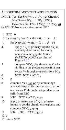
Multiple Scan Chain Test Application (MSC-TEST APPLICATION) algorithm computes the NT C during the entire test application period for the given test set S, circuit C, multiple scan chains f SC0; : : : ;SCk
1;ESCg, and extra test set ES = f EV0; : : : ;EVk 1g. Figure 11 gives the pseudo code of the proposed MSC-TEST APPLICATION algorithm. The value of NTC is 0 at the beginning of the algorithm and it is gradually increased as the entire test set is traversed. The outer loop represents the traversal of all the test vectors Vi, with i = 0; : : : ;n 1, from test set S. Shifting out test responses through all the scan chains are
then considered in the inner loop. For each scan chain SCj , circuit C is simulated by applying the extra
test vector EVj to primary inputs and NT Ci;j is added to NTC . NT Ci;j stands for node transition count
while shifting in present state part of test vector Vi through scan chain SCj and applying extra test vector EVj to the primary inputs. After shifting out the test responses though each scan chain SCj the primary
input part of test vector Vi is applied to primary inputs and NT Ci;E SC is computed while shifting out test
response through the extra scan chain ESC. Finally the entire test vector Vi
is applied to the circuit under test and NT Ci;LOADrequired to load the test response in the scan cells, is
Available online: https://edupediapublications.org/journals/index.php/IJR/ P a g e | 50
ALGORITHM: MSC-TEST APPLICATION
INPUT: Test Set S=f
V
0
; : : : ;
V
n
1
g
, Circuit C
Scan Chains f SC0; : : : ;SCk 1;ESCgExtra Test Set ES = f
EV
0
; : : : ;
EV
k
1
g
OUTPUT: Node transition count NTC
1 NTC 0
2
for every
V
i
from S with
i
=
0
; : : : ;
n
1 f
3
for every
SC
j
with
j
=
0
; : : : ;
k
1 f
4
apply
EV
j
to primary inputs;
EV
j
is
uniquely determined for
every
scan chain
SC
j
by the
MSC-PARTITIONING
algorithm of
Figure
4.10
5
compute
NT C
i;j
by simulating C when
shifting in the present state part of test
vector
V
i
through scan cells from
SC
j
6
NTC NTC
+
NT C
i;j7
g
8
compute
NT C
i;E SC
by simulating C
when shifting in the present state part of
test vector
V
i
through independent scan
cells from ESC
9
NTC NTC
+
NT C
i;E SC
10
apply primary part of
V
i
to primary
inputs to get the circuit test response and
compute
NT C
i;LOAD
11
NTC NTC
+
NT C
i;LOAD12
g
13
return NTC
Figure 11: Proposed test application strategy using multiple scan chains and extra test
Available online: https://edupediapublications.org/journals/index.php/IJR/ P a g e | 51
Experimental Results
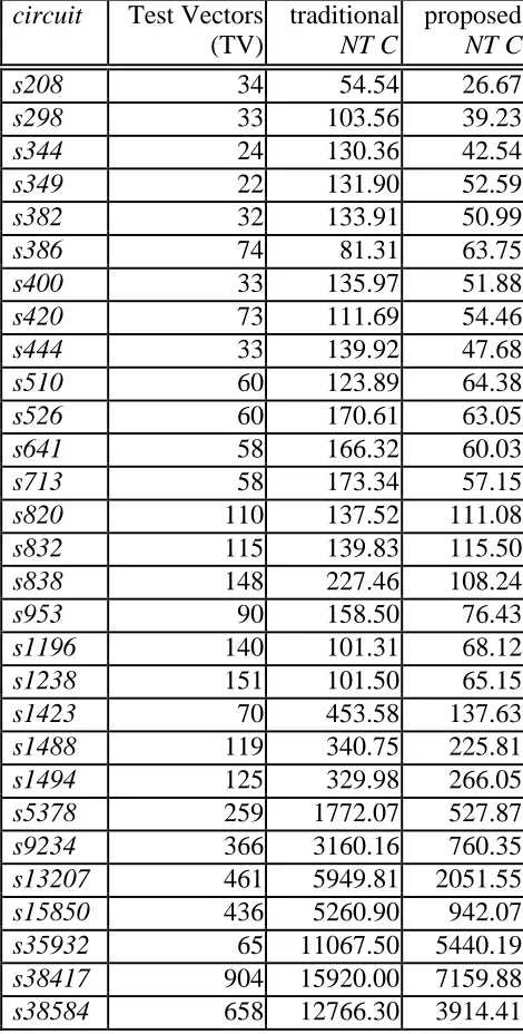
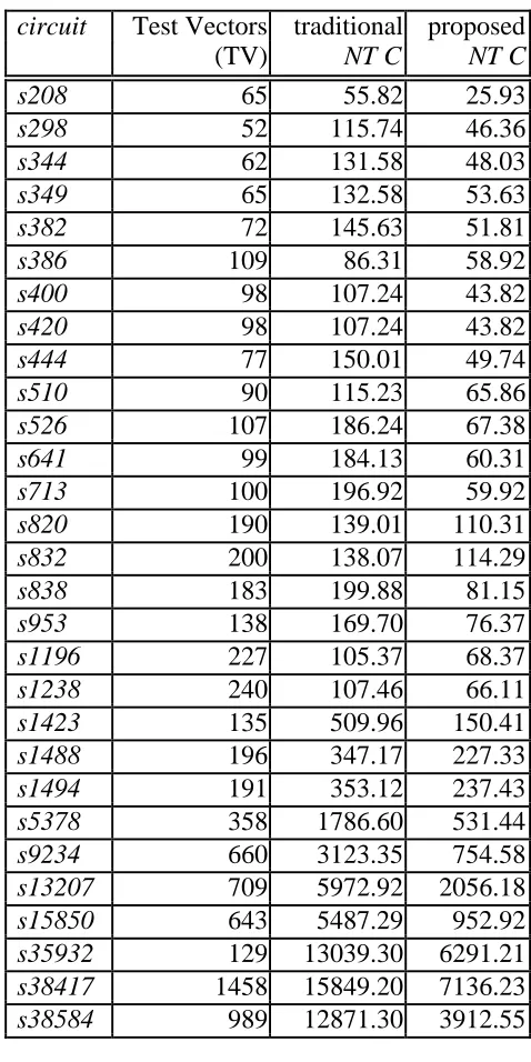
This section demonstrates through a set of benchmark examples that multiple scan chains combined with extra test vectors, as outlined in, yield savings in power dissipation during test application. The algorithms described in Section 4 were implemented on a 500 MHz Pentium III PC with 128 MB RAM running Linux and using GNU cc version. Shows the reduction in power dissipation at the expense of low overhead in test area and volume of test data, when the proposed multiple scan chains-based technique is employed for power minimisation. It provides a comparison with the BPIC test application strategy presented.
Experimental Results for Multiple Scan Chains-Based Power Minimisation
The average value of NT C reported throughout this section is calculated using the Equation 1 from under the assumption of the zero delay model. The use of the zero delay model is motivated by the observation that power dissipation under the zero delay model has a high correlation with power dissipation under the real delay model. Furthermore, due to elimination of spurious transitions the propagation of hazards and glitches is also eliminated leading to even greater reductions for power dissipation in the case of real delay model, as explained.
First column of Table 1 gives the number of scan cells of all full scan sequential circuits from ISCAS89 benchmark set. Second and third columns give the number of scan chains (SC) and the length of the extra scan chain (ESC) respectively computed using the MSC-PARTITIONING algorithm outlined. The number of scan chains varies from 2 as in the case of s208 up to 7 as in the case of s38584. The small
Available online: https://edupediapublications.org/journals/index.php/IJR/ P a g e | 52
circuit
Scan
Scan
ESC
CPU
Cells Chains (SC) length time (s)
s208
8
2
0
1
s298
14
3
6
1
s344
15
4
4
1
s349
15
4
1
1
s382
21
3
6
1
s386
6
3
0
1
s400
21
3
6
1
s420
16
2
0
1
s444
21
4
6
1
s510
6
4
0
1
s526
21
4
6
1
s641
19
3
0
1
s713
19
3
0
1
s820
5
5
0
1
s832
5
3
0
1
s838
32
2
0
1
s953
29
3
23
1
s1196
18
4
2
1
s1238
18
4
2
1
s1423
74
5
3
2
s1488
6
3
0
3
s1494
6
4
0
3
s5378
179
5
33
49
s9234
211
6
20
201
s13207
638
5
330
472
s15850
534
6
62
596
s35932
1728
2
0
1903
s38417
1636
5
1079
8151
s38584
1426
7
7
3543
Table 1: Experimental results for ISCAS89 benchmark circuits in terms of number of scan
chains, extra scan chain (ESC) length, and CPU time, when applying
MSC-PARTITIONING
Available online: https://edupediapublications.org/journals/index.php/IJR/ P a g e | 53
circuit
Test Vectors traditional proposed
(TV)
NT C
NT C
s208
34
54.54
26.67
s298
33
103.56
39.23
s344
24
130.36
42.54
s349
22
131.90
52.59
s382
32
133.91
50.99
s386
74
81.31
63.75
s400
33
135.97
51.88
s420
73
111.69
54.46
s444
33
139.92
47.68
s510
60
123.89
64.38
s526
60
170.61
63.05
s641
58
166.32
60.03
s713
58
173.34
57.15
s820
110
137.52
111.08
s832
115
139.83
115.50
s838
148
227.46
108.24
s953
90
158.50
76.43
s1196
140
101.31
68.12
s1238
151
101.50
65.15
s1423
70
453.58
137.63
s1488
119
340.75
225.81
s1494
125
329.98
266.05
s5378
259
1772.07
527.87
s9234
366
3160.16
760.35
s13207
461
5949.81
2051.55
s15850
436
5260.90
942.07
s35932
65
11067.50
5440.19
s38417
904
15920.00
7159.88
s38584
658
12766.30
3914.41
(a) ATALANTA test set
Table 2: Comparison in
NT C
when using the proposed multiple scan chains and the traditional
single scan chain
Available online: https://edupediapublications.org/journals/index.php/IJR/ P a g e | 54
circuit
Test Vectors traditional proposed
(TV)
NT C
NT C
s208
65
55.82
25.93
s298
52
115.74
46.36
s344
62
131.58
48.03
s349
65
132.58
53.63
s382
72
145.63
51.81
s386
109
86.31
58.92
s400
98
107.24
43.82
s420
98
107.24
43.82
s444
77
150.01
49.74
s510
90
115.23
65.86
s526
107
186.24
67.38
s641
99
184.13
60.31
s713
100
196.92
59.92
s820
190
139.01
110.31
s832
200
138.07
114.29
s838
183
199.88
81.15
s953
138
169.70
76.37
s1196
227
105.37
68.37
s1238
240
107.46
66.11
s1423
135
509.96
150.41
s1488
196
347.17
227.33
s1494
191
353.12
237.43
s5378
358
1786.60
531.44
s9234
660
3123.35
754.58
s13207
709
5972.92
2056.18
s15850
643
5487.29
952.92
s35932
129
13039.30
6291.21
s38417
1458
15849.20
7136.23
s38584
989
12871.30
3912.55
(b) ATOM test set
Table 3: Comparison in
NT C
when using the proposed multiple scan chains and the traditional
single scan chain
value of NT C (traditional NT C), which is the total value of NT C using the traditional single scan chain design [2] and ALAP test application strategy (Definition 3 in Chapter 3) divided by the total number of clock cycles over the entire test application period. The next column 4 shows the final average value of
Available online: https://edupediapublications.org/journals/index.php/IJR/ P a g e | 55