ISSN(Online): 2320-9801
ISSN (Print): 2320-9798
I
nternational
J
ournal of
I
nnovative
R
esearch in
C
omputer
and
C
ommunication
E
ngineering
(A High Impact Factor, Monthly, Peer Reviewed Journal) Website: www.ijircce.com
Vol. 7, Issue 5, May 2019
Low Power and High Performance Shift
Registers Using Pulsed Latch Technique
Jacob B Cacko, Gajendra Sujediya
Assistant Professor, RIET Jaipur, Rajasthna, India
Research Scholar, RIET Jaipur, Rajasthna, India
ABSTRACT: This work presents an elegant methodology using pulsed latch instead of flip-flop without altering the
existing design style. Pulsed-latch technique retain the advantages of both latches and flip-flops and thus one can achieve both high speed and lower power consumption simultaneously. In this work, pulsed latch technique has been used to reduce the delay of various shift registers without increasing any power consumption. In very high speed VLSI circuits due to heavy pipelining there is requirement of low power edge triggered flip-flops. However, for low power consumption in these very high speed VLSI circuits, the migration from flip-flop to pulsed latch technique has become a great success. In the proposed work, non-overlapped delayed pulse clock has been used in pulse latch technique to eliminate the timing problem between the pulsed latches. All the proposed shift registers have been designed in 180 nm CMOS technology and their functionality have been verified using Cadence Virtuoso. From this work, it has been concluded that, the pulse latch technique reduces the power consumption significantly in the designed registers and overall there is an improvement in power delay product. Further, it is pertinent to mention that the proposed registers require less number of transistors for their implementation as compared to conventional versions.
I. INTRODUCTION
Recently, many methodologies have been introduced for reducing dynamic power for systems – on - chip (SoCs). These methodologies, however, impose restrictive physical constraints which have schedule impact or which are heavily dependent on logic functions such as clock gating. Dynamic power is consumed across all elements of a chip. The clock network is one of the large consumers of dynamic power. Therefore, reducing power in the clock network can impact the overall dynamic power significantly. Designers already use a variety of techniques to reduce the clock power using smaller clock buffers, reducing the overall wiring capacitance, employing clock gating to reduce the dynamic power, and de cloning to move the clock buffers at higher levels of hierarchy. Even with these techniques, the dynamic power of clock network can be large since registers are used as state elements in the design. In general, a flip - flop is used as the register or you can say sequential circuits
II. PULSED LATCH CONCEPT
ISSN(Online): 2320-9801
ISSN (Print): 2320-9798
I
nternational
J
ournal of
I
nnovative
R
esearch in
C
omputer
and
C
ommunication
E
ngineering
(A High Impact Factor, Monthly, Peer Reviewed Journal) Website: www.ijircce.com
Vol. 7, Issue 5, May 2019
1. Clock energy
2. Data energy
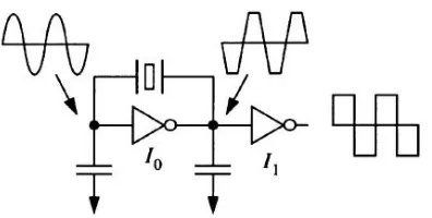
Oscillator Circuit for Clock Generation
Some chips contain on-chip clock generation circuits using crystal oscillator devices. The simplest oscillator circuit is shown in Figure 1 ,The inverter I0 serves as a gain amplifier for the feedback oscillator and the inverter I1 reshape the waveform to obtain a proper digital clock signal. To minimize power dissipation of tcircuit, several trade-off decisions have to be considered. For good stability of oscillation, we like to set a large gain on the inverter I0, However, a large gain results in large voltage swing and short-circuit current that increase the power dissipation. Thus, it is important to tune the transistor sizes of the inverters to achieve a proper trade-off between the "quality" of oscillation and the power dissipation of the circuit.
Fig. 1 An on-chip crystal oscillator circuit
PULSED LATCH ISSUES AND OPTIMIZATION
ISSN(Online): 2320-9801
ISSN (Print): 2320-9798
I
nternational
J
ournal of
I
nnovative
R
esearch in
C
omputer
and
C
ommunication
E
ngineering
(A High Impact Factor, Monthly, Peer Reviewed Journal) Website: www.ijircce.com
Vol. 7, Issue 5, May 2019
III. PROPOSED APPLICATIONS OF PULSED LATCH
There are wide range of applications for pulsed latches. Pulsed latches could be used in portable devices where low power consumptions is necessary like the applications where flip-flops could be replaced with pulse latches i.e. in pipelining or as sequencing element or as register.
Shift Registers
A sequential logic block made up of flip-flops that allows parallel or serial loading and series or parallel outputs as well as shifting bit-by-bit is called Shift Register. It is the basic building block in a VLSI circuit. They are commonly used in many applications, such as digital filters, communication receivers, and image processing ICs. Recently, as the size of the image data continues to increase due to the high demand for high quality image data, the word length of the shifter register increases to process large image data in image processing ICs. An image-extraction and vector generation VLSI chip uses a 4K-bit shift register. A 10-bit 208 channel output LCD column driver IC uses a 2K-bit shift register. A 16-megapixel CMOS image sensor uses a 45K-bit shift register. The area and power consumption of the shift register become important design considerations as the word length of the shifter register increases.
IV. SIMULATION RESULTS
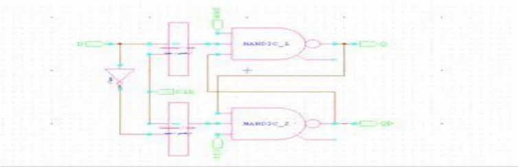
Figure shows the schematic of D flip-flop and figure 6.2 working of flip-flop can be verified by waveform. Output follows the input and first waveform provides average power dissipation in flip-flop.
ISSN(Online): 2320-9801
ISSN (Print): 2320-9798
I
nternational
J
ournal of
I
nnovative
R
esearch in
C
omputer
and
C
ommunication
E
ngineering
(A High Impact Factor, Monthly, Peer Reviewed Journal) Website: www.ijircce.com
Vol. 7, Issue 5, May 2019
Fig. 4 D flip-flop using NAND gate waveform
V. CONCLUSIONS
The requirement of replacement element for flip-flops in recent trend, led to migration from flip-flops to the pulsed latch for low power consumption, less area and delay applications. In this thesis, we have proposed different applications of pulsed latch using 180nm technology in Tanner tool v 14.1 and performance is compared with application using flip-flop. The number of transistors utilized in pulsed latch is less than that of flip-flop, hence area is significantly reduced. Pulsed latch circuit saves power consumption and power delay product in comparison with flop circuit hence it can be inferred from the results that the circuits using the pulsed latches can be used instead of flip-flop for low power, less area and high speed applications. It also eliminates one latch per cycle and doesn’t require clock complement. Other advantages include minimised sequencing overhead, easier timing verification, lower delay and time borrowing capability. The trading towards applications using pulsed latches from conventional flip-flop circuits in heavy pipelining, mobile devices or in low power ASIC circuits is immense achievement in field of VLSI designing.
REFERENCES
[1] S. Shibatani, A. H. C. li, “Pulse latch approach reduce dynamic power”, EE times online, 2016.
[2] P. Reyes, P. Reviriego, J. A. Maestro, and O. Ruano, “New protection techniques against SEUs for moving average filters in a radiation
ISSN(Online): 2320-9801
ISSN (Print): 2320-9798
I
nternational
J
ournal of
I
nnovative
R
esearch in
C
omputer
and
C
ommunication
E
ngineering
(A High Impact Factor, Monthly, Peer Reviewed Journal) Website: www.ijircce.com
Vol. 7, Issue 5, May 2019
[5] H. Lee, S. Paik, and Y. Shin, “Pulse width allocation with clock skew scheduling for optimizing pulsed latch-based sequential circuits” IEEE
International conference onComputer-aided design, pp. 224-229, July 2018.
[6] R. Kumar, K. Bollapalli , and S. Khatri, “A robust pulsed flip-flop and its use in enhanced scan design,” IEEE International Conference on Computer Design, pp. 97-102, Oct. 2009.