ABSTRACT
JACKSON, SHANNON MARIE. Microstructure-Property Studies of
Sputter Deposited Cu1-x Tax Thin Films. (Under the direction of Dr. J.M. Rigsbee.)
A series of Cu1-xTax (x = 0.05 to 0.5) thin films have been produced by DC
magnetron sputter deposition using co-deposition (alloy) and sequential (layered)
deposition modes at ambient temperature. The nanoscale microstructures of these
non-equilibrium “alloy” films have been investigated chemically and structurally using x-ray
diffraction, scanning electron microscopy and high-resolution transmission electron
microscopy. The mechanical properties were measured via nanotriboligical and
nanoindentation studies of selected samples to determine the affect of Ta composition
and nanolayer thickness.
XRD indicated that the Cu was deposited with a (111) texture and the Ta texture
differed with percent Ta for the co-deposited alloy films and was dependent on thickness
for the nanolaminate thin films. As the percent Ta increased for the alloy films, the
structure of the film changed from a randomly-oriented β Ta texture to a highly-textured
(002) oriented β Ta. The highly-textured (002) oriented β Ta became more prevalent as
the layer thickness decreased from ~7 nm to ~3.5 nm for the nanolaminate films.
Nanotribological and nanoindentation studies of the mechanical properties of the
films showed that the nanolaminate films possessed a higher scratch resistance and
exhibited higher elastic modulus and hardness values.
Nanolayer deposition was achieved via a rotating fixture that allowed for
MICROSTRUCTURE-PROPERTY STUDIES OF
SPUTTER DEPOSITED Cu
1-xTa
xTHIN FILMS
by
Shannon Marie Jackson
A thesis submitted to the Graduate Faculty of North Carolina State University
in partial fulfillment of the requirements for the Degree of
Master of Science
MATERIALS SCIENCE AND ENGINEERING
Raleigh, NC
May 2007
APPROVED BY:
________________________________ _________________________________ Dr. Afsaneh Rabiei Dr. Zlatko Sitar
________________________________ Dr. J.M. Rigsbee
DEDICATION
Dedicated to my husband,
Robert Belz,
BIOGRAPHY
Shannon Marie Jackson was born in Charleston, SC on May 9, 1979 to Robert and Teresa
Jackson. She also has a younger brother, Shaun Jackson. Shannon grew up in
Summerville, SC. Attending Summerville High School, Shannon excelled in science and
math. Shannon was president of Summerville High School’s Junior Academy of Science
her sophomore year, and president of her church youth group her junior and senior year.
After high school, she was accepted into the College of Charleston in Charleston, SC
majoring in Chemistry. As a result of an inspiring internship in the Materials and
Chemical Laboratory at the Robert Bosch Corporation in North Charleston, SC, Shannon
focused her studies on Materials Science and Engineering. After completing the first half
of the 3-2 Engineering program at College of Charleston, Shannon transferred to the
Materials Science and Engineering department at North Carolina State University. She
served as the Materials Technical Society president at NCSU her final year, earning her
the Materials Leadership Scholarship and was also awarded the Society of Plastic
Engineers Senior Award Scholarship. After achieving a Bachelor of Science in Materials
Science and Engineering from NCSU and a Bachelor of Science in Physics from the
College of Charleston, she chose to continue her education in Materials Science and
Engineering under the direction of Dr. J. M. Rigsbee with her research interest in sputter
deposition of thin films. She received her Master of Science in May 2007 and is
ACKNOWLEDGEMENTS
I would like to sincerely thank my advisor Dr. J. Michael Rigsbee for his
guidance, patience, and encouragement during my research work. I would like to thank
Dr. Zlatko Sitar and Dr. Afsaneh Rabiei for not only serving on my thesis committee, but
also as excellent professors with contagious enthusiasm for teaching. I would like to
express my gratitude to all the professors in the Materials Science and Engineering
department who inspire and challenge young engineers to achieve their goals.
A special thanks to Dr. Jag Kasichainula for assisting and working with the
Center for Tribology, Inc. to provide tribological testing, Mr. Mark Koopman at the
University of Alabama at Birmingham for performing the nanoindentation testing and
assistance in interpretation of the results, Mr. Alex Kvit for aiding in the preparation and
analysis of the TEM samples.
I would also like to thank Mr. Marcus Hunt, Mrs. Candice Lundy, Mr. Brian
Laughlin, Mr. Jon Ihlefeld, and Mr. Tai-Nan Lin for your support and knowledge sharing
whenever I needed a few extra brain cells! And all my friends in CAMP-M, who could
always be counted on for lunch breaks. Ms. Edna Deas - there are not enough words to
express my gratitude for the support you have provided – you are the rock in the
Materials Science and Engineering department.
And finally, none of this would have been possible without the support from my
family and friends. Your continual encouragement has made me the person I am today
TABLE OF CONTENTS
LIST OF TABLES ... vi
LIST OF FIGURES ... vii
1 INTRODUCTION... 1
1.1 Why Copper and Tantalum? ... 1
1.1.1 Copper... 1
1.1.2 Tantalum... 2
1.1.3 Copper and Tantalum “Alloys”... 4
1.2 Phenomenon of Sputtering... 6
1.2.1 Magnetron Sputtering... 9
1.3 Nanolaminates... 11
1.4 Transmission Electron Microscopy ... 13
1.5 Nanoindentation... 15
1.5.1 Berkovich Indenter... 16
2 EXPERIMENTAL METHOD... 19
2.1 Film Deposition ... 19
2.1.1 Denton Discovery 18 ® Magnetron Sputtering System... 20
2.1.2 Alloyed Thin Films... 22
2.1.3 Determination of Deposition Rate of “Alloyed” Films... 24
2.1.4 Nanolaminate Thin Films... 26
2.1.5 Determination of Deposition Rate of Nanolaminate Films... 30
2.2 Materials Characterization ... 32
2.2.1 X-ray Diffraction (XRD)... 32
2.2.2 Scanning Electron Microscopy... 32
2.2.3 Transmission Electron Microscopy... 33
2.2.4 Nanotribology... 33
2.2.5 Nanoindentation... 36
3 RESULTS AND DISCUSSION ... 39
3.1 Profilometry ... 39
3.2 Scanning Electron Microscopy (SEM) ... 40
3.3 Transmission Electron Microscopy ... 44
3.4 X-Ray Diffraction (XRD) ... 50
3.5 Nanotribology ... 57
3.5.1 Coefficient of Friction (COF)... 57
3.5.2 Scratch Resistance... 61
3.6 Nanoindentation... 64
4 CONCLUSIONS AND FUTURE WORK ... 72
4.1 Conclusions... 72
4.2 Future Work... 74
LIST OF TABLES
Table 1.1: Property comparison of refractory metals... 3
Table 1.2: Thermal and mechanical properties of α and β tantalum8... 4
Table 1.3: Geometrical relationships and constants for the Berkovich indenter... 18
Table 2.1: Alloy thin film trial parameters... 24
Table 2.2: Film thickness as a function of cathode power and location on substrate (T-B is the difference between the top and bottom)... 27
Table 2.3: Calculated layer thickness for Cu and Ta as a function of cathode power and platen RPM... 29
Table 3.1: Profilometry data for nanolaminate thin films... 40
Table 3.2: Quantitative EDS data of alloyed thin films... 41
Table 3.3: EDS analysis of trials C2 and D2 with new Cu cathode to substrate distance43 Table 3.4: Trial parameters in attempt to produce 50%Cu/50%Ta alloy film and quantitative EDS results... 43
Table 3.5: Predicted versus measured layer thickness for Trial 2... 45
Table 3.6: Coefficient of Friction (COF) and Root Mean Square (RMS) values of samples ... 57
Table 3.7: Critical load results for the scratch resistance testing... 61
Table 3.8: Summary of nanoindentation results for the thin films... 70
LIST OF FIGURES
Figure 1.1: Calculated Cu-Ta phase diagram based on limited data by Verhoeven11... 5
Figure 1.2: Variation in sputter yield with respect to the incident ion energy 16... 8
Figure 1.3: Schematic of a typical DC sputtering system... 8
Figure 1.4: Planar-magnetron structure and behavior17... 10
Figure 1.5: Schematic diagram and composition profiles for a multilayered material2212 Figure 1.6: Geometry of Berkovich indenter forms upon contact... 17
Figure 1.7: Indentation made by Berkovich indenter 29... 17
Figure 2.1: Denton Discovery 18 (R) Magnetron Sputter Deposition System... 21
Figure 2.2: Schematic of the confocally-mounted cathode arrangement... 22
Figure 2.3: Deposition rate versus power for copper deposition... 25
Figure 2.4: Deposition rate versus power for tantalum deposition... 25
Figure 2.5: 3-D model of the fixture used in the nanolaminate film deposition. Also indicates placement of the substrates.... 27
Figure 2.6: Image of the fixture used for this research after attached to the platen... 28
Figure 2.7: CAD diagram indicating the dimensions of the fixture.... 29
Figure 2.8: Deposition rate versus power of copper for nanolaminate deposition... 30
Figure 2.9: Deposition Rate versus Power of tantalum for nanolaminate deposition.... 31
Figure 2.10: Schematic of friction test set-up for coatings (CETR) 33... 34
Figure 2.11: Schematic of scratch test for thin film coatings (CETR) 33... 35
Figure 2.12: MTS Nanoindenter XP system34... 36
Figure 3.1: Deposition Rate for initial distance and increased Cu target distance... 42
Figure 3.2: Low magnification TEM micrograph of the nanolaminate film... 45
Figure 3.3: TEM micrograph of the nanolaminate film on the Si substrate showing approximate layer thickness of 7.0 nm for Cu and 8.5 nm for Ta.... 46
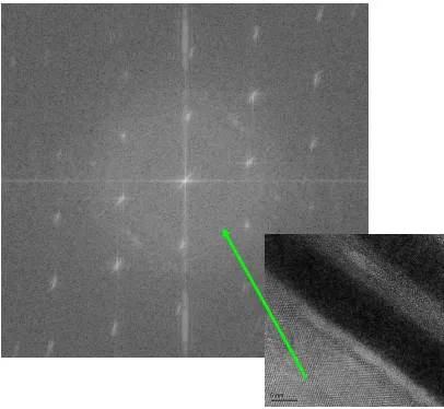
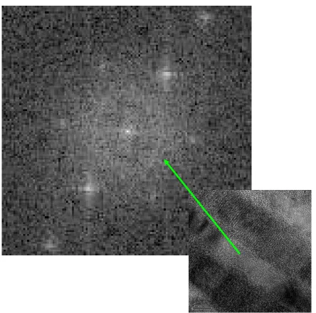
Figure 3.4: FFT of the Si substrate. The image used is shown in the bottom right and the diffractogram was obtained from the Si substrate indicated by the green arrow.... 47
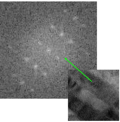
Figure 3.5: FFT of the Ta layer substrate. The HRTEM image used is shown in the bottom right and the diffractogram was obtained from the light area on the BF image, predicted Ta, indicated by the green arrow.... 48
Figure 3.6: FFT of the Cu layer substrate. The HRTEM image used is shown in the bottom right and the diffractogram was obtained from the darker area on the BF image, predicted Cu, indicated by the green arrow.... 49
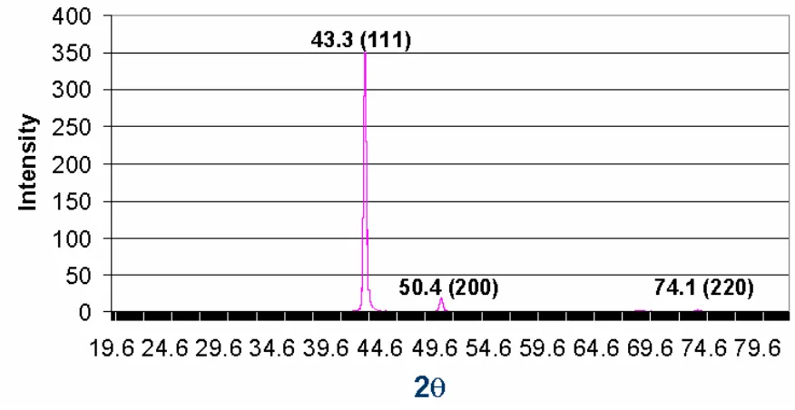
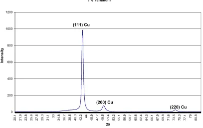
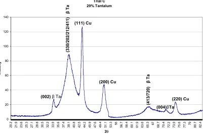
Figure 3.7: Intensity as a function of diffraction angle for as-deposited Cu... 50
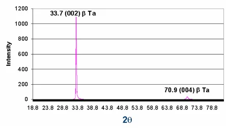
Figure 3.8: Intensity as a function of diffraction angle for as-deposited Ta... 51
Figure 3.9: Intensity as a function of diffraction angle for Trial A... 52
Figure 3.10: Intensity as a function of diffraction angle for Trial B.... 53
Figure 3.11: Intensity as a function of diffraction angle for Trial C... 53
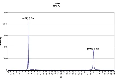
Figure 3.12: Intensity as a function of diffraction angle for Trial D... 54
Figure 3.13: Intensity as a function of diffraction angle for Trial 2 (5 RPM)... 55
Figure 3.14: Intensity as a function of diffraction angle for Trial 3 (10 RPM)... 56
Figure 3.15: Coefficient of Friction data for Trial C, Run 1 (red) and Run 2 (green).... 58
Figure 3.16: Coefficient of Friction data for Trial F, Run 1(red) and Run 2(green)... 58
Figure 3.18: Coefficient of Friction data for nanolaminate Trial 3... 60
Figure 3.19: Scratch resistance data for Trial C... 62
Figure 3.20: Scratch resistance data for Trial F... 62
Figure 3.21: Scratch resistance data for Trial 2 sample... 63
Figure 3.22: Scratch resistance data for Trial 3 sample... 64
Figure 3.23: Micrograph of indentations made by the Berkovich indenter during the nanoindentation testing.... 65
Figure 3.24: Representative graph of Modulus vs. Indentation Depth for Copper film. 66 Figure 3.25: Representative graph of Modulus vs. Indentation Depth for Tantalum film ... 66
Figure 3.26: Representative graph of Modulus vs. Indentation Depth for Trial C... 67
Figure 3.27: Representative graph of Modulus vs. Indentation Depth for Trial G... 67
Figure 3.28: Representative graph of Modulus vs. Indentation Depth for Trial 1... 68
Figure 3.29: Representative graph of Modulus vs. Indentation Depth for Trial 2... 68
Figure 3.30: Representative graph of Modulus vs. Indentation Depth for Trial 3... 69
1 INTRODUCTION
Within the past decade, many once immiscible alloy systems have been developed via
physical vapor deposition techniques. Alloys consisting of copper and refractory metals (i.e.
Cr, W, Ta, Nb), which usually show virtually no mutual solubility in the liquid or solid
states, have been the focus of a number of these new systems. Studies of these
nonequilibrium and often nanocrystalline alloy systems were motivated by a need for
structural materials with high thermal conductivity and high strength at elevated temperatures
and diffusion barrier materials for microelectronic devices.
Several questions investigated during the scope of this research include:
What effect does Ta composition have on the mechanical properties of co-sputter-deposited Cu1-xTax (x = 0.05 to 0.5) alloy thin films?
How do the mechanical properties differ between the co-sputter deposited alloy thin films and the co-deposited nanolaminate films with varying layer thickness?
What is the microstructure of the as-deposited alloy and nanolaminate thin films?
Is an alternating nanolayer structure achievable via magnetron sputter deposition?
1.1 Why Copper and Tantalum?
1.1.1 Copper
Copper is the 29th element on the periodic chart with an atomic weight of 63.54
g/mol, density of 8.92 g/cm3 and a melting point of 1084°C1. The crystal structure of copper
is face centered cubic (FCC) and has a lattice parameter of 0.361 nm. The commercial
electrical contacts, heat exchangers and decorative finishes, as well as many other
applications. The widespread use of copper is due to its excellent electrical conductivity (58
x 106 S/m @ 20°C) and thermal conductivity (394 W/mK @ 20°C), outstanding resistance to
corrosion, ease of fabrication, and good strength and fatigue resistance2. Many copper
alloys, such as brass and bronze, are common materials that have been known for centuries,
in fact the use of copper dates back 10,000 years3.
The electronics industry has continued to develop new copper alloys to meet the
requirements of the advancing electronics technology2. The high thermal conductivity of
copper makes it desirable in many electronics applications to provide rapid conduction of
heat from a heat source such as for thermoelectric coolers.
The relatively low tensile (221 MPa) and yield strengths (69 MPa) of pure, fully
annealed, polycrystalline copper limit its use as a structural material2. Although extensive
cold working increases the tensile and yield strengths to 455 and 365 MPa2, respectively, the
low recrystallization temperature of copper limits its use to below 120°C for 99.999 wt%
Cu4. The addition of alloying elements by solid solution strengthening or precipitation
hardening will increase the working temperature and dramatically improve the mechanical
properties of copper. Conversely, they have a negative affect on the electrical and thermal
conductivity. Other concerns must also be taken into consideration with the addition of
alloying elements. For example, zinc can significantly increase the strength of copper, but it
also increases the risk of stress-corrosion cracking in certain environments2.
53rd most abundant element on the earth1. The crystal structure of tantalum is body centered
cubic (BCC) and has a lattice parameter of 0.330 nm. Tantalum is one of the denser
refractory metals at 16.6 g/cm3 and is second only to tungsten in melting temperature,
2996°C for Ta and 3410°C for W. Tantalum also exhibits excellent corrosion resistance and
workability. Table 1.1 compares several of the properties of the most common refractory
metals.
Table 1.1: Property comparison of refractory metals
Melting Point (ºC)
Density (g/cc)
Young's Modulus @ 20ºC (GPa)
Tensile Strength @ 20ºC (GPa)
Thermal Expansion
(ppm/ºC)
Thermal Conductivity
(W/cm-ºC)
Tantalum (Ta) 2996 16.6 185 0.2-0.5 6.3 0.52
Tungsten (W) 3410 19.3 410 0.7-3.5 4.5 1.70
Molybdenum (Mo) 2617 10.2 330 0.7-1.4 4.8 1.40
Niobium (Nb) 2468 8.6 130 0.4-0.7 7.3 0.54
Rhenium (Re) 3180 21 450 0.7-2.0 6.2 0.40
In 1965, Read and Altman6 discovered a new tantalum phase in sputtered tantalum
films, which they called β-tantalum. This phase was also found in evaporated and chemical
vapor deposited films. At that time, it was not apparent whether β-Ta was an allotrope of
BCC Ta or an impurity-stabilized tantalum phase6. The investigation into the structure of β
-tantalum is still continuing almost forty years later. More recently, Jiang et al.7 investigated
the proposed models for β-Ta which included a β-Uranium based structure, a distorted A15
structure, a bcc-Ta based superlattice structure with N interstitials, and a simple HCP
structure. This research indicated that the β-Uranium model was consistent with the
experimental data, therefore it was concluded that β-Ta has a tetragonal structure containing
30 atoms per unit cell with the space group P42/mnm7. This conclusion appears widely
Studies by Lee et al.8 showed that sputter deposited tantalum formed a high (002) β-
Ta texture at low sputter gas pressure (≤ 10 mTorr) and random-oriented β-Ta at higher gas
pressure. The properties of the α-Ta and β-Ta differ significantly. Table 1.2 is a comparison
of the thermal and mechanical properties of α and β-Ta.
Table 1.2: Thermal and mechanical properties of α and β tantalum8
Phase Alpha Ta Beta Ta
Structure BCC Tetragonal
Lattice Parameters a=b=c=0.330 nm a=b=1.1094 nm, c=0.5313 nm Hardness 200-400 KHN 1000-1300 KHN
Ductility Ductile Brittle
Resistivity 15-60 µΩ cm 170-210 µΩ cm
Thermal Stability Tmelting point at 2996°C Tβ- α at 750-775°C
The phase transformation temperature from β-Ta to α-Ta is dependent on the texture
of the film. A study by Lee et al. 8confirmed that the random (002) beta tantalum underwent
a phase transformation to α-Ta near 750°C, whereas the highly (002) textured beta tantalum
transformed near 300°C. Occasionally, a mixture of the beta tantalum and alpha tantalum
(BCC) are observed dependent on deposition technique and deposition parameters9.
1.1.3 Copper and Tantalum “Alloys”
The solid solubility of tantalum in copper is negligible based on experiments by
Verhoeven et al. and upon comparison with a similar system, Cu-Nb11. Thermodynamic
modeling of the limited data by Verhoeven produced the Cu-Ta phase diagram in shown in
Figure 1.1: Calculated Cu-Ta phase diagram based on limited data by Verhoeven11
Due to the limited mutual solid solubility of Cu and Ta, various techniques have been
attempted to create a non-equilibrium alloy. Previous research has shown ion implantation of
Ta into Cu thin films produced a metastable substitutional solid solution at low Ta
concentrations (~1 at. %)12. Cullis
et al.12 found that the Ta-Cu implanted alloys exhibited a
phase transformation from the metastable substitutional solid solution to a non-crystalline
structure at ~10% at% Ta. Nastasi et al. 13coevaporated amorphous films of a-CuxTa(1-x) (x
= 0.10 – 0.55) to study the crystallization temperature and effect of ion irradiation. They
found that the crystallization temperature of the a-CuxTa(1-x) film increased with increasing
(~13 DPA) did not affect the Cu10Ta90 or Cu20Ta80 films, but did promote phase separation of
FCC Cu and tetragonal Ta in copper-rich samples13.
Previous work with co-sputter-deposited Cu1-xTax alloys by Wang et al.14investigated
the crystal structure and morphology of the Ta particles as a function of deposition
temperature and the thermal stability of the Ta particle structure and distribution as a function
of Ta content and annealing. This work showed the possibility of creating nonequilibrium
alloys such as Cu-Ta utilizing sputter deposition. The substrate temperature was shown to
influence the level of Ta in solid solution with Cu, with Ta solubility increasing with
decreased temperature. The reduced temperature, in this case -120°C, limited the surface
diffusion thus trapping Ta in solid solution14. The fcc Ta and bcc Ta in the Cu0.94Ta0.06 and
Cu0.83Ta0.17 alloy films, respectively, did not demonstrate Ta particle coarsening after
annealing at 900°C for 100 hours14. Mechanical testing showed an increase in hardness of
about 3 times that of the Cu films, although, the strengthening mechanisms in each of films
varies based on the different microstructures14. Mechanical strength, as evaluated by
nanoindentation, was not reduced by the 900°C annealing treatments.
1.2 Phenomenon of Sputtering
Atom-by-atom deposition of materials can be completed by both physical and
chemical means, each having their advantages and disadvantages. The method of deposition
chosen is dependent on varying factors including, but not limited to, the material to be
deposited, the structure of the film, production volumes, financial resources, and available
deposition process of sputtering as a means of deposition, so this will be the focus of the
following discussion.
Sputtering is a physical process involving the removal of atoms from the surface and
near surface of a bulk piece by the bombardment of the surface with energetic ions15. The
sputter yield, S, defines the mean number of atoms removed from the surface of the target per
incident ion and is calculated as
atoms removed S
incident ions =
Typical sputtering yields range from 10-1 to 10, however ranges from 10-5 to 103 have
been obtained experimentally15. The energy of the incident ions significantly changes the
sputter yield. Typical ion energies range from a few to a hundred electron volts in typical
glow discharges, whereas; the typical energy for sputtered atoms ranges from 2 to 7 eV15.
There exists a low energy threshold for sputtering and also a maximum value at high
Figure 1.2: Variation in sputter yield with respect to the incident ion energy 16
DC sputtering is the oldest and simplest excitation method; however it is limited to
electrically conducting materials. For electrically insulating materials, RF excitation is used.
A typical DC sputtering system is shown schematically in Figure 1.3.
Cathode (Target)
Substrates
Anode
Vacuum Glow Discharge
DC sputtering is usually carried out at ambient temperature and at reduced pressures
(10 – 100 mTorr). The sputtering gas is most commonly argon because of its non-reactivity
and its medium atomic mass; however, other gases can be used. Due to the low deposition
rates and relatively high working pressures needed to sustain DC plasma, DC sputtering can
have high contamination levels and is rarely used15.
1.2.1 Magnetron Sputtering
Magnetron sputtering, because of its much higher deposition rates and lower working
pressures, is the most common variation of DC sputtering. Magnetron sputtering systems
add a permanent magnet to the cathode assembly. This configuration creates lines of
magnetic flux perpendicular to the electric field, and parallel to the surface of the target. The
magnetic field concentrates the plasma in the space directly in front of the target. This
increases ionization of the argon working gas by the effect of the magnetic field on the paths
of the electrons emitted from the cathode. The enhanced working gas ionization increases the
ion bombardment and sputtering rates. Sputtering, in all cases, is the result of momentum
transfer; however, due to the lower working pressures with magnetron sputtering, the
sputtered atoms are removed in a ‘ballistic fashion’15. Figure 1.4 depicts a typical planar
Figure 1.4: Planar-magnetron structure and behavior17
The disadvantage of magnetron sputtering is the decrease in life of the cathode target.
Due to the ions being concentrated by the magnetic field, targets erode in a racetrack pattern
where the plasma is the most intense. This will result in low process efficiency due to the low
target surface area utilized. Magnetron sputtering poses other problems including particle
contamination and difficulty of conformal coverage on steps and trenches15. For example,
particle contamination can cause delamination and shorting of interconnects in
microelectronics and errors in magnetic films. Integrated circuits (IC’s) contain trenches and
vias that require deposition of thin diffusion-barrier films prior to metal fill. To accomplish
uniform coverage, long-throw deposition is used, which increases the target-substrate
distance15. In this way, some features can be adequately covered dependent on aspect ratio
1.3 Nanolaminates
Multilayer thin film research began in the 1940’s with the evaporation of copper and
gold onto a glass substrate18. However, the first successfully stable and characterized
multilayer film was not deposited until the late 1960’s at Northwestern University by the
evaporation of Ag-Au and Cu-Pd19,20.
The growing need for high strength, lightweight materials has encouraged many
researchers to concentrate on nanolaminate thin films. Nanoscale materials can exhibit
significantly different properties than their bulk constituents, because physical properties of
nanolaminates are often a function of the nanolayer thickness and interface structure. In this
way the individual layer thickness can be altered to obtain a specific property for an
application21. For instance, if the nanolayer thickness is less than the mean free path of the
phonon that transfers the heat then the thermal conductivity will be reduced. If the nanolayer
thickness is less than the dislocation length for slip plane motion then the hardness will
increase21.
The interfacial structure of nanolaminates would ideally possess sharp, coherent
interfaces, which have no structural variation at the interface22. Lattice parameter misfit
produces strain, referred to as coherency strains, if bounded by coherent or semicoherent
interfaces. When interface matching is impossible the interface is said to be incoherent and
will lack long-range periodicity23. However, metallic nanolaminate structures tend to exhibit
interdiffusion between the layers22. This can be attributed to mutual solid solubility, the
formation of intermetallic phases, the deposition process and post-deposition processes such
as annealing. For this reason, the compositional profile is often sinusoidal instead of the
Figure 1.5: Schematic diagram and composition profiles for a multilayered material22
Recent advances in characterization techniques have led to a better understanding of
nanolaminate structures. X-ray diffraction has been the most common technique to
determine phases present in deposited films, but recent developments in high-resolution
transmission electron microscopy, electron energy-loss spectroscopy (EELS), and
nanoindentation have advanced the development of nanolaminates, due to improved
structural and chemical characterization. Nanoindentation has allowed for determination of
mechanical properties and transmission electron microscopy aid in the determination of the
structure and interphase regions.
1.4 Transmission Electron Microscopy
The first true transmission electron microscope (TEM) was constructed in 1933 by
Ernst Ruska and in 1939 the first commercial TEM was built by the Seimens Company in
Germany24. The first published paper based on TEM analysis was by Heidenreich in 194925.
However, it was not until late 1950’s and 1960’s that an explosion of research using the TEM
was seen26. The influence of TEM analysis can be seen in various fields of study including
biology (imaging internal cellular structures, viruses, DNA, etc.) and materials science
(interfacial reactions, dislocations, crystal structure, etc.)24. TEM analysis has evolved
significantly since the realization that the microstructure of materials determines the
properties it will possess. Even today, TEM is progressing with the development of advanced
TEM techniques such as high-resolution transmission electron microscopy (HRTEM),
electron energy-loss spectroscopy (EELS), and Z-contrast imaging. These techniques
provide means to study the individual atoms in a material. This information is crucial in
determining how atoms react at dislocations, interfaces, and surfaces.
Atomic resolution imaging, which encompasses HRTEM and Z-contrast imaging, is
essential in analyzing the individual atoms in a material. Both techniques provide images of
the atomic placement; however, Z-contrast images are directly interpretable. Image
simulations must be used to analyze high-resolution TEM images. HRTEM is based on
complex math and physics principles, which is the reason that image simulations are needed
to interpret these images accurately. A full explanation of the math and physics involved will
not be discussed here, but a brief explanation of the two important concepts, the contrast
transfer function and Scherzer defocus, will be introduced. Z-contrast images, on the other
hand, are directly interpretable and are based on the mass-thickness contrast due to
As stated previously, high-resolution TEM relies heavily on the math and physics of
electron wave interference, but a simulation can be used to interpret the data accurately. Two
important concepts in HRTEM are the contrast transfer function and the Scherzer defocus.
The contrast transfer function, or H(u), is closest to ideal at the Scherzer defocus. The
contrast transfer function is calculated by multiplying together the aperture function A(u), the
envelope function E(u), and the aberration function B(u). Therefore, the contrast transfer
function depends on the aperture used, the quality of the sample, the aberration of the
objective lens, and the attenuation of the waves. At the Scherzer defocus the beams have
constant phase until the first crossover of the zero axis, and at this point the instrument
resolution limit is defined27. This is the best resolution of the microscope; therefore
simulations have to be performed in order to be able to obtain more information from the
image.
Z-contrast imaging is a directly interpretable technique that provides an atomic
column-by-column compositional map of the sample28. A high-angle annular dark field
detector (HAADF) is used to collect the incoherently scattered electrons at a very high angle
(>50 mrad) 27. Because of the HAADF, the contrast is not affected by changes in the defocus
and sample thickness, which allows easier analysis of the atomic placement27. Z-contrast
images are very sensitive to composition, roughly proportional to the square of the elements
atomic number (I~Z2). The other advantage to Z-contrast imaging is that it can be performed
1.5 Nanoindentation
In order for research of nanostructured materials to progress, new testing methods are
being established that will aid their development. Many traditional methods for mechanical
testing, for such properties as hardness, assume a bulk sample where the properties will not
vary based on penetration depth or force of the measuring instrument. Conventional
hardness tests (i.e. Brinell, Knoop, Vickers, and Rockwell) rely on the measurement of an
indentation that can be measured in the micron to millimeter range (10-6 to 10-3 m) 29. These
methods are not acceptable for nanoscale materials which require indentation measurements
in the nanometer range (10-9 m). Therefore, nanoindentation measurements are taken by the
continuous recording of the penetration depth and of the load, known as continuous depth
recording (CDR) 30.
Nanoindentation testing, or sometimes referred to as depth-sensing indentation (DSI),
uses either spherical or pyramidal indenters with an applied force in the millinewton (10-3 N)
range and a resolution of a few nanonewtons (10-9 N) 29. Many corrections are made to
obtain hardness and elastic modulus values. These corrections include irregularities in the
shape of the indenter, deflection of the loading frame, and piling up of material around the
indenter, as well as material defects such as dislocations and grain size29. For thin film
materials, the properties can vary significantly from the bulk material due to residual stresses,
orientation of the crystallographic planes, and/or microstructure.
Hardness (H) and elastic modulus (E) values are obtained similar to that of the
conventional hardness tests stated above. These H and E values can usually be determined
Load versus displacement values are measured by the test and then converted to hardness and
elastic modulus values. Hardness values are achieved by
H = P/A
where P is the load and A is the contact area at that load31. A composite modulus, E*,
combines the modulus of the indenter and the sample by
i i
E E
E
) 1 ( ) 1 ( *
1 ν2 −ν2
+ − =
The Poisson’s ratio of the sample and indenter are ν and νi, respectively, and the elastic
modulus of the sample and indenter are E and Ei, respectively. The elastic modulus of the
sample, E, can be determined by calculating E* from
A S
Er β
π
2
=
This takes in to account elastic contact stiffness, S, the contact area under load, A, and β is a
constant dependent on the geometry of the indenter. There are various indenter geometries
available, but in nanoindentation the spherical and Berkovich indenter are most common.
1.5.1 Berkovich Indenter
The Berkovich indenter is a three-sided pyramidal indenter. As stated above, the
contact area of the indenter is used in the calculation of hardness and elastic modulus. For
some test methods, the Berkovich indenter is produced equivalent to a conical indenter
intended for simpler mathematics due to a cone angle that provides the same area of contact
for the same depth of penetration29. Other applications use standards to calibrate the indenter
Figure 1.6: Geometry of Berkovich indenter forms upon contact
In Figure 1.6, a is the contact radius, α is the semi-angle, ht is the total indentation depth
measured from the sample surface, and hp is the depth of circle of contact measured from ht.
For a Berkovich indenter the contact radius, a, is found by
α
tan p
h a=
A typical indentation made by a Berkovich indenter is show in Figure 1.7.
Figure 1.7: Indentation made by Berkovich indenter 29 a
hp ht
α
Indenter profile
Table 1.3 summarizes the geometrical relationships and correction factors for the Berkovich
indenter. The semi-angle is the centerline-to-face angle31.
Table 1.3: Geometrical relationships and constants for the Berkovich indenter
Parameter Berkovich
Semi-angle, α 65.3°
Area (projected), A(d) 24.56 d2
Volume-depth relation, V(d) 8.1873 d3
Projected area/face area, A/Af 0.908
Equivalent cone angle, 70.32°
Intercept factor 0.75
2 EXPERIMENTAL METHOD
2.1 Film Deposition
The Cu-Ta films were deposited using a Denton Discovery 18 ® Magnetron Sputter
Deposition System. The system was pumped by a turbomolecular pump backed by a rotary
mechanical pump, producing a base pressure in the low 10-7 torr range. Ultra-high purity
argon gas was the working gas used to initiate and sustain the plasma. The deposition
pressure was maintained at 3 millitorr by adjusting the argon gas flow rate with a mass flow
controller.
The purity of the 3 inch diameter copper and tantalum targets were 99.997% and
99.95%, respectively. New targets were conditioned by sputtering for approximately 2 hours
to ensure the deposition rates reached equilibrium and any oxides or surface contamination
were removed. After venting the chamber, the targets were again conditioned for
approximately 15-30 minutes, dependent on the time exposed to atmospheric conditions, to
remove any oxides or particles that could affect the film homogeneity. A load lock was
normally used for exchanging substrates to minimize target contamination.
The substrates used for the deposition rate trails were glass slides and pieces of
single crystal silicon wafers, and the research films were deposited on silicon. The substrates
were ultrasonically cleaned for five minutes in acetone and air-dried. Upon placement in the
chamber, a five-minute RF etch was performed at 100 W to clean the substrate surface. The
deposition rates were determined to ensure the correct power and time combinations for the
desired film thickness and composition. During deposition, the substrates were placed on a
table that was rotated during deposition and the power supplied to the targets was held
deposition process, the films were allowed to cool to ambient temperature under vacuum
before removing. This was done to minimize the possible effects of thermal shock on the
films.
2.1.1 Denton Discovery 18 ® Magnetron Sputtering System
The Denton Discovery 18 ® Magnetron Sputtering System is a DC and RF
magnetron sputtering system typically used for research applications. For this research, the
sputtering system, shown in Figure 2.1, was equipped with two DC powered
confocally-mounted cathodes, RF powered bias/etch ability, three mass flow controllers, substrate
heating capability, and a load lock.
RF bias was applied to the substrate stage to sputter clean the substrate prior to
deposition. RF sputtering is used to clean substrates by producing a negative self-bias.
Electrons respond faster than ions, which causes the substrate to become negatively charged
and draw the ions to bombard the surface thus ‘cleaning’ the area prior to deposition15. The
radiant substrate heater system was controlled by a silicon controlled rectifier (SCR) and
allowed substrate temperatures to range from ambient to 500°C32. Residual gas analysis
Figure 2.1: Denton Discovery 18 (R) Magnetron Sputter Deposition System
The confocally-mounted cathodes allow for better than ±5% deposition uniformity on
a flat substrate. This arrangement focuses the cathodes on the center of the substrate table,
which rotates allowing for continuous substrate exposure to the cathodes. Shutters are
available for each cathode if desired during deposition. Figure 2.2 is a schematic of the
Figure 2.2: Schematic of the confocally-mounted cathode arrangement
2.1.2 Alloyed Thin Films
The alloyed thin films were deposited on glass slides and <010> and <100> oriented
silicon substrates. The substrates were then placed on a platen designed for the Denton
sputtering system and Kapton tape was applied to a small section of the substrate to verify
thickness using a surface profilometer after deposition. The deposition parameters (cathode
power and deposition time) varied based on the desired film composition. To obtain the
desired composition of the Cu1-xTax alloy thin films, both cathodes were operated
simultaneously. The desired composition was attained by adjusting the power to achieve the
required deposition rate for each element. Determination of deposition rate is discussed in
the next section. Table 2.1 summarizes the details the parameters for the trials used in this
research.
Cathode Cathode
The calculated compositions were determined as follows:
1. Conversion of atomic percent to weight percent for each of the desired film compositions as follows:
Cu Cu Ta Ta Ta Ta Ta A C A C A C
C ' '
'
+
= and
Ta Ta Cu Cu Cu Cu Cu A C A C A C
C ' '
'
+ =
where the weight percents are denoted by CCu and CTa, atomic percents are CCu' and
'
Ta
C , and atomic weights by ATa and ACu.
2. For a 5µm film on a 3” x 1” area the total volume was calculated to be 0.0097 cm3.
3. The density of the desired composition film was determined by:
) ( % ) (
%Ta Ta at Cu Cu
at ρ ρ
ρ = +
3. The density was multiplied by the volume to get the total weight of the film.
4. The weight of Cu and Ta to achieve the desired composition was determined by multiplying the weight percent of the element by the total weight of the film.
5. The weight of Cu and Ta were divided by their respective densities to obtain the volume needed for the film.
6. The volume was then divided by the area of the substrate (3” x 1”) to obtain the thickness needed to achieve the weight for each element.
Table 2.1: Alloy thin film trial parameters
Trial A B C D E F G
Time (mins) 36 33 27.5 54.6 55 55 55
Tantalum
Atomic % 5 10 20 50 50 50 50
Power (W) 100 200 460 500 500 500 500
Dep. Rate
(nm/min) 10 21 47 52 52 52 52
Copper
Power (W) 500 500 500 125 250 350 400
Dep. Rate
(nm/min) 125 125 125 34 63 88 100
Substrate
Heat (°C) RT RT RT RT RT RT RT
Si <010> <010> <010> <010> <010> <010> <010>
Date Deposited
(’03) 12-Jun 13-Jun 16-Jun 17-Jun 14-Oct 14-Oct 14-Oct
2.1.3 Determination of Deposition Rate of “Alloyed” Films
Plots of the deposition rate versus power were fundamental in determining the time
and power needed to deposit the desired thickness and composition films. To create the
plots, silicon substrates were used for Cu and Ta to determine the deposition rate in
nanometers per minute (nm/min) of each material. The substrates were ultrasonically
cleaned in acetone for five minutes, placed on the substrate platen with a strip of Kapton tape
adhered to determine the thickness after deposition, and then it was loaded into the chamber
via the load lock system. A five-minute RF etch was performed at 100 W to further clean the
substrate surfaces prior to deposition.
The films were then deposited at 50 and 150 W for one hour and at 300 and 500 W
for thirty minutes. After deposition, the substrate platen was removed via a load lock. The
average of these values was used in the plots for copper and tantalum shown below in
Figures 2.3 and 2.4.
Deposition Rate vs. Power of Copper
y = 0.243x + 2.1726
0.0 20.0 40.0 60.0 80.0 100.0 120.0 140.0 160.0
0 100 200 300 400 500 600
Power (Watts) D eposit ion R ate (n m /m in)
Figure 2.3: Deposition rate versus power for copper deposition
Deposition Rate vs. Power of Tantalum
y = 0.1009x + 0.3899
0.0 10.0 20.0 30.0 40.0 50.0 60.0 70.0
0 100 200 300 400 500 600
Power (Watts) D eposi ti on R ate ( n m /m in)
The film thickness (T) as a function of power (P) and time (t) was determined from
the equation for deposition rate versus power. This relationship is shown Equations 1 and 2:
Pt
TCu ≅0.24 Equation 1
Pt
TTa ≅0.10 Equation 2
2.1.4 Nanolaminate Thin Films
The nanolaminate thin films were deposited on <100> silicon substrates. For the
nanolaminate thin films, a fixture was designed to allow sequential deposition from the Cu
and Ta targets without having to manually operate the cathode shutters as is commonly done
to deposit laminate films. Based on the dimensional constraints of the chamber and desired
nanolaminate structure, a pyramidal fixture was designed and built as shown in Figure 2.5.
This design allows for simultaneous deposition onto four substrates. This fixture was
attached to the platen and rotated during deposition and the substrates were exposed to the
line-of-sight target material. The extended rectangular structure on the top of the fixture was
added to increase isolation of the substrates to enhance deposition by one target material at a
time. The chamber was vented after each deposition to remove the fixture and was also
vented to insert the fixture with substrates for deposition. The fixture design did not allow
Figure 2.5: 3-D model of the fixture used in the nanolaminate film deposition. Also indicates placement of the substrates.
The substrates were placed along the top of the sloped side of the fixture as illustrated
in Figure 2.5. Table 2.2 shows deposition rate data indicative of non-uniform deposition
from top to bottom of the substrate, but this was expected because of the differences in the
deposition rates due to geometrical flux differences along the substrate from top to bottom.
Table 2.2: Film thickness as a function of cathode power and location on substrate (T-B is the difference between the top and bottom)
Target Cu Ta
Power 100 W 300W 500W 100W 300W 500W
Top 805 1282 2613 501 751 1467
Middle 555 1118 1924 453 642 1263
Bottom 496 766 1479 388 491 883
T-B 309 516 1134 113 260 584
Measurements in nanometers
Figure 2.6 is an image of the fixture used for this research. The fixture was formed
out of copper sheet and held together with Kapton tape. Ideally, the sides of the fixture
would have been parallel to the target surface to promote uniform deposition. This could not
be achieved with the dimensions of this chamber. The CAD model shown in Figure 2.7
includes the dimensions of the fixture.
Figure 2.6: Image of the fixture used for this research after attached to the platen
Figure 2.7: CAD diagram indicating the dimensions of the fixture.
The thicknesses of the individual Cu or Ta layers were controlled by the rotations per
minute of the fixture, as well as the power supplied to each cathode. For this research, 5 and
10 rotations per minute were used to achieve the desired nanolaminate layer thicknesses. A
summary of the nanolaminate film trials is available in Table 2.3.
Table 2.3: Calculated layer thickness for Cu and Ta as a function of cathode power and platen RPM
Trial
Cu Power (W)
Ta Power
(W) RPM
Cu Layer Thickness (nm)
Ta Layer Thickness (nm)
1 100 200 10 1.61 1.68
2 200 400 5 6.50 7.64
2.1.5 Determination of Deposition Rate of Nanolaminate Films
The deposition rate versus power plots for the nanolaminate films were developed in
the same manner as for the alloy films, but using the nanolaminate fixture to deposit the
copper and the tantalum films to be measured. Measurements were taken at top, middle and
bottom of the substrate with respect to location on fixture during deposition. The bottom is
where the fixture sits on the platen and the top is the top of the pyramidal part of the fixture
as illustrated in Figure 2.6 above. As shown in the plots below, the thickness is greater near
the top of the fixture, because this location relative to the cathode receives the highest sputter
flux. Figures 2.8 and 2.9 are the deposition versus power plots for Cu and Ta, respectively.
Deposition Rate of Copper for Nanolaminates
0 10 20 30 40 50 60 70 80 90 100
0 100 300 500
Power (W)
D
eposi
ti
on R
ate (nm
/m
in)
TOP
Deposition Rate for Tantalum for Nanolaminates
0 10 20 30 40 50 60
0 100 300 500
Power (W)
D
epos
it
ion R
ate (nm
/m
in)
TOP
MIDDLE
BOTTOM
Figure 2.9: Deposition Rate versus Power of tantalum for nanolaminate deposition
Due to the variation in film thickness from top to bottom the substrates, the top was
chosen as the position of all substrates for deposition of the nanolaminate films. The films in
the deposition rate analysis were deposited at a fixture rotation of 10 RPM. It was assumed
that the thickness of the nanolaminate layers deposited at 5 RPM would be twice the
calculated layer thickness at 10 RPM due to doubling the time exposed to each cathode as the
2.2 Materials Characterization
2.2.1 X-ray Diffraction (XRD)
X-ray diffraction (XRD) was performed using a Bruker AXS diffractometer with a
General Area Detector Diffraction System (GADDS) using Cu Kα radiation (λ = 1.5405 A)
at 40 kV and 30 mA. Two ten-minute scans per sample were run to determine the
crystallographic structures of the films. Since this equipment allowed a maximum 30 degree
2θ scan range, the 20 to 80 degree scans were separated into two scans, 20 to 50 degrees and
50 to 80 degrees (2θ). The data was plotted as intensity versus 2θ.
2.2.2 Scanning Electron Microscopy
Scanning electron microscopy (SEM) and energy dispersive spectrometry (EDS)
were done on a Hitachi S3200 Environmental SEM (ESEM) at the Analytical
Instrumentation Facility on the NCSU Centennial Campus. This SEM has an Oxford Isis
EDS system for elemental analysis. Other capabilities of this microscope included Robinson
backscatter detector, specimen current imaging, electron beam induced current (EBIC)
imaging, and cathodluminescence.
The SEM was used to perform compositional analysis of the alloy films to verify the
co-deposition produced the desired film deposition. For the alloy films, four target
compositions were deposited by varying the cathode power of the Ta and Cu targets:
• 95 at.% Cu / 5 at.% Ta
• 90 at.% Cu / 10 at.% Ta
• 80 at.% Cu / 20 at.% Ta
2.2.3 Transmission Electron Microscopy
Transmission electron microscopy (TEM) was used to examine the microstructures of
selected Cu/Ta nanolaminate samples. Due to extensive sample preparation, a limited
number of samples were analyzed. The samples were prepared using a Fischione Ion Mill to
achieve the desired sample dimensions for TEM observation. The JEOL 2010F TEM is a
high-resolution TEM equipped with an electron energy-loss spectrometer (EELS) and
Z-contrast imaging capabilities. This system was used to analyze the nanolaminate films. This
microscope has an accelerating voltage range of 80-200 kV, a resolution of 0.12 nm, and a
direct magnification capability up to 1.5 million times. The goniometer allows for a ±30°
specimen tilt and specimen movement of 2mm, 2mm and 0.8 mm in the x, y, and z
directions, respectively. The nanolaminate sample selected for TEM analysis was Trial 3
(see Appendix B), which had a calculated layer thickness of 6.50nm and 7.64 nm of Cu and
Ta, respectively.
2.2.4 Nanotribology
Coefficient of friction and scratch resistance were tested on four samples as part of an
instrument demonstration provided by the Center for Tribology, Inc. (CETR) in California.
Two alloy samples (Trials C and F, See Table 2.1) and two nanolaminate samples (Trials 2
and 3, See Table 2.3) were chosen for this testing due to the limited availability of the
system. The tests were performed on the CETR Micro-Tribometer model UMT-2. This
machine is capable of various tribological testing including scratch resistance, friction force,
in-situ wear depth and wear rate, acoustic emission, contact electrical resistance or
Coefficient of friction testing consisted of a 4-mm type 316 stainless steel ball as the
upper specimen and the sample fixed on a stationary table as the lower specimen. Figure
2.10 is a schematic of this set-up for examining coatings.
Figure 2.10: Schematic of friction test set-up for coatings (CETR) 33
A normal load of 100g was maintained and the ball was sliding at a constant speed of 0.167
mm/s over a 10 mm sliding distance. The data recorded during the test were normal load
(Fz), friction force (Fx), coefficient of friction (COF), and root mean square (RMS) value of
COF.
Scratch testing was performed to determine the scratch resistance of the films.
CETR’s patented micro-blade has a 0.4 mm radius of sharpness. The film samples were
fixed on a stationary table as the lower specimen and the micro-blade was the upper
Figure 2.11: Schematic of scratch test for thin film coatings (CETR) 33
For this test, a normal load (Fz) was increased linearly from 10 g to around 400 g.
The blade was sliding at a constant speed of 0.167 mm/s over a 10 mm sliding distance. The
data collected were normal load and acoustic emission (AE). When a spike in the AE signal
occurred the critical load for the coating had been reached indicating coating scratching and
possibly delamination33. Z-carriage
Substrate
Coating Film Micro-blade holder Strain Gauge Sensor
Moving Stage Normal Load
Coating Sample
2.2.5 Nanoindentation
Nanoindentation was performed at the University of Alabama at Birmingham in the
Materials Science and Engineering department. The testing was performed on a MTS
Nanoindenter XP equipped with the Continuous Stiffness Measurement (CSM) System,
similar to the one shown in Figure 2.12.
Figure 2.12: MTS Nanoindenter XP system34
The specifications for the Nanoindenter XP system are:
• Displacement resolution: <0.01 nm
• Maximum indentation depth: 500 µm
• Maximum load: 500 mN (50.8 gm)
• Maximum load (w/high load system): 10 N (1 kg)
• Load resolution: 50 nN (5.1 µgm)
technique uses a sinusoidal continuous force oscillation that allows for measurements to be
taken continuously as the indentation test is performed. At each specified interval, the load
and displacement data are recorded enabling stiffness to be determined directly, instead of
the conventional method of determining stiffness based on the unloading portion of the
experiment. The CSM technique is advantageous for polymeric materials and thin films in
particular. The specifications for the MTS NanoIndenter CSM System are34:
¾ Continuous force oscillation, frequencies 0.5 to 300 Hz ¾ Force amplitudes of 0.1 to 500 µN
¾ Software with dynamic model characterizing the instrument's dynamic response in the frequency range of 0.1 to 2000 Hz
¾ System controls, monitors and analyzes force and displacement oscillation amplitudes as described above
¾ Feedback control of the force oscillation to maintain a user-defined displacement amplitude oscillation
¾ Able to measure contact stiffness with displacement oscillation amplitudes as small as 1Å ¾ Automatic reduction of dynamic response of the material to the oscillations to yield the
stiffness of the contact.
Two Cu/Ta alloyed thin film samples and three Cu/Ta nanolaminate thin film samples
were selected for nanoindentation testing. The alloyed thin film samples tested were Trial C
and Trial G (see Table 2.1). Trial C had a composition of 72 at% Cu and 28 at% Ta and
Trial G had a composition of 52 at% Cu and 48 at% Ta based on EDS analysis of the
samples. The nanolaminate samples consisted of Trials 1, 2, and 3 (See Table 2.3). Trial 1
had a calculated layer thickness of 1.61 nm and 1.68 nm for Cu and Ta, respectively. Trial 2
had a calculated layer thickness of 6.50 nm (Cu) and 7.64 nm (Ta). Trial 3 had a calculated
based on the thickness of the film divided by the number of rotations during the deposition
rate analysis. The layer thickness was adjusted by changing the cathode power. These layer
thicknesses were not verified prior to nanoindentation testing, but were assumed as correct
3 RESULTS AND DISCUSSION
This section will include the results and discussion of the sputtered deposited alloy and
nanolaminate thin films. This section is divided into sub-sections as follows: 1)
profilometry; 2) scanning electron microscopy (SEM); 3) transmission electron microscopy
(TEM); 4) x-ray diffraction (XRD); 5) nanotribology; and 6) nanoindentation; and. In the
first two sections the thickness and chemical composition of the deposited films are verified.
The third section highlights the finding from the TEM analysis including the nanolayer
formation and diffractograms produced from the images. Phase identification of the
deposited films was determined in the fourth section. The fifth and sixth sections discuss the
mechanical properties of the films with respect to composition and structure.
3.1 Profilometry
Profilometry was used for the determination of the sputter deposition rates of Cu and
Ta as a function of cathode power and also to verify the thicknesses of the nanolaminate thin
films after deposition. The deposition rate data was shown previously in Sections
2.1.4-2.1.5, since it was crucial in the deposition of the desired films.
Prior to deposition, a piece of Kapton tape was used to mask an area of the substrate
in order to determine the film thickness. After film deposition, the tape was removed so the
silicon substrate/film step height could be measured using the profilometer. The measured
thicknesses of the nanolaminate films were about 70 percent larger than the calculated
thickness, as shown in Table 3.1. The thicknesses were calculated based on the substrate
being exposed to the Cu and Ta targets exactly half of each rotation. This would be true if
the targets were 180° apart and the chamber configured to prevent the opposite target from
there was no baffle to ensure that the substrate was only exposed to one target material at a
time. In fact, due to the increased thickness of the film, it was concluded that the overlapping
of the sputtered Cu and Ta added to the overall thickness of the film by depositing a Cu/Ta
alloy interface between the Cu and Ta nanolayers.
At a working gas pressure of 3 milliTorr, the mean free path, λmfp, is ~1.6 centimeters.
The mean free path is the mean distance a molecule travels between successive collisions and
is dependent on pressure. With a cathode to substrate distance of ~5.5 inches, scattering of
the sputtered atoms occurs which could lead to Cu deposition while the substrate faces the Ta
cathode and vice versa. This could contribute to the contamination of the Ta layers with Cu
and the Cu layers with Ta. The scattering of the sputtered atoms could be reduced by
decreasing the working gas pressure and/or decreasing the cathode to substrate distance.
Table 3.1: Profilometry data for nanolaminate thin films
Sample Cu (watts)
Ta
(watts) RPM
Calculated Thickness
(µm)
Measured Thickness
(µm)
Ratio: Measured Calculated
1 100 200 10 4.4 7.18 1.63
2 200 400 5 5 8.5 1.70
3 200 400 10 5 8.97 1.79
3.2 Scanning Electron Microscopy (SEM)
Scanning electron microscopy (SEM) and energy dispersive spectroscopy (EDS)
were used to confirm the composition of the alloyed thin films. Initial analysis was
quantitative analysis. Quantitative data was obtained using Cu K- and Ta M- family peaks;
this data is shown in Table 3.2.
Table 3.2: Quantitative EDS data of alloyed thin films
Calculated Compositions Analyzed Compositions Trial # Copper (at%) Tantalum (at%) Copper (at%) Tantalum (at%)
A 95 5 93 7
B 90 10 87 13
C 80 20 71 29
D 50 50 8 92
The data for trials A and B were approximately the same as the calculated
compositions. However, as the calculated Ta composition increased, the analyzed film
composition began to deviate considerably, having a much higher percentage of Ta than
expected. Several spectra were collected to verify the composition values for trials C and D
with the same results. Based on these results, it was determined that Ta was contaminating
the Cu target during the deposition. Upon removal of the targets from the chamber, this was
verified by the presence of Ta covering the majority of the Cu target surface. Due to the low
sputter rate of Ta, the line-of-sight and scattered Ta atoms deposited on the Cu target and
were not sputtered off efficiently. The affect was not as apparent at the lower compositions
due to the relatively low sputter rate of the Ta and the higher cathode power for the Cu. The
Cu target was re-conditioned to remove the Ta layer from the surface.
In an attempt to reduce the possibility of the Cu target being contaminated by
line-of-sight Ta atoms, the Cu target-to-substrate distance was increased. This positioned the Cu
target higher in the chamber than the Ta target, in an effort to reduce the risk of line-of-sight
Ta contamination. Scattered Ta atoms would continue to contaminate the Cu target. The
deposition rate decreased slightly due to the increased target-to-substrate distance. The new
deposition rate data was used to determine the time and power to obtain a 20 at% and 50 at%
Ta film, with Cu as the remainder.
Figure 3.1: Deposition Rate for initial distance and increased Cu target distance
Trials C and D were repeated with the new Cu target distance (C2 and D2). But
profilometry of the films indicated that contamination was still occurring due to a measured
thickness of 4.6 µm and 3.4 µm for Trials C2 and D2, respectively, which were less than
calculated value of 4.7 µm. The deposition of Ta on the Cu target is the primary cause for
thinner than calculated film thickness; thereby, inhibiting the Cu sputtering. This is also
indicative of the composition remaining incorrect due to lack of Cu deposition since it was
inhibited by the Ta on the target. The samples were reanalyzed using EDS to determine if
improvement in composition over Trial D, but the Cu target continued to be contaminated by
the Ta target.
Table 3.3: EDS analysis of trials C2 and D2 with new Cu cathode to substrate distance
Calculated Compositions Analyzed Compositions
Trial # Copper (at%) Tantalum (at%)
Copper
(at%) Tantalum (at%)
C2 80 20 72 28
D2 50 50 20 80
Keeping the increased Cu target-to-substrate distance, three more trials were
designed to account for this finding. Trials E, F, and G were established to determine the
power needed to maintain the copper/tantalum composition at 50% Cu and 50% Ta. The
power supplied to the Cu target was increased to account for any Ta deposited onto the Cu
target surface. The cathode power for Ta was selected utilizing a trial and error approach.
The deposited films were reanalyzed with EDS to determine what power was needed to
produce the desired film composition. These trials and the results are shown in Table 3.4.
Table 3.4: Trial parameters in attempt to produce 50%Cu/50%Ta alloy film and quantitative EDS results
Power (watts) Expected Compositions Analyzed Compositions
Trial # Cu Ta Copper (at%) Tantalum (at%) Copper (at%) Tantalum (at%)
E 250 500 50 50 32 68
F 350 500 50 50 48 52
G 400 500 50 50 52 48
The power needed to overcome the Ta contaminating the Cu target was found to be in
the 350-400 Watt range. Trials F and G were used as the 50% Cu / 50% Ta sample for the
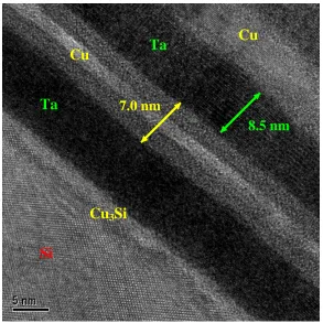
3.3 Transmission Electron Microscopy
A nanolaminate sample from Trial 2 was analyzed using transmission electron
microscopy to determine if a nanolayer structure was formed, the thickness of the layers,
composition of the layers, and microstructures present (crystalline / amorphous).
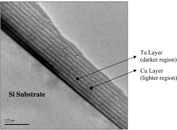
Figure 3.2 clearly shows that a ‘layered’ structure was achieved through the
magnetron sputtering process. The Si substrate and the nanolayered structure are visible in
Figure 3.2. Approximate 18 layers composed of alternating materials can be seen in this
ion-milled sample due to contrast changes. Contrast in this instance is defined in terms of the
difference in intensity between two adjacent areas27. Mass-thickness contrast allows
qualitative determination of the elements in the image due to Rutherford scattering.
Rutherford scattering is a function of atomic number and thickness of the specimen. The
mechanism of mass-thickness contrast is due to higher-Z areas scattering more electrons off
axis, therefore fewer electrons hit the image plane making it appear darker than lower-Z
areas in bright field images27.
In the following images, the change in thickness is negligible, so the contrast should
be due to the change in atomic number. Therefore, for bright field (BF) images, such as
Figure 3.2, the higher atomic number material, in this case Ta (Z=73), will appear darker