Compact SMART CARD
Interface IC
The NCN8025 / NCN8025A is a compact and cost−effective single
smart card interface IC. It is dedicated for 1.8 V / 3.0 V / 5.0 V smart
card reader/writer applications. The card V
CCsupply is provided by a
built−in very low drop out and low noise LDO.
The device is fully compatible with the ISO 7816−3, EMV 4.2,
UICC and related standards including NDS and other STB standards
(Nagravision, Irdeto...). It satisfies the requirements specifying
conditional access into Set−Top−Boxes (STB) or Conditional Access
Modules (CAM and CAS).
This smart card interface IC is available in a QFN−24 package
(NCN8025A) providing all of the industry−standard features usually
required for STB smart card interface. It is also offered in a very
compact package profile, QFN−16 (NCN8025), satisfying the
requirements of cost−efficiency and space−saving requested by CAM
and SIM applications.
For details regarding device implementation refer to application
note AND8003/D, available upon request (please contact your local
ON Semiconductor sales office or representative).
Features
•
Single IC Card Interface
•
Fully Compatible with ISO 7816−3, EMV4.2, UICC and Related
Standards Including NDS and Other STB Standards (Nagravision,
Irdeto...)
•
3 Bidirectional Buffered I/O Level Shifters (C4, C7 and C8)
(QFN−24) − 1 Bidirectional I/O Level Shifter for the QFN−16
compact version
•
1.8 V, 3.0 V or 5.0 V
$
5 % Regulated Card Power Supply
Generation such as ICC
v
70 mA
•
Regulator Power Supply: V
DDP= 2.7 V to 5.5 V (@ 1.8 V),
3.0 V to 5.5 V (@ 3.0 V) & 4.85 V to 5.5 V (@ 5.0 V)
•
Independent Power Supply range on Controller
Interface such as V
DD= 2.7 V to 5.5 V
•
Handles Class A, B and C Smart Cards
•
Short Circuit Protection on all Card Pins
•
Support up to 27 MHz input Clock with Internal
Division Ratio 1/1, 1/2, 1/4 and 1/8 through CLKDIV1
and CLKDIV2
•
ESD Protection on Card Pins up to +8 kV (Human
Body Model)
•
Activation / Deactivation Sequences (ISO7816
Sequencer)
•
Fault Protection Mechanisms Enabling Automatic
Device Deactivation in Case of Overload, Overheating,
Card Take−off or Power Supply Drop−out (OCP, OTP,
UVP)
•
Interrupt Signal INT for Card Presence and Faults
•
External Under−Voltage Lockout Threshold
Adjustment on VDD (PORADJ Pin) (Except QFN−16)
•
Available in 2 Package Formats: QFN−24
(NCN8025A) and QFN−16 (NCN8025)
•
These are Pb−Free Devices
Typical Application
•
Pay TV, Set Top Box Decoder with Conditional Access
and Pay−per−View
•
Conditional Access Module (CAM / CAS)
•
SIM card interface applications (UICC / USIM)
•
Point Of Sales and Transaction Terminals
•
Electronic Payment and Identification
See detailed ordering and shipping information in the package dimensions section on page 13 of this data sheet.
ORDERING INFORMATION MARKING DIAGRAMS
A = Assembly Location L = Wafer Lot Y = Year W = Work Week G = Pb−Free Package
http://onsemi.com
NCN 8025A ALYWG
G
QFN24 MN SUFFIX CASE 485L
1
QFN16 MT SUFFIX CASE 488AK
NCN 8025 ALYWG
G
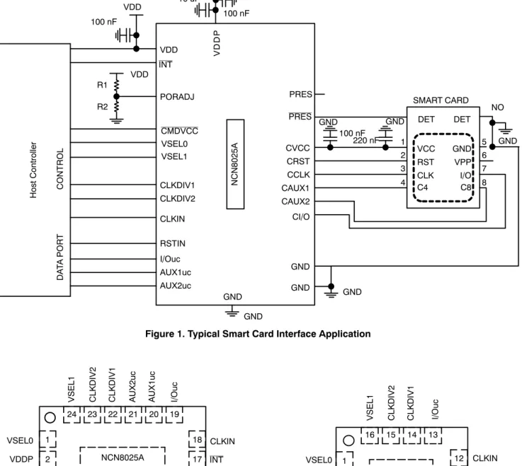
CVCC CAUX1 CCLK I/Ouc CRST PRES VCC RST CLK C4 GND VPP I/O C8 DET DET GND GND 220 nF 1
2 3 4 5 6 7 8 SMART CARD VDD VDD
P VDD VDDP 100 nF CLKDIV2 CLKDIV1 VSEL0 Host Controller DA TA POR T GND NCN8025A GND CAUX2 GND GND CI/O 10 uF AUX1uc AUX2uc PORADJ RSTIN CONTROL 100 nF VDD R1 R2 CLKIN GND VSEL1 GND 100 nF NO
Figure 1. Typical Smart Card Interface Application INT CMDVCC PRES 1 2 3 4 5 6
7 8 9 10 11 12
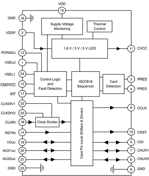
17 16 15 14 13 24 23 22 21 20
18 NCN8025A 25 Exposed Pad GND CAUX2 CI/O PRES VDDP GND VDD RSTIN CLKIN CAUX1 VSEL0 1 2 3 4
16 15 14 13
Exposed Pad VDDP 12 11 10 9
5 6 7 8
CLKIN VDD RSTIN CI/O NCN8025 17 GND VSEL0
Figure 2. NCN8025A − QFN−24 Pinout
(Top View)
Figure 3. NCN8025 − QFN−16 Pinout
(Top View) 19
GND CCLK CRST CVCC
PORADJ
VSEL1 CLKDIV2 CLKDIV1 AUX2uc AUX1uc I/Ouc
INT
CMDVCC
PRES
PRES
INT
VSEL1 CLKDIV2 CLKDIV1 I/Ouc
CCLK CRST CVCC
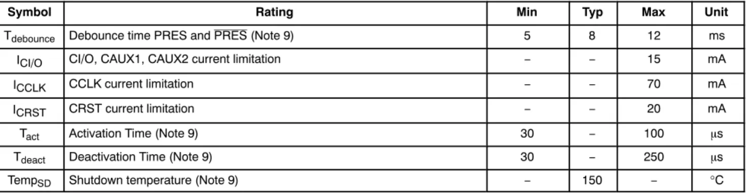
VSEL1 VDDP
17
11 CVCC
24 12
1.8 V / 3 V / 5 V LDO
Card Pin Level Shifters & Drivers
VDD
18 CLKIN
19
25 GND
14 RSTIN
5 CIO
8 GND 10 CRST
9 CCLK 16
GND
4 PRES 3
Supply Voltage Monitoring
Thermal Control
Card Detection Control Logic
and Fault Detection
ISO7816 Sequencer 15
2
20
AUX1uc 7 CAUX1
21 6
AUX2uc CAUX2
1 VSEL0
Clock Divider 23
22 CLKDIV1 CLKDIV2
13 PORADJ
Figure 4. NCN8025A Block Diagram (QFN−24 Pin Numbering)
INT CMDVCC
PRES
I/Ouc
PIN FUNCTION AND DESCRIPTION
Pin (QFN24)
Pin
(QFN16) Name Type Description
1 1 VSEL0 Input Allows selecting card VCC power supply voltage mode (5V/3V or 1.8V/3V)
VSEL0 = Low; CVCC = 5 V when VSEL1 = High or 3 V when VSEL1 = Low VSEL0 = High; CVCC = 1.8 V when VSEL1 = High or 3 V when VSEL1 = Low 2 2 VDDP Power Regulator power supply.
3 3 PRES Input Card presence pin active (card present) when PRES = Low. A built−in debounce timer of about 8 ms is activated when a card is inserted. Convenient for Normally Open (NO) Smart card connector.
4 − PRES Input Card presence pin active (card present) when PRES = High. A built−in debounce timer of about 8 ms is activated when a card is inserted. Convenient for Normally Closed (NC) smart card connector.
5 4 CI/O Input/
Output This pin handles the connection to the serial I/O (C7) of the card connector. Abi−directional level translator adapts the serial I/O signal between the card and the micro controller. A 11 kW (typical) pull up resistor to CVCC provides a High impedance state for the smart card I/O link.
PIN FUNCTION AND DESCRIPTION
Pin
(QFN24) Name Type Description
Pin (QFN16)
6 − CAUX2 Input/
Output This pin handles the connection to the chip card’s serial auxiliary AUX2 I/O pin (C8). Abi−directional level translator adapts the serial I/O signal between the card and the micro controller. A 11 kW (typical) pull up resistor to CVCC provides a High impedance state for the smart card C8 pin.
7 − CAUX1 Input/
Output This pin handles the connection to the chip card’s serial auxiliary AUX1 I/O pin (C4). Abi−directional level translator adapts the serial I/O signal between the card and the micro controller. A 11 kW (typical) pull up resistor to CVCC provides a High impedance state for the smart card C4 pin.
8 − GND Ground Card Ground
9 5 CCLK Output This pin is connected to the CLOCK card connector’s pin (Chip card’s pin C3). The Clock signal comes from the CLKIN input through clock dividers and level shifter.
10 6 CRST Output This pin is connected to the chip card’s RESET pin (C2) through the card connector. A level translator adapts the external Reset (RSTIN) signal to the smart card.
11 7 CVCC Power
Output This pin is connected to the smart card power supply pin (C1). An internal low dropoutregulator is programmable using the pins VSEL0 and VSEL1 to supply either 5 V or 3 V or 1.8 V output voltage. An external distributed ceramic capacitor ranging from 80 nF to 1.2 mF recommended must be connected across CVCC and CGND. This set of capacitor (if distributed) must be low ESR (< 100 mW).
12 8 CMDVCC Input Command VCC pin. Activation sequence Enable/Disable pin (active Low). The activation
sequence is enabled by toggling CMDVCC High to Low and when a card is present. 13 − PORADJ Input Power−on reset threshold adjustment input pin for changing the reset threshold (VDD
UVLO threshold) thanks to an external resistor power divider. Needs to be connected to ground when unused.
14 9 RSTIN Input This Reset input connected to the host and referred to VDD (microcontroller side), is connected to the smart card Reset pin through the internal level shifter which translates the level according to the CVCC programmed value.
15 10 VDD Power
input This pin is connected to the system controller power supply. It configures the level shifterinput stage to accept the signals coming from the controller. A 0.1 mF decoupling capacitor shall be used. When VDD is below 2.30 V typical the card pins are disabled.
16 − GND Ground Ground
17 11 INT Output The interrupt request is activated LOW on this pin. This is enabled when a card is present and the card presence is detected by PRES or PRES pins. Similarly an interrupt is generated when CVCC is overloaded. Inverter output (An open−drain output configuration with 50 kW pull−up resistor is available under request (metal change)).
18 12 CLKIN Input Clock Input for External Clock
19 13 I/Ouc Input /
Output This pin is connected to an external microadapts the serial I/O signal between the smart card and the external controller. A built−controller. A bi−directional level translator−in constant 11 kW (typical) resistor provides a high impedance state.
20 − AUX1uc Input /
Output This pin is connected to an external microadapts the serial C4 signal between the smart card and the external controller. A built−controller. A bi−directional level translator−in constant 11 kW (typical) resistor provides a high impedance state.
21 − AUX2uc Input /
Output This pin is connected to an external microadapts the serial C8 signal between the smart card and the external controller. A built−controller. A bi−directional level translator−in constant 11 kW (typical) resistor provides a high impedance state.
22 14 CLKDIV1 Input This pin coupled with CLKDIV2 is used to program the clock frequency division ratio (Table 2).
23 15 CLKDIV2 Input This pin coupled with CLKDIV1 is used to program the clock frequency division ratio (Table 2).
24 16 VSEL1 Input Allows selecting card VCC power supply voltage.
VSEL0 = Low: CVCC = 5 V when VSEL1 = High or 3 V when VSEL1 = Low. VSEL0 = High: CVCC = 1.8 V when VSEL1 = High or 3 V when VSEL1 = Low. 25 17 GND Ground Regulator Power Supply Ground
NOTE: All information below refers to QFN−24 pin numbering unless otherwise noted. This information can be transposed to the QFN−16 package according to the above “PIN FUNCTION AND DESCRIPTION” Table.
ATTRIBUTES
Characteristics Values
ESD protection
Human Body Model (HBM) (Note 1)
Card Pins (card interface pins 3−11) All Other Pins
Machine Model (MM)
Card Pins (card interface pins 3−11) All Other Pins
8 kV 2 kV 400 V 150 V Moisture sensitivity (Note 2) QFN−24 and QFN−16 Level 1 Flammability Rating Oxygen Index: 28 to 34 UL 94 V−0 @ 0.125 in Meets or exceeds JEDEC Spec EIA/JESD78 IC Latch−up Test
1. Human Body Model (HBM), R = 1500 W, C = 100 pF. 2. For additional information, see Application Note AND8003/D.
MAXIMUM RATINGS (Note 3)
Rating Symbol Value Unit
Regulator Power Supply Voltage VDDP −0.3 ≤ VDDP ≤ 5.5 V
Power Supply from Microcontroller Side VDD −0.3 ≤ VDD ≤ 5.5 V
External Card Power Supply CVCC −0.3 ≤ CVCC ≤ 5.5 V
Digital Input Pins Vin −0.3 ≤ Vin ≤ VDD V
Digital Output Pins (I/Ouc, AUX1uc, AUX2uc, INT) Vout −0.3 ≤ Vout ≤ VDD V
Smart card Output Pins Vout −0.3 ≤ Vout ≤ CVCC V
Thermal Resistance Junction−to−Air (Note 4) QFN−24
QFN−16 RqJA 3748 °C/W
Operating Ambient Temperature Range TA −40 to +85 °C
Operating Junction Temperature Range TJ −40 to +125 °C
Maximum Junction Temperature TJmax +125 °C
Storage Temperature Range Tstg −65 to + 150 °C
Stresses exceeding Maximum Ratings may damage the device. Maximum Ratings are stress ratings only. Functional operation above the Recommended Operating Conditions is not implied. Extended exposure to stresses above the Recommended Operating Conditions may affect device reliability.
3. Maximum electrical ratings are defined as those values beyond which damage to the device may occur at TA = +25°C.
POWER SUPPLY SECTION (VDD = 3.3 V; VDDP = 5 V; Tamb = 25°C; FCLKIN = 10 MHz)
Symbol Rating Min Typ Max Unit
VDDP Regulator Power Supply,
CVCC = 5.0 V, |ICC| ≤ 70 mA (EMV Conditions) |ICC| ≤ 70 mA (NDS Conditions) CVCC = 3.0 V, |ICC| ≤ 70 mA
CVCC = 1.8 V, |ICC| ≤ 70 mA
4.75 4.85 3.0 2.7
5.0 5.0 5.55.5
5.5 5.5
V
IDDP Inactive mode (CMDVCC = High) − − 1 mA
IDDP DC Operating supply current, FCLKIN = 10 MHz, CoutCCLK = 33 pF, |ICVCC| = 0
(CMDVCC = Low) − − 3.0 mA
IDDP DC Operating supply current,
CVCC = 5 V, ICVCC = 70 mA
CVCC= 3 V, ICVCC = 70 mA
CVCC= 1.8 V, ICVCC = 70 mA
− − −
− − −
150 150 150
mA
VDD Operating Voltage 2.7 − 5.5 V
IVDD Inactive mode − standby current (CMDVCC = High) − − 60 mA
IVDD Operating Current − FCLK_IN = 10 MHz , CoutCCLK = 33 pF |ICVCC| = 0 (CMDVCC =
Low) − − 1 mA
UVLOVDD Under Voltage Lock−Out (UVLO), no external resistor at pin PORADJ
(connected to GND), falling VDD level 2.20 2.30 2.40
V UVLOHys UVLO Hysteresis, no external resistor at pin PORADJ (Connected to GND) 50 100 180 mV
PORADJ pin
VPORth+ External Rising threshold voltage on VDD for Power On Reset − pin PORADJ 1.20 1.27 1.34 V
VPORth− External Falling threshold voltage on VDD for Power On Reset − pin PORADJ 1.15 1.20 1.28 V
VPORHys Hysteresis on VPORth (pin PORADJ) 30 80 100 mV
tPOR Width of Power−On Reset pulse (Note 5)
No external resistor on PORADJ
External resistor on PORADJ 44 88 1212 msms
IIL Low level input leakage current, VIL < 0.5 V (Pull−down source current) 5 mA
Low Dropout Regulator
CCVCC Output Capacitance on card power supply CVCC (Note 6) 0.08 0.32 1.2 mF
CVCC Output Card Supply Voltage (including ripple) 1.8 V CVCC mode @ ICC ≤ 70 mA 3.0 V CVCC mode @ ICC ≤ 70 mA
5.0 V CVCC mode @ ICC ≤ 70 mA with 4.85 V ≤ VDDP ≤ 5.5 V (NDS) 5.0 V CVCC mode @ ICC ≤ 70 mA with 4.75 V ≤ VDDP ≤ 5.5 V (EMV)
1.70 2.85 4.75 4.60
1.80 3.00 5.00 5.00
1.90 3.15 5.25 5.25
V V V CVCC Current pulses 15 nAs (t < 400 ns & |ICC| < 100 mA peak) (Note 5)
1.8 V mode / Ripple v 250 mV (2.7 V v VDDP v 5.5 V)
Current pulses 40 nAs (t < 400 ns & |ICC| < 200 mA peak)
3.0 V mode / Ripple v 250 mV (2.9 V v VDDP v 5.5 V)
Current pulses 40 nAs (t < 400 ns & |ICC| < 200 mA peak)
5.0 V mode / Ripple v 250 mV (4.85 V v VDDP v 5.5 V)
1.66 2.70 4.60
1.80 3.00 5.00
1.90 3.30 5.30
V V V ICVCC Card Supply Current
@ CVCC = 1.8 V @ CVCC = 3.0 V @ CVCC = 5.0 V
70 70 70
mA
ICVCC_SC Short −Circuit Current − CVCC shorted to ground 120 150 mA
DVCVCC Output Card Supply Voltage Ripple peak−to−peak − fripple = 100 Hz to 200 MHz (load
transient frequency with 65 mA peak current and 50% Duty Cycle) (Note 5) 300 mV CVCCSR Slew Rate on CVCC turn−on / turn−off (Note 5) 0.22 V/ms
5. Guaranteed by design and characterization.
HOST INTERFACE SECTION CLKIN, RSTIN, I/Ouc, AUX1uc, AUX2uc, CLKDIV1, CLKDIV2, CMDVCC, VSEL0, VSEL1 (VDD =
3.3 V; VDDP = 5 V; Tamb = 25°C; FCLKIN = 10 MHz)
Symbol Rating Min Typ Max Unit
FCLKIN Clock frequency on pin CLKIN (Note 7) − − 27 MHz
VIL Input Voltage level Low: CLKIN, RSTIN, CLKDIV1, CLKDIV2, CMDVCC, VSEL0,
VSEL1 −0.3 − 0.3 x VDD V
VIH Input Voltage level High: CLKIN, RSTIN, CLKDIV1, CLKDIV2, CMDVCC, VSEL0,
VSEL1 0.7 x VDD − VDD + 0.3 V
|IIL| CLKDIV1, CLKDIV2, CMDVCC, RSTIN, CLKIN, VSEL0, VSEL1 Low Level Input
Leakage Current, VIL = 0 V
− − 1 mA
|IIH| CLKDIV1, CLKDIV2, CMDVCC, RSTIN, CLKIN, VSEL0, VSEL1 Low Level Input
Leakage Current, VIH = VDD
− − 1 mA
VIL Input Voltage level Low: I/Ouc, AUX1uc, AUX2uc −0.3 0.5 V
VIH Input Voltage level High: I/Ouc, AUX1uc, AUX2uc 0.7 x VDD VDD + 0.3 V
|IIL | I/Ouc, AUX1uc, AUX2uc Low level input leakage current, VIL = 0 V − − 600 mA
|IIH| I/Ouc, AUX1uc, AUX2uc High level input leakage current, VIH = VDD − − 10 mA
VOH
VOL
tRi/Fi
tRo/Fo
I/Ouc, AUX1uc, AUX2uc data channels, @ Cs v 30 pF
High Level Output Voltage (CRD_I/O = CAUX1 = CAUX2 = CVCC) IOH = −40 mA for VDD > 2 V (IOH = −20 mA for VDDv 2 V)
Low Level Output Voltage (CRD_I/O = CAUX1 = CAUX2 = 0 V) IOL= + 1 mA
Input Rising/Falling times (Note 7) Output Rising/Falling times (Note 7)
0.75 x VDD
0
− −
− − − −
VDD + 0.1
0.3 1.2 0.1
V V
ms
ms
Rpu I/0uc, AUX1uc, AUX2uc Pull Up Resistor 8 11 16 kW
VOH Output High Voltage
INT @ IOH = −15 mA (source) 0.75 x VDD − −
V VOL Output Low Voltage
INT @ IOL = 2 mA (sink) 0 − 0.30
V
RINT INT Pull Up Resistor (open−drain output configuration option) (Note 8) 40 50 60 kW
7. Guaranteed by design and characterization.
SMART CARD INTERFACE SECTION CI/O, CAUX1, CAUX2, CCLK, CRST, PRES, PRES (VDD = 3.3 V; VDDP = 5 V; Tamb = 25°C;
FCLKIN = 10 MHz)
Symbol Rating Min Typ Max Unit
VOH VOL tR tF tR/F td
CRST @ CVCC = 1.8 V, 3.0 V, 5.0 V
Output RESET VOH @ Irst = −200 mA
Output RESET VOL @ Irst = 200 mA
Output RESET Rise time @ Cout = 100 pF (Note 9)
Output RESET Fall time @ Cout = 100 pF (Note 9)
Output Rise/Fall times @ CVCC = 1.8 V & Cout = 100 pF (Note 9)
RSTIN to CRST delay − Reset enabled (Note 9)
0.9 x CVCC 0 − − − − − − − − − − CVCC 0.20 100 100 200 2 V V ns ns ns ms FCRDCLK VOH VOL FDC trills tulsa SR
CCLK @ CVCC = 1.8 V, 3.0 V or 5.0 V Output Frequency (Note 9)
Output CCLK VOH @ Iclk = −200 mA
Output CCLK VOL @ Iclk = 200 mA
Output Duty Cycle (Note 9) Rise & Fall time
Output CCLK Rise time @ Cout = 33 pF (Note 9)
Output CCLK Fall time @ Cout = 33 pF (Note 9)
Slew Rate @ Cout = 33 pF (CVCC = 3.0 V or 5.0 V) (Note 9)
−
0.9 x CVCC 0 45 − − 0.2 − − − − − − − 27 CVCC +0.2 55 16 16 − MHz V V % ns ns V/ns VIH VIL
|IIL|
|IIH|
VOH
VOL
tRi / Fi
tRo / Fo
CAUX1, CAUX2, CI/O @ CVCC = 1.8 V, 3.0 V, 5.0 V Input Voltage High Level
1.8 V Mode 3.0 V Mode 5.0 V Mode Input Voltage Low Level
1.8 V mode
3.0 V and 5.0 V modes Low Level Input current VIL = 0 V
High Level Input current VIH = CVCC
Output VOH
@ IOH = −40 mA for CVCC = 3.0 V and 5.0 V
@ IOH = −20 mA for CVCC = 1.8 V
Output VOL
@ IOL = 1 mA, VIL = 0 V
Input Rising/Falling times (Note 9)
Output Rising/Falling times / Cout = 80 pF (Note 9)
1.2 1.6 2.3 −0.30 −0.30 − −
0.75 x CVCC 0.75 x CVCC
0 − − − − − − − − − − − −
CVCC + 0.3 CVCC + 0.3 CVCC + 0.3
0.50 0.80 600 10 CVCC + 0.1 CVCC + 0.1
0.30 1.2 0.1 V V V V V mA mA V V V ms ms Fbidi Maximum data rate through bidirectional I/O, AUX1 & AUX2 channels (Note 9) − − 1 MHz
RPU CAUX1, CAUX2, CI/O Pull− Up Resistor 8 11 16 kW
tIO Propagation delay IOuc −> CI/O and CI/O −> IOuc (falling edge) (Note 9) − − 200 ns
tpu Active pull−up pulse width buffers I/O, AUX1 and AUX2 (Note 9) − − 200 ns
Cin Input Capacitance on data channels − − 10 pF
VIH
VIL
PRES, PRES
Card Presence Voltage High Level
Card Presence Voltage Low Level 0.7 x V−0.3DD −− V0.3 x VDD + 0.3DD
V
|IIH|
|IIL|
PRES, PRES
High level input leakage current, VIH = VDD
PRES PRES
Low level input leakage current, VIL = 0 V
PRES PRES 5 5 10 1 1 10 mA
SMART CARD INTERFACE SECTION CI/O, CAUX1, CAUX2, CCLK, CRST, PRES, PRES (VDD = 3.3 V; VDDP = 5 V; Tamb = 25°C;
FCLKIN = 10 MHz)
Symbol Rating Min Typ Max Unit
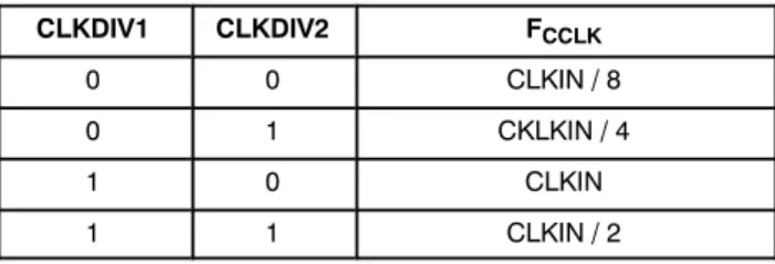
Tdebounce Debounce time PRES and PRES (Note 9) 5 8 12 ms
ICI/O CI/O, CAUX1, CAUX2 current limitation − − 15 mA
ICCLK CCLK current limitation − − 70 mA
ICRST CRST current limitation − − 20 mA
Tact Activation Time (Note 9) 30 − 100 ms
Tdeact Deactivation Time (Note 9) 30 − 250 ms
TempSD Shutdown temperature (Note 9) − 150 − °C
9. Guaranteed by design and characterization. POWER SUPPLY
The NCN8025 / NCN8025A smart card interface has two
power supplies: V
DDand V
DDP.
V
DDis common to the system controller and the interface.
The applied V
DDrange can go from 2.7 V up to 5.5 V. If V
DDgoes below 2.30 V typical (UVLO
VDD) a power−down
sequence is automatically performed. In that case the
interrupt (INT) pin is set Low.
A Low Drop−Out (LDO) and low noise regulator is used
to provide the 1.8 V, 3 V or 5 V power supply voltage
(CVCC) to the card. V
DDPis the LDO’s input voltage.
CVCC is the LDO output. The typical distributed reservoir
output capacitor connected to CVCC is 100 nF + 220 nF. The
capacitor of 100 nF is connected as close as possible to the
CVCC’s pin and the 220 nF one as close as possible to the
card connector C1 pin. Both feature very low ESR values
(lower than 50 m
W
). The decoupling capacitors on V
DDand
V
DDPrespectively 100 nF and 10
m
F + 100 nF have also to
be connected close to the respective IC pins.
The CVCC pin can source up to 70 mA at 1.8 V, 3 V and
5 V continuously over the V
DDPrange (see corresponding
specification table), the absolute maximum current being
internally limited below 150 mA (Typical at 120 mA).
The card V
CCvoltage (CVCC) can be programmed with
the pins VSEL0 and VSEL1 and according to the below table:
Table 1. CVCC PROGRAMMING
VSEL0 VSEL1 CVCC
0 0 3.0 V
0 1 5.0 V
1 0 3.0 V
1 1 1.8 V
VSEL0 can be used to select the CVCC programming
mode which can be 5V/3V (VSEL0 connected to Ground)
or 1.8V/3V (VSEL0 connected to V
DD). VSEL0 and
VSEL1 are usually programmed before activating the smart
card interface that is when /CMDVCC is High.
There’s no specific sequence for applying V
DDor V
DDP.
They can be applied to the interface in any sequence. After
SUPPLY VOLTAGE MONITORING
The supply voltage monitoring block includes the
Power−On Reset (POR) circuitry and the under−voltage
lockout (UVLO) detection (V
DDvoltage dropout
detection). PORADJ pin allows the user, according to the
considered application, to adjust the V
DDUVLO threshold.
If not used PORADJ pin is connected to Ground
(recommended even if it may be left unconnected).
The input supply voltage is continuously monitored to
prevent under voltage operation. At power up, the system
initializes the internal logic during POR timing and no further
signal can be provided or supported during this period.
The system is ready to operate when the input voltage has
reached the minimum V
DD. Considering this, the NCN8025
/ NCN8025A will detect an Under−Voltage situation when
the input supply voltage will drop below 2.30 V typical.
When V
DDgoes down below the UVLO falling threshold a
deactivation sequence is performed.
The device is inactive during power−on and power−off of
the V
DDsupply (8 ms reset pulse).
PORADJ pin is used to modify the UVLO threshold
according to the below relationship considering an external
resistor divider R1 / R2 (see block diagram Figure 1):
UVLO+R1)R2
R2 VPOR (eq. 1)
If PORADJ is connected to Ground the V
DDUVLO
threshold (V
DDfalling) is typically 2.30 V. In some cases it
can be interesting to adjust this threshold at a higher value
and by the way increase the V
DDsupply dropout detection
level which enables a deactivation sequence if the V
DDvoltage is too low.
For example, there are microcontrollers for which the
minimum supply voltage insuring a correct operating is
higher than 2.6 V; increasing UVLO
VDD(V
DDfalling) is
consequently necessary. Considering for instance a resistor
bridge with R1 = 56 k
W
, R2 = 42 k
W
and V
POR−= 1.27 V
typical the V
DDdropout detection level can be increased up
to:
CLOCK DIVIDER:
The input clock can be divided by 1/1, 1/2, 1/4, or 1/8,
depending upon the specific application, prior to be applied
to the smart card driver. These division ratios are
programmed using pins CLKDIV1 and CLKDIV2 (see
Table 2). The input clock is provided externally to pin
CLKIN.
Table 2. CLOCK FREQUENCY PROGRAMMING
CLKDIV1 CLKDIV2 FCCLK
0 0 CLKIN / 8
0 1 CKLKIN / 4
1 0 CLKIN
1 1 CLKIN / 2
The clock input stage (CLKIN) can handle a 27 MHz
maximum frequency signal. Of course, the ratio must be
defined by the user to cope with Smart Card considered in
a given application
In order to avoid any duty cycle out of the 45% / 55%
range specification, the divider is synchronized by the last
flip flop, thus yielding a constant 50% duty cycle, whatever
be the divider ratio 1/2, 1/4 or 1/8. On the other hand, the
output signal Duty Cycle cannot be guaranteed 50% if the
division ratio is 1 and if the input Duty Cycle signal is not
within the 46% − 56% range at the CLKIN input.
When the signal applied to CLKIN is coming from the
external controller, the clock will be applied to the card
under the control of the microcontroller or similar device
after the activation sequence has been completed.
DATA I/O, AUX1 and AUX2 LEVEL SHIFTERS
The three bidirectional level shifters I/O, AUX1 and
AUX2 adapt the voltage difference that might exist between
the micro−controller and the smart card. These three
channels are identical. The first side of the bidirectional
level shifter dropping Low (falling edge) becomes the driver
side until the level shifter enters again in the idle state pulling
High CI/O and I/Ouc.
Passive 11 k
W
pull−up resistors have been internally
integrated on each terminal of the bidirectional channel. In
addition with these pull−up resistors, an active pull−up
circuit provides a fast charge of the stray capacitance.
The current to and from the card I/O lines is limited
internally to 15 mA and the maximum guaranteed frequency
on these lines is 1 MHz.
STANDBY MODE
After a Power−on reset, the circuit enters the standby mode.
A minimum number of circuits are active while waiting for
the microcontroller to start a session:
−
All card contacts are inactive
−
Pins I/Ouc, AUX1uc and AUX2uc are in the
high−impedance state (11 k
W
pull−up resistor to V
DD)
−
Card pins are inactive and pulled Low
−
Supply Voltage monitoring is active
POWER−UP
In the standby mode the microcontroller can check the
presence of a card using the signals INT and CMDVCC as
shown in Table 3:
Table 3. CARD PRESENCE STATE
INT CMDVCC State
HIGH HIGH Card present
LOW HIGH Card not present
If a card is detected present (PRES or PRES active) the
controller can start a card session by pulling CMDVCC
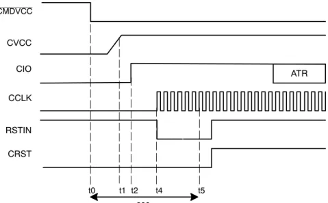
Low. Card activation is run (t0, Figure 6). This Power−Up
Sequence makes sure all the card related signals are LOW
during the CVCC positive going slope. These lines are
validated when CVCC is stable and above the minimum
voltage specified. When the CVCC voltage reaches the
programmed value (1.8 V, 3.0 V or 5.0 V), the circuit
activates the card signals according to the following
sequence (Figure 6):
−
CVCC is powered−up at its nominal value (t1)
−
I/O, AUX1 and AUX2 lines are activated (t2)
−
Then Clock is activated and the clock signal is applied
to the card (typically 500 ns after I/Os lines) (t3)
−
Finally the Reset level shifter is enabled (typically
500 ns after clock channel) (t4)
The clock can also be applied to the card using a
RSTIN
mode
allowing controlling the clock starting by setting
RSTIN Low (Figure 5). Before running the activation
sequence, that is before setting Low CMDVCC RSTIN is set
High. The following sequence is applied:
−
The Smart Card Interface is enable by setting
CMDVCC LOW (RSTIN is High).
−
Between t2 (Figure 5) and t5 = 200
m
s, RSTIN is reset
to LOW and CCLK will start precisely at this moment
allowing a precise count of clock cycles before toggling
CRST Low to High for ATR (Answer To Reset)
request.
−
CRST remains LOW until 200
m
s; after t5 = 200
m
s
CRST is enabled and is the copy of RSTIN which has
no more control on the clock.
If controlling the clock with RSTIN is not necessary
(
Normal Mode
), then CMDVCC can be set LOW with
RSTIN LOW. In that case, CLK will start minimum 500 ns
after the transition on I/O (Figure 6), and to obtain an ATR,
CRST can be set High by RSTIN also about 500 ns after the
clock channel activation (T
act).
The internal activation sequence activates the different
channels according to a specific hardware built−in
sequencing internally defined but at the end the actual
activation sequencing is the responsibility of the application
software and can be redefined by the micro−controller to
comply with the different standards and the different ways
the standards manage this activation (for example light
differences exist between the EMV and the ISO7816
standards).
CRST CVCC CIO
CCLK
ATR
RSTIN
Figure 5. Activation Sequence − RSTIN Mode (RSTIN Starting High)
CMDVCC
t0 t1 t2 t4 t5
~200 ms
CRST CVCC CIO CCLK
ATR
RSTIN
Figure 6. Activation Sequence − Normal Mode
CMDVCC
t0 t1 t2t3 t4 Tact
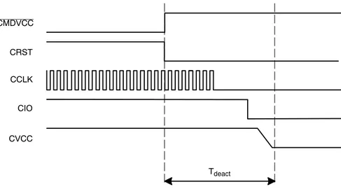
POWER−DOWN
When the communication session is completed the
NCN8025 / NCN8025A runs a deactivation sequence by
setting High CMDVCC. The below power down sequence
is executed:
−
CRST is forced to Low
−
CCLK is set Low 12
m
s after CRST.
−
CI/O, CAUX1 and CAUX2 are pulled Low
−
Finally CVCC supply can be shut−off.
CRST
CVCC CIO CCLK
Figure 7. Deactivation Sequence CMDVCC
Tdeact
FAULT DETECTION
In order to protect both the interface and the external smart
card, the NCN8025 / NCN8025A provides security features
to prevent failures or damages as depicted here after.
−
Card extraction detection
−
V
DDunder voltage detection
−
Short−circuit or overload on CVCC
−
DC/DC operation: the internal circuit continuously
senses the CVCC voltage (in the case of either over or
under voltage situation).
−
DC/DC operation: under−voltage detection on V
DDP−
Overheating
−
Card pin current limitation: in the case of a short circuit
to ground. No feedback is provided to the external
MPU.
PRES
CVCC /INT
debounce debounce
Powerdown resulting
of card extraction Powerdown causedby short−circuit Figure 8. Fault Detection and Interrupt Management
CMDVCC
Interrupt Pin Management:
A card session is opened by toggling CMDVCC High to
Low.
Before a card session, CMDVCC is supposed to be in a
High position. INT is Low if no card is present in the card
connector (Normally open or normally closed type). INT is
High if a card is present. If a card is inserted (INT = High)
and if V
DDdrops below the UVLO threshold then INT pin
drops Low immediately. It switches High when V
DDincreases again over the UVLO limit (including hysteresis),
a card being still present.
During a card session, CMDVCC is Low and INT pin
goes Low when a fault is detected. In that case a deactivation
is immediately and automatically performed (see Figure 7).
When the microcontroller resets CMDVCC to High it can
sense the INT level again after having got completed the
deactivation.
As illustrated by Figure 8 the device has a debounce timer
of 8 ms typical duration. When a card is inserted, output INT
goes High only at the end of the debounce time. When the
card is removed a deactivation sequence is automatically
and immediately performed and INT goes Low.
ESD PROTECTION
The NCN8025 / NCN8025A includes devices to protect
the pins against the ESD spike voltages. To cope with the
different ESD voltages developed across these pins, the built
in structures have been designed to handle either 2 kV, when
related to the micro controller side, or 8 kV when connected
with the external contacts (HBM model). Practically, the
CRST, CCLK, CI/O, CAUX1, CAUX2, PRES and PRES
pins can sustain 8 kV. The CVCC pin has the same ESD
protection and can source up to 70 mA continuously, the
absolute maximum current being internally limited with a
max at 150 mA. The CVCC current limit depends on V
DDPand CVCC.
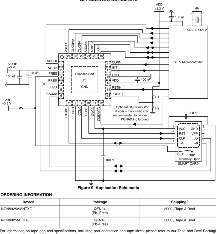
APPLICATION SCHEMATIC
3.3 V Microcontroller
VCC RST CLK C4
GND VPP I/O C8 1
2 3 4
5 6 7 8
SMART CARD R1
R2 VDD +3.3 V
DET
Normally Open VDD
+3.3 V VDDP +5 V
+ 100 nF
XTAL1 XTAL2
100 nF CAUX2
CI/O PRES VDDP
VDD RSTIN CLKIN VSEL0
1 2 3 4 5 6
7 8 9 10 11 12 17 16 15 14 13 24 23 22 21 20 19
18 Exposed Pad
25 GND
220 nF 100 nF
GND
100 nF
Figure 9. Application Schematic
VSEL1 CLKDIV2 CLKDIV1 AUX2uc AUX1uc I/Ouc
CAUX1 GND CCLK CRST CVCC
PORADJ
Optional R1/R2 resistor divider − if not used it is recommended to connect PORADJ to Ground 10 mF
INT PRES
CMDVCC
ORDERING INFORMATION
Device Package Shipping†
NCN8025AMNTXG QFN24
(Pb−Free) 3000 / Tape & Reel
NCN8025MTTBG QFN16
(Pb−Free) 3000 / Tape & Reel
†For information on tape and reel specifications, including part orientation and tape sizes, please refer to our Tape and Reel Packaging Specifications Brochure, BRD8011/D.
PACKAGE DIMENSIONS
QFN24, 4x4, 0.5PCASE 485L−01 ISSUE A
NOTES:
1. DIMENSIONING AND TOLERANCING PER ASME Y14.5M, 1994.
2. CONTROLLING DIMENSION: MILLIMETERS. 3. DIMENSION b APPLIES TO PLATED TERMINAL
AND IS MEASURED BETWEEN 0.25 AND 0.30 MM FROM TERMINAL.
4. COPLANARITY APPLIES TO THE EXPOSED PAD AS WELL AS THE TERMINALS.
SEATING PLANE
D
B
0.15 C
A2 A A3
A
E
PIN 1 IDENTIFICATION
2X 0.15 C
2X
0.08 C 0.10 C
A1 C
DIM MIN MAX MILLIMETERS A 0.80 1.00 A1 0.00 0.05 A2 0.60 0.80 A3 0.20 REF
b 0.20 0.30 D 4.00 BSC D2 2.70 2.90
E 4.00 BSC E2 2.70 2.90
e 0.50 BSC L 0.30 0.50
24X
L
D2
b 1
6 7
18 13
19
e
12
E2 e
24
0.10 B
0.05 A C C
PACKAGE DIMENSIONS
QFN16, 3x3, 0.5 PCASE 488AK ISSUE O
16X
SEATING PLANE
L
D
E
0.15 C
A A1
e D2
E2
b
1 4
5 8
12 9
16 13
NOTES:
1. DIMENSIONING AND TOLERANCING PER ASME Y14.5M, 1994.
2. CONTROLLING DIMENSION: MILLIMETERS. 3. DIMENSION b APPLIES TO PLATED
TERMINAL AND IS MEASURED BETWEEN 0.25 AND 0.30 MM FROM TERMINAL. 4. COPLANARITY APPLIES TO THE EXPOSED
PAD AS WELL AS THE TERMINALS. 5. Lmax CONDITION CAN NOT VIOLATE 0.2 MM
SPACING BETWEEN LEAD TIP AND FLAG.
ÇÇÇ
ÇÇÇ
B A
0.15 C
TOP VIEW
SIDE VIEW
BOTTOM VIEW
PIN 1 LOCATION
0.10 C
0.08 C
(A3)
C
16 X
16X NOTE 5
0.10 C 0.05 C
A B
NOTE 3
K
16X
EXPOSED PAD
DIM MIN MAX MILLIMETERS A 0.70 0.80
A1 0.00 0.05
A3 0.20 REF
b 0.18 0.30
D 3.00 BSC
D2 1.65 1.85
E 3.00 BSC
E2 1.65 1.85
e 0.50 BSC
K 0.20 −−− L 0.30 0.50
ON Semiconductor and are registered trademarks of Semiconductor Components Industries, LLC (SCILLC). SCILLC reserves the right to make changes without further notice to any products herein. SCILLC makes no warranty, representation or guarantee regarding the suitability of its products for any particular purpose, nor does SCILLC assume any liability arising out of the application or use of any product or circuit, and specifically disclaims any and all liability, including without limitation special, consequential or incidental damages. “Typical” parameters which may be provided in SCILLC data sheets and/or specifications can and do vary in different applications and actual performance may vary over time. All operating parameters, including “Typicals” must be validated for each customer application by customer’s technical experts. SCILLC does not convey any license under its patent rights nor the rights of others. SCILLC products are not designed, intended, or authorized for use as components in systems intended for surgical implant into the body, or other applications intended to support or sustain life, or for any other application in which the failure of the SCILLC product could create a situation where personal injury or death may occur. Should Buyer purchase or use SCILLC products for any such unintended or unauthorized application, Buyer shall indemnify and hold SCILLC and its officers, employees, subsidiaries, affiliates, and distributors harmless against all claims, costs, damages, and expenses, and reasonable attorney fees arising out of, directly or indirectly, any claim of personal injury or death associated with such unintended or unauthorized use, even if such claim alleges that SCILLC was negligent regarding the design or manufacture of the part. SCILLC is an Equal Opportunity/Affirmative Action Employer. This literature is subject to all applicable copyright laws and is not for resale in any manner.
PUBLICATION ORDERING INFORMATION
N. American Technical Support: 800−282−9855 Toll Free