:[
[
[
(:
[
I
l
r
IJ
[
[
I'
II
r
I"
('
[
[
[
PRELIMINARY
CIP /2000 COMPUTER
REFERENCE MANUAL
September, 1969
iI1
lJj
iI!
lIJ
[
[
I
I
I
~I
I
II
I
[
[
I
I
I
I
[
[
l
r
r
I~
I
I
1.
2.
3.
4.
5. 6.
TABLE OF CONTENTS
SYSTEM DESIGN FEATURES 1
General Characteristics 2
CIP / 2100 Macro-Programmed Computer 2
SYSTEM ORGANIZATION 3
General Description 3
Registers and File 3
Core Memory
.
6Read Only Storage 6
Command Formats 7
Status and Condition Flags 8
Command Timing 9
MICROCOMMAND REPERTOIRE 11
Literal Commands 11
Operate Commands 14
Execute Command 21
INPUT/OUTPUT 23
General Description 23
Serial Teletype 23
Direct Memory Access 23
Byte I/O Bus
.
25CIP / 2100 Byte I/O Standards 28
OPTIONS 33
OPERATOR CONTROLS 37
Consoles 37
Displays 38
Switches 38
[
I
[
1
I
I'
I
I
I
I
I
I
1
I
I:
I.
I
APPENDIXES
[
A. SYMBOLIC LANGUAGE 41
I
C. B. MICROCOMMANDS ALPHABETIC LIST OF COMMANDS . 43 44I
I
I
I LLUSTRA TIONS
I
l. CIP / 2000 Block Diagram 4I
2. 3. Input/Output Organization Bus Lines . 24 264. Control Console 37
I
I
I
TABLES
I'
I,
l. File Register 0 Flags .62. Register Designators for Operate Commands .8
I
3. Internal Status Bits .84. Byte I/O Control Modes 25
I:
(
II
;f
~
I
·1··· , ,
I
I
I
I
I
I
I
I
1
I
1
,.,
1
I
I
I
[
r
('
I
r
I
[
I
I
I
I', '
I :I'
I
[
I'
1. SYSTEM DESIGN FEATURES
CIP / 2000 is a small byte oriented microprogrammed computer designed for dedicated applications. The functional, mechanical and electrical design of the computer result in a set of functional elements which can be tailored to specific application requirements. The CIP / 2000 is a basic set of hardware which forms the basis for a series of machines.
The design concepts embodied in the CIP /2000 provide a unique combination of features unavailable in other small computer systems. These include:
Microprogramming
The CIP / 2000 incorporates a set of commands that exert powerful micro-control over the machine's data manipulation paths and control. Command sequences which form microprograms are stored in a read only storage. The CIP /2000 can be programmed to emulate instructions of general or special purpose computer or to perform specific applications.
Speed
The machine incorporates a 1.1 microsecond core memory cycle time and a 220 nanosecond command execution time. This speed permits rapid emulation of macro instructions and can be used to minimize interface hardware by applying the speed of the machine to interface functions.
Modularity
The modular electrical and mechanical design results in the flexibility needed to apply the CIP / 2000 to a wide range of applications. The modular design of the core memory read only storage, processor options, and input/output elements permits expansion of the system as required. The compact 8-3/4 inch high enclosure has a number of spare circuit board slots and ample power for system and peripheral interfaces even when the processor is fully expanded.
Low Cost
The CIP / 2000 uses TTL monolithic integrated circuits including a large number of the medium scale integration type for savings in parts and assembly time. The use of a read only storage for control further reduces the number of circuits that might otherwise be required to provide the same functional capability. Packaging and powering of the CIP / 2000 has been designed for small "micro" systems resulting in a savings in system cost.
Software
Programs for the CIP / 2000 include: An assembler written in FORTRAN for use on large-scale computers, utility programs for generating the read only storage maps, and processor and memory diagnostics.
GENERAL CHARACTERISTICS The advanced features and operating characteristics include:
• Memory addressing to 32k • 4096 byte memory modules
• 16,384 bytes of memory in basic 8-3/4 inch high cabinent • 1.1 microsecond memory speed (full cycle)
• 8, 9 or 10 bit memory bytes for efficient character handling; extra bits for memory parity and special application
• direct memory access (DMA) option • 16 general-purpose eight-bit file registers
• up to 1024 words of read only storage in 256 word modules • 220 nanosecond microcommand execution time
• real-time clock (optional) • memory protect (optional)
• power-fail option for automatic shutdown in the event of a power failure, and automatic startup when power returns
• seven I/O transfer modes • 15 basic commands
• three versions of control consoles • TTL integrated circuitry
• operating temperature range O°C to 50°C
• dImensions: 8-3/4 inches high, 19 inches wide, 23 inches deep • power: 115/230 vac, 50-60 cycle
CIP / 2100 MACRO-PROGRAMMED COMPUTER
The CIP / 2100 is a microprogrammed adaptation of the elP / 2000 hardware. The microprogram (firmware) converts the basic CIP / 2000 system into a software programmable macro level general purpose computer. Detailed description of the CIP
f
2100can be found in the CIP / 2100 Reference Manual. The salient characteristics of this machine include:
• variable length instructions
• 16-bit accumulator, extended accumulator, and index register • eight memory referencing address modes
• multiply and divide
• variable 8,16,24, and 32-bit operations
• programmed, buffered concurrent, and DMA input/output transfers • priority interrupt system
• software includes: two pass assembler, and teletype operating system • bootstrap loader in non-volatile read only storage
• up to 64 priority interrupts expandable in groups of 8
4
~
•.It
I
I
I
I
I
I
I
-I.
I
[
[
I:
I
(
I
I
I
I:
r
I
(
2. SYSTEM ORGANIZATION GENERAL DESCRIPTION
The CIP / 2000 is a bus organized machine built around a file of 16 programmable registers and employing microprogrammed control. The basic elements of the machine are shown in the block diagram of Figure l.
The machine executes 15 basic commands with many variations. All commands are 16 bits in length and are one of two formats. CIP / 2000 programs, which are known as microprograms, are placed in a read only storage and thereafter become a part of the machine's hardware. The program can be changed by replacing the printed circuit boards containing the read only storage. The commands read out of the store control all aspects of the operation of the basic machine and are executed in a single machine clock cycle.
The eight-bit arithmetic/logic unit performs all manipulation of data including: addition, logical AND, logical OR, logical exclusive OR, and one bit left and right shifts. The output of this logic network is the A-bus which is the input to the file and other machine registers. All byte data movement is performed over this bus. The output of the file is one of the inputs to the arithmetic/logic unit; the other is the B bus. Inputs to this bus are determined by the command, its options, and the I/O mode. Bus inputs are the true output of the T register, the complement output of the T register, the Input bus and the eight bit literal contained in some commands.
The memory data and address busses communicate between the four memory modules, the processor and the DMA option. Either the processor or the DMA may operate with the memory, with the DMA having top priority.
The registers, file, arithmetic/logic unit and bussing are organized onto two identical "data" printed circuit boards-a four bit slice of the machine on each board. All command decoding, control, clock generation and memory timing are located on a single "control" board. Each 256 words of read only storage requires a single board and the core memory requires a pair of boards.
REGISTERS AND FILE
There are eight registers and 16 file registers. Each of the registers has a specific use in the processor, while the file is used for general storage and flags.
T Register
The eight-bit T register serves as the operand register for most of the operate class commands, and as a buffer register for output and memory operations. The T register is expanded to nine bits when the spare memory bit option is included in the processor. Both the true and complement output of the T register can be gated to the B-bus as an operand. When both the contents of T and its complement are selected as operands, the effective operand is all I-bits; while if neither is selected the operand is all a-bits.
J
~
M Register N Register
(8) (8)
"'"-.... Direct Memory Address Bus
...
Memory
..
..
AccessCore Memory
~ 0-32K Bytes
Memory Data Bus
:
Control 110 Control.... Register
I
Output Bus
+
+
Input Bus T Register
I
(8) File
Registers (16x8)
~
,
I
B Bus
..
I','
I i 'Link ~ Arithmetic/Logic Unit Flags
(1 ) ~ (8)
A Bus
i
i
+
L Register Console Internal (10)
Status
•
~Read-Only Storage
U Register 256-1024 Words
(16) (8)
R Bus
•
R Register (16)
•
Command Qecode
I
and Control
[image:10.612.84.527.60.650.2]i
I
FIGURE 1. CIP/2000 BLOCK DIAGRAM
I
6
I
('
(
I
I
I
I
[
[
l
f
I
I
(
(
I
(
M Register
The eight-bit M register contains the seven high order bits of the processor memory address. This register is gated onto the memory address bus at all times except when a DMA operation is in process.
N Register
The eight-bit N register contains the eight low order bits of the processor memory address. This register is gated onto the memory address bus at all times except when a DMA memory operation is in process.
L Register
The IO-bit L register is the machines' program counter and contains the read only storage address of the next command to be executed, unless altered by a Jump command. The eight low order bits of the L register are a counter which is incremented by one at each clock time when the processor is running unless, there is a command execution delay imposed.
U Register
The eight-bit U register is used to modify the output of the read only storage. For commands with O's in the four high order bits or 1 's in bit 15 and the three low order bits, the contents of the U register is inclusive -ORed with the eight high order bits of the read only storage output as it is gated into the R register. This allows for dynamic modification and changing of operation codes and file register designators.
R Register
The 16-bit register holds the command being executed. Its output is decoded and controls the operation of the processor at each clock time.
LINK Register
The one-bit LINK register holds the adder's high order carry from Add, Subtract, and Compare commands and the shifted off end bit from the Shift command.
I/O Control Register
This three-bit register generates the control signals for the I/O bus by a decoding of the register outputs. It is loaded and cleared by a Control command and therefore the timing of I/O control signals is under command control. There are three output modes and four input modes. The high order bit of the register is the input flag. When this bit is a I-bit the Input bus is substituted for the T register when it is selected and the Input bus is the source of data when executing an external I/O Control command.
File Registers
The file consists of 16 eight-bit operational registers. All commands except the load register (1) specify a file register to be operated on or to provide an operand. All file registers are
functionally identical except for file register 0 which contains eight flags, and cannot be used for general storage. The flags of file register 0 are given in Table 1.
BIT
o
1 2
3
4
5 6 7
TABLE 1. FILE REGISTER 0 FLAGS
FLAG
Overflow Result Condition Negative Result Condition Zero Result Condition Concurrent I/O Request Line I nternal Interrupt
I/O Reply Line
Serial Teletype and/or T 8 External Interrupt Line
CORE MEMORY
The magnetic core memory is organized into two board pluggable modules of 4096 bytes. The memory is addressed at the byte level and each byte contains 8, 9, or 10 bits. The ninth and tenth bits are devoted to the spare memory bit and memory parity bit options. Memory may be expanded up to four modules (16,384 bytes) within the basic 8-3/4 inches cabinet. Addressing to 32,768 bytes permits modular exvansion using an auxiliary cabinet.
The memory is operated in read/write and full/half cycle operations. The full-cycle memory timing is five 220 ns clock cycles
0.1
microseconds); the half-cycle timing in the system is three clock cycles (660 ns). For a read operation, the accessed data is placed in the T register two clock cycles after the start of the memory operation. Full cycle regeneration of the data in the memory does not require the use of the T register and T may be modified by the microprogram before completion of the restore part of the cycle.The four memory modules plug into the memory address and data busses which run vertically on the back-plane. A spare board slot wired for access to this bus is dedicated to one or more direct memory access options which can include a DMA I/O channel, a special DMA peripheral controller, and expansion to additional memory modules outside the basic enclosure.
READ ONLY STORAGE
The read only storage provides the storage for commands and constants of the microprogram. Its output is gated into the R register where it controls the operation of the machine at the next clock time.
Titt: It:au uniy siuragt:is organized into moduies of 256 words contamed on a single printed circuit board. Each of the four possible read only storage boards receives an address from the L register via the read only storage address bus, and the selected board gates its addressed contents onto the read only storage data bus where it is entered into the R register.
8
.-.-~---.. ~.
-I
ill
I
I
I
-I
[image:12.612.83.515.157.281.2]
---~--(
[
I
(,
I
I'
I'
I
I:
I:
"
r
l
r
I
[
(
I
(
The store is constructed of diodes with a diode being placed at the proper coordinates for I-bits in the commands. The commands are designed to use O-bits as the normal case to reduce the number of diodes on the board; on the average, about 1/3 of the total bits contain ones.
The read only storage is always accessed for the next command while the current command is being executed. This lookahead helps achieve faster command execution time. When the sequence of command execution is altered by a jump or skip, an additional cycle must be taken to perform an access before the next command is executed. When the machine is halted, the L register contains the address of the first command to be executed when operation is started.
COMMAND FORMATS
There are three basic command formats. Each command is 16 bits in length and is contained in a single read only storage location.
Literal Commands
The literal class of commands have the following format:
OP
I
1/,I
Ute,.,1 0 15 14 13 12 11 10 9 8 7 6 5 4 I 3 2
In this format the operation code occupies the four high order bits. Bits 11-8 contain either a file register designator (f) or a register or control group designator (r). Bits 7-0 contain an eight-bit literal which is transferred as an operand to' the B-bus.
Operate Commands
The operate class of commands have the following format:
" .0:
..I., ..
I • •1, .', .1
J :
0In this format the operation code occupies the four high order bits. Bits 11-8 contain a file register designator (f) which specifies one of the 16 file registers to be used in command execution. Bits 7-4 contain control option bits (c) which are unique to the specific command. When bit 3 is a one, the result of an operate class command is inhibited from being placed in the desig.nated file register. Symbolically, this is specified to the program assembler by appending an
*
to the command mnemonic. The register designator (r) in bits 2-0 specifies a processor register to receive the result of the operation. The register'sidentifier is added as a second character of the command mnemonic. The register codes are given below:
TABLE 2. REGISTER DESIGNATORS FOR OPERATE COMMANDS
DESIGNATOR
o
1 2 3 4 5 6 7 Execute Command MNEMONIC T M N L K U S REGISTER none T Register M Register N RegisterL Register-addresses: OOO-OF F and 200-2F F L Register-addresses: 100-1 F F and 300-3F F U Register
U RegisterORed into command (except for Control command)
The execute command causes the contents of the U register to be ORed with the eight high order bits of the command to form an effective command. This operation is also performed when r
=
7 for the operate class commands. The Execute command has zero-bits in the four high order bits. The remainder of the command has the format required for the effective command to be executed.STATUS AND CONDITION FLAGS Internal Status
Eight internal status bits are provided to designate a particular internal interrupt condition. When any of the internal status bits are a I-bit, the internal interrupt flag (bit 4) in file register 0 is also a I-bit. This flag bit is tested by the microprogram to detect the presence of the internal interrupt condition. The internal status bits are entered via the A-bus into the selected file register by a Control command, at which time the status bits are cleared. The eight internal status bits have the assignments given in Table 3.
10 BIT
o
1 2 :3 4 5 6 7TABLE 3. INTERNAL STATUS BITS
INTERNAL STATUS
Console Interrupt (spare)
Real-Time Clock Interrupt iviemory Protect t:rror Interrupt Memory Parity Error Interrupt Memory Boundary Error Interrupt Console Halt Switch
Power Fail/Restart Interrupt
[image:14.612.79.521.160.307.2] [image:14.612.88.517.563.691.2]:(
I [
,
(
I
I
I
I
r
I
I'
I
l
I-I
I
I-I
I
I
-All the internal status bits except the console interrupt and halt are associated with processor options and may be reassigned for special applications.
Condition Flags
The overflow, negative and zero conditions resulting from an operation involving the arithmetic/logic unit may be stored in file register 0, (see Table I). The condition flags are updated for command 7 and for commands 8, 9, B - F if bit 4 is a I-bit. These condition flags can be tested by the microprogram for implementing various conditional operations. Definition of the condition flags is as follows:
Overflow - The Overflow condition flag stores the arithemtic overflow condition during an Add, Subtract or Copy command. Arithmetic overflow occures when the carry out of the high order bit of the adder differs from the carry into the high order bit. The overflow condition flag stores the shifted off end bit during a Shift command.
Negative The Negative condition flag stores the high order bit of the result on the A-bus.
Zero The Zero condition flag stores the zero test condition of the result on the A-bus. When the link control (bit 7) of the operate commands is a I-bit, the zero condition flag may not be set to indicate a zero result unless it is already set; it may be reset to indicate a non-zero result. This provides a linked zero test over multiple bytes of a variable byte operation.
COMMAND TIMING
Each command is executed in a single clock cycle time, although execution may be delayed because of core memory or read only storage operations. The system clock rate is 4.55 mHz, and the clock cycle 220 nanoseconds.
Memory Busy Delays
If the memory is busy, because of processor or DMA operation, at the time a Read or Write memory command or a command which will modify the M or N registers is to be executed, execution is delayed until the memory operation is completed. These commands are executed on the last clock of the memory half or full cycle. If a DMA request is pending at the time a Read or Write memory command is to be executed, execution is delayed to give the DMA memory priority.
Memory Data Delays
Operate class commands which select the contents of either the T register or its complement during the first two cycles of a processor memory read operation are executed during the third cycle of the read operation. This allows time for the accessed byte to be placed in the T register.
Read Only Storage Delays
An extra cycle is required for command execution because of the look ahead nature of the read only storage for the following conditions:
• Jump command
• Test If Zero command when a skip occurs • Test If Not Zero command when a skip occurs • Compare command when a skip occurs
• Operate class commands which have the L register designated
12
I
I
I
I
I
I
I
I
•
I
(
(
r
I
J
I
I
I
I
[
(
I
I
3.
COMMAND REPERTOIRE
This section contains descriptions of all CIP / 2000- commands. With each description is a diagram showing the format of the command and its operation code, given in hexadecimal. Above each diagram is the command's mnemonic code and the name of the command. Under each diagram is a description of the command, followed by a list of the registers and indicators that can be affected by the command. The timing of each command is one clock cycle (220 ns) unless the L register is designated as the destination of the result, in which case the command execution time is two cycles.
LITERAL COMMANDS
LT LOADT
1 1/19
J
Literal,.
,.
13 12 I" 10 5 • I 3 2 1 0The contents of the eight-bit literal field are placed in the T register. If the spare memory bit option is implemented in the machine, T 8 is cleared with code 11 and is set to a I-bit with code 19. The condition flags and LINK register are not affected.
Affected: T
LM LOAD M
12
J
Literal15 14 13 12 111 10 9 5 4 I 3 2 1 0
The contents of the eight-bit literal field are placed in the M register. The condition flags and LINK register are not affected.
Affected: M
LN LOADN
1 3
J
Literal,.
" 13 12 1,1 10 9
•
• I 32 1 0
The contents of the eight-bit literal field are placed in the N register and the M register is cleared. The condition flags and LINK register are not affected.
Affected: M, N
LU LOAD U
16 Literal
15 14 13 12 1" 10 9 5 4 I 3 2 1 0
The contents of the eight-bit literal field are placed in the U register. The condition flags and LINK register are not affected.
Affected: U
LZ LOAD ZERO CONTROL
" ,:
I~,
.. •.1, .
Literal
15 14 5 4 I 3 2 1 0
The eight bits of the literal field may be used to perform control functions for special applications. No control funtions in this group are implemented in the standard machine.
LS LOAD SEVEN CONTROL
1 7
I
Ute,,11 0 15 14 13 12
1,1
10 9The eight bits of the literal perform control functions as described below. If more than one bit of the literal field is on at a time, the last two digits of the command are determined by
~Ring the bits of the literal.
14
1700 No Operation 1701
1702 IF02 1704
170R
Enable Serial Teletype: The serial teletype input is gated to bit 6 of file register 0, (see Table 1) for one clock cycle when the spare memory bit option is implemented.
Reset T 8: When the spare memory bit option is implemented, T 8 is cleared. Set T 8: When the spare memory bit option is implemented, T 8 is set to a I-bit.
Disable External Interrupts: Recognition of external interrupts is inhibited.
E·!!~b!e Exte!!12! !!1terr!!pts: Reccgniticn of external interrupts l~ t;uault;lL
1710 Disable Real Time Clock: The real-time clock and interrupt are disabled. 1720 Enable Real Time Clock: The real-time clock and interrupt are enabled.
I
1
<
I :I
,
Ii
I
I
I
I
-I
I
I
(
[
I
I
l
r
[
:1
I
I
I~
(
I
1740 - Load Protect Bit: The content of bit 8 of the T register (T7) is placed in the memory protect control storage for the memory page currently addressed by the contents of the M register.
1780 - Halt: The processor is halted.
JP JUMP
1 4/15/1C/1D
J
Literal,.
14 13 12 111 10 9•
4 I 3 2 1 0The contents of the eight-bit literal are placed in the eight low order bits of the L register; the content of bit 8 is placed in L8 and the content of bit 11 is placed in L9 . The location of the next command to be executed is at the address specified by the new contents of the L register. The execution time of the command is two cycles. The Jump operation codes for the four 256 word pages in read only storage are as follows:
14 Jump to locations OOO-OFF (page 0) 15 Jump to locations 100-IFF (page 1)
Ie Jump to locations 200-2FF (page 2) 1 D Jump to locations 300-3FF (page 3) Affected: L
LF LOAD FILE
2
.,1" ,,'
.I.
Literal 15 14 13 5 4I
3 2 1 0The contents of the eight-bit literal field are placed in the file register designated by f. File register 0 can not be loaded by this command. The condition flags and LINK register are not affected.
Affected: F
AF ADD TO FILE
3
.,1" ,,'
.I.
Literal 15 14 13 • 4 I 3 2 1 0The contents of the eight-bit literal field are added to the contents of the file register designated by f and the sum replaces the original contents of the file register. Subtraction is performed by placing the 2's complement of the number in the literal field. The condition flags and LINK register are not affected.
Affected: F
TZ TEST IF ZERO
f
J
Literal10 9 5 4 I 3 2 1 0
If, for all the I-bits of the literal field, the corresponding bits of the file register designated by f are O-bits, the next command is skipped. The condition flags, LINK register and file register are not affected. If the skip is taken, the timing of the command is two clock cycles. Affected: L
TN TEST IF NOT ZERO
Literal
5 .. I 3 2 1 0
If, for any bit of the literal field which is a I-bit, the corresponding bit of the file register designated by f is also a I-bit, the next command is skipped. The condition flags, LINK register and file register are not affected. If the skip is taken the timing of the command is two clock cycles.
Affected: L
CP COMPARE
Literal
5 4 I 3 2 1 0
If the sum of the contents of the file register designated by f and the contents of the eight-bit literal is greater than 28-1, the next command is·skipped. The condition flags, and file register are not affected. If the skip is taken the timing of the command is two clock cycles. The LINK stores the carry out of the adder.
Affected: LINK, L
OPERATE COMMANDS
K CONTROL
" "7,,
,,I,,
f.1 ,
c.1:1, :
0 10 9 6 516
I
I
[
I,
, , ':
(
[
I
I
I
I
I
I
I
' I : I ,
I
I
I
I
(I
(
I
Control operations associated with special data flow and input/output are performed by this command. The exact operation is designated by the c field as explained below. Source data from the file, internal status, console sense switches or input bus are placed in the file register designated by f, if
*
is a O-bit, and the register designated by r. The condition flags are unconditionally updated. Destination r=
7 is undefined for this command.When c equals 8-F, the operations are associated with external input/output, and the three low order bits of c are placed in the I/O Control register. On the same operation, data can be moved from the designated file register or the input bus, as determined by the current contents of the I/O Control register, to the designated file or destination register. The data source is specified as follows:
I/O Control Register Mode
0-3
4-7
Source
Designated file register Input bus
The operations designated by c are described below: c Operation
o
No OperationEnter Sense Switches: 2 Shift File Right 4: 4 Enter Internal Status: 7 Enter Console Switches:
8 Clear I/O Mode: 9-F - Set I/O Mode:
Explanation
The status of the four console sense switches are placed in the four high order bits of the file register designated by f. The four low order bits are set to I-bits.
The four high order bits of the file register designated by f are placed in four low order bits of the file register. The four high order bits are set to I-bits. The eight internal status bits are placed in the file register designated by f.
The contents of the eight low order console command switches are ANDed with the eight low order bits of the next command. File register 0 must be selected to prevent any modification of the file during the execution of the Control command. The command preceding this operation must not cause a read only storage delay.
The I/O Control register is cleared. Data from the designated file or Input bus can be transferred to the designated file register and register (r).
The I/O Control register is loaded with the three low order bits of c placing it in one of seven I/O bus or serial teletype modes. These modes are described in Section 4. Data from the designated file or Input bus can be transferred to a designated file register and register (r).
Affected: F, I/O Control, Condition Flags, r
A ·ADD
8 c
..I.,
fJ
.1:1. :
,I
15 14 13 10 9 6 5
The selected operand is added to the contents of the file register designated by f. The sum is placed in the file register (t), if
*
is a O-bit, and in the register designated by r. The state of the carry out of the high order bit of the adder is placed in LINK. The c field controls selection of the operand, incrementing the result and modification of the condition flags as follows:c-bits 765 4
I x x x x I x x x x I x x x x I
Operation
Link Control:The content of LINK is added to the sum. The zero condition flag can be reset but cannot be set, providing a linked zero test over multiple bytes.
Add One: One is added to the sum.
Select T: The contents of the T register or the input bus are selected as the operand. If the T register is not selected, the operand is zero.
Modify Condition Flags: The condition flags are modified by execution of the command.
Affected: F, LINK, Condition Flags, r
S
SUBTRACT
c
.1:1. : ,
f
J
6 5 10 9The complement of the selected operand plus one is added to the contents of the file register designated by f. The difference is placed in the file register (t) if
*
is a O-bit, and in the register designated by r. The result is a 2's complement subtraction. The state of the carry out of the high order bit of the adder is placed in LINK. The c field controls selection of the operand, incrementing the result, and modification of the condition flags as follows:c-bits 7 6 5 4
I x x x x I x x
18
Operation
Link Control: The content of LINK is added to the sum. Selection of the
LINK inhihit~ th~ m .. 1to!!!atic addition of one. The zero condition flag cannot be set, providing a linked zero test over multiple bytes.
Inhibit Add One: If Link Control is not selected, one is automatically added to the result to produce a 2's complement subtraction. This control bit inhibits this addition, providing a l's complement subtraction.
I
I
I
I
I
I
I
I
I
(
i[
r
I
I
I~
I
I
I
r
I
c-bits 765 4 x x I x x x x I
Operation
Select T: The complement of the contents of the T register are selected as the operand. If not selected, the operand consists of a I-bit in each bit position.
Modify Condition Flags: The condition flags are modified by execution of the command.
Affected: F, LINK, Condition Flags, r
R READ MEMORY W WRITE MEMORY
A c
15 14 13 6 5
.IJJ
The contents of the file register designated by f is unaltered, incremented, or decremented as controlled by the c field. The result is placed in the file register (1) if
*
is a a-bit, and in the register designated by r. At the same time, a read (R) or write (W) memory operation is initiated as controlled by bit 4. If the operation is a memory read, the T register is cleared and the accessed data is set into the T register after two clock cycle times. Data to be written into memory must be placed in the T register before the write memory command, if the operation is a half cycle write, and by the first clock cycle time after the write memory command on a full cycle write The condition flags and LINK are not affected. Execution of the memory command is delayed if the memory is in a busy condition from a previous R or W command or DMA operation.The bits of the c field control the transfer of data from the file register and the type of memory operation as follows:
c-bits 765 4
a a
x xa
I x xI
a
x xI I x x
Operation
Transfer: The contents of the file register are transferred unaltered. Decrement: The contents of the file register minus one are routed as specified. If the M register is selected as the destination and the content of LINK is a I-bit, the contents of the file register are transferred without being decremented. This provides a decrement with link control when M is the destination.
Add Link: The content of LINK is added to the contents of the file register, and the sum is transferred as specified.
Increment: The contents of the file register plus one are transferred as specified.
c-bits
765 4
x x
Ix
x x x
IOperation
Half Cycle: If this bit is a I-bit, a half cycle memory operation is performed; otherwise a full cycle operation is selected.
Write: If this bit is a I-bit, a write memory operation is performed; otherwise a read operation is selected.
Affected: F, Memory, r
c COpy
f
J
6 5c
.1:1. : .
10 9
The selected operand is placed in the file register designated by f, if
*
is a O-bit, and in the register designated by r. The LINK is not affected. The c field controls selection of the operand, incrementing the operand, and modification of condition flags as follows:c-bits 7 6 5 4
I
x x x
x I x x x x I x x x x I
Operation
Link Control: The content of LINK is added to the sum. The zero condition flag can be reset but cannot be set, providing a linked zero test over multiple bytes.
Add One: One is added to the sum.
Select T: The contents of the T register or Input bus are selected as the operand. If the T register is not selected, the operand is zero.
Modify Condition Flags: The condition flags are modified by execution of the command.
Affected: F, Condition Flags, r
o
OR. .1.,
.1 .
c
c.1:1. : .
f
15 14 13 10 9 6 5
The selected operand is logically inclusive-ORed with the contents of the file register designated by f and the result is placed in the file register, if
*
is a O-bit, and in the register20
II
"
I
[
I
I
I, '
I,, 1
I
[
['
(I
I
I:
[
(
I
I:
I
[
I
(
designated by r. The LINK is not affected. The c field controls selection of the operand and modification of the condition flags as shown below:
c-bits 7 6 5 4
I x x x x I x x x x I x x x x I
Operation
Link Control: The zero condition flag can be reset but cannot be set, providing a linked zero test over multiple bytes.
Select Complement T: The complement of the contents of the T register is selected as the operand. If the T register is also selected, the effective operand contains a I-bit in each bit position.
Select T: The Contents of the T register or Input bus are selected as the operand. If neither the T register nor the complement of the T register is selected, the operand is zero.
Modify Condition Flags: The condition flags are modified by execution of the command.
Affected: F, Condition Flags, r
X EXCLUSIVE OR
o c
15 14 13
"1,, ,:
.I.
6 5.1:1, :
.I
The selected operand is logically exclusive-ORed with the contents of the file register designated by f and the result is placed in the file register, if
*
is a O-bit, and in the register designated by r. The LINK is not affected. The c field controls selection of the operand and modification of the condition flags as shown below:c-bits 765 4
I x x x x I x x x x I x x x x 1
Operation
Link Control: The zero condition flag can be reset but cannot be set, providing a linked zero test over multiple bytes.
Select Complement T: The complement of the contents of the T register are selected as the operand. If the T register is also selected, the effective operand contains a I-bit in each bit position.
Select T: The contents of the T register or Input bus are selected as the operand. If neither the T register nor the complement of the T register is selected, the operand is zero.
Modify Condition Flags: The condition flags are modified by execution of the command.
Affected: F, Condition flags, r
N AND
.,1"
E c
.1:1. : .
15 14 13
.1 .
f
10 • 6 5
The selected operand is logically ANDed with the contents of the file register designated by f and the result is placed in the file register, if
*
is a O-bit, and in the register designated by r. The LINK is not affected. The c field controls selection of the operand and modification of the condition flags as shown below:c-bits 765 4
1 x x x x 1 x x x x 1 x x x x I
Operation
Link Control: The zero condition flag can be reset but cannot be set, providing a linked zero test over multiple bytes.
Select Complement T: The complement of the contents of the T register are selected as the operand. If the T register is also selected, the effective operand contains a I-bit in each bit position.
Select T: The contents of the T register or Input bus are selected as the operand. If neither the T register nor the complement of the T register is selected, the operand is zero.
Modify Condition Flags: The condition flags are modified by execution of the command.
Affected: F, Condition Flags, r
H SHIFT
... :" .,1,.
f.1 .
6 5c
.1:1. : .
10 •
The contents of the file register designated by f is shifted left or right one bit position and placed in the file register, if
*
is a O-bit, and in the register designated by r. The high order or low order bit which is shifted off is placed in LINK and in the overflow flag if the modify condition flag is selected. The c field controls the direction of shift, entry of an end bit, and modification of the condition flags as follows:c-bits 7 6 5 4 1 x x x x 1 x x
22
Operation
Link Control: The content of the LINK is inserted into the vacated lev.' order or high order bit position. The zero condition flag can be reset but cannot be set, providing a linked zero test over multiple bytes.
Insert One: A I-bit is unconditionally inserted into the vacated low order or high order bit position; otherwise a O-bit is inserted unless the contents of LINK is selected.
-I
I
I
I
I
I
I
I
-I
I
(
I
(
I
I
I,
I
I
I
I
(,
I"
(
I,
c-bit
7 6 5 4
x x I x x x x I
Operation
Shift Right: If bit 5 is a I-bit, the operation is a right shift; otherwise a left shift is performed.
Modify Condition Flags: The condition flags are modified by execution of the command. The content of the bit shifted out is placed in the overflow flag.
Affected: F, LINK Condition Flags, r
EXECUTE COMMAND
E EXECUTE
1 0 9 8 1 7 6 5 4 1 3 2 1
The eight-bit contents of the U register are ORed with the eight high order bits of the Execute command to form an effective command. This provides a means of partially modifying the contents of a read only storage location. The ORing is performed before the output of the read only storage is gated into the R register. The meaning of bits present in positions 0-11 is dependent upon the desired effective operation code after the modification. Due to the look ahead feature of the read only storage, the new contents of the U register is not available until after one machine cycle following the transfer of data to it.
I
I
I
I
I
I
I
I
I
I
I
I
]
~
1
I
111'
1
I
I: '
j' i('
[
[
I:
I
[
I
I
I
('
I:
('
I
I
4. INPUT/OUTPUT
GENERAL DESCRIPTION
The CIP / 2000 input/output capability is powerful and easy to apply. The microprogramming can be used to achieve powerful and efficient input/output procedures. Standard procedures are defined for the CIP / 2100 general purpose computer, and a complement of standard peripherals and interface devices compatable with these standards are available.
The CIP / 2000 has three input/output facilities as shown in Figure 2. These are: • Serial Teletype
• Direct Memory Access (DMA) • Byte I/O Bus
A description of each follows in the remainder of this section. The three I/O facilities are included in the basic machine without the need for processor or I/O options. The DMA I/O is a hardware system. The serial teletype and Byte I/O bus systems are under microprogram control and therefore their functional capability and performance are firmware dependent. A description of the capability of the I/O firmware is included.
SERIAL TELETYPE
The processor contains a serial teletype interface capable of communicating with a full duplex teletype. The input from the teletype appears as
bit
6 of file register 0 where a I-bit indicates that the teletype is transmitting a SPACE. The output to the teletype normally transmits a 20 milliampere MARKing current which can be keyed off to send a SPACE signal by placing the I/O Control register in mode 3. Character assembly and disassembly, including all timing and synchronization, are performed by microprogramming.The serial teletype input/output is standard. A teletype wired for 4-wire full duplex 20 milliampere operation may be directly connected to the cable provided with the machine. Other types of serial I/O devices may also use this connection.
DIRECT MEMORY ACCESS
The direct memory access (DMA) interface allows for direct connection to the memory address, data and control busses. Within the machine enclosure there is a circuit board slot which is reserved for the DMA. This board may contain a channel to which a number of peripheral devices are connected, or a device controller which has direct memory access capability. Generally the DMA system will be customized for special applications.
~
CoreUp to Core DMA
Memory r- - - -32,768- - - - Memory Channel
(4K Bytes) Bytes (4K Bytes) or Controller
4.
}-
...
4 •~, ~, ~,
I
Memory Bus...
V External Status Control
Interrupts In Out
1 64 1 N 1 N
Prol:essor
....
...
TTY"'"
..
(Serial)---
-
-II. ~ 4 ..
Priority Digital
Interrupt Input/Output
I
"Ii
.,
~, Modules1'0
~
~
Control a,d Parallel
Byte I/O Bus
I
TTY
,a.
D
1
Device Device Device
Controller Controller Controller
I
I
DeviceI
DeviceI
DeviceFIGURE 2. INPUT/OUTPUT ORGANIZATION
[image:30.792.115.701.80.501.2]I:
[
(
I
I:
"'[
I
I'
[
I~
[
[
BYTE I/O BUS
The Byte I/O facility allows for data transfers over a party-line I/O bus under microprogram control. Firmware can implement macro I/O instructions and fully buffered concurrent I/O. This I/O facility consists of a byte input bus, a byte output bus, and a three-bit I/O Control register.
The I/O Control register is loaded by bits 6-4 of the Control command. The contents of the I/O control register defines a I/O bus mode. The output of the I/O Control register is decoded on an optional I/O control board and/or device controller boards to form individual control signals. These control signals define the type of transfer being performed on the Byte I/O bus and the state of the serial teletype output. Of the eight possible states of the I/O Control register one represents no activity on the bus, three are output modes, and four are input modes. One of the output modes removes the MARKing current from the serial teletype output causing a SPACE to be output.
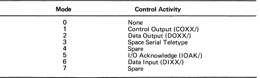
The I/O Control register modes are given in Table 4 below:
TABLE 4. BYTE I/O CONTROL MODES
BUS LINES
Mode
o
1 2
3 4
5
6 7
Control Activity
None
Control Output (COXX/) Data Output (DOXX/) Space Serial Teletype Spare
I/O Acknowledge (lOAK!) Data Input (D I XX!) Spare
The Byte I/O bus consists of the following lines: • nine input data lines
• five input control lines • nine output data lines • ten output control lines
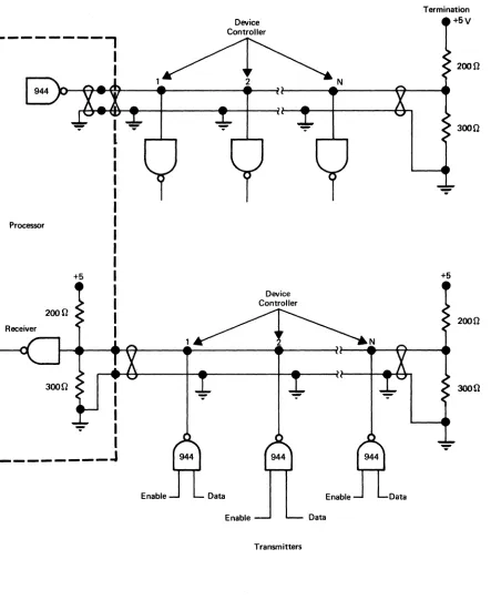
The arrangements of the input and output bus lines are shown in Figure 3. Input Lines
The nine data lines are an input to the B bus gating, and the t8 gating for the spare bit option. Three of the control lines are input to bits of file register 0 (see Table 1). The input lines are ground TRUE signals which are properly terminated at the processor. If the buss is carried out of the basic enclosure it must be terminated at the remote end also. Each peripheral device gates information onto the bus by means of open collector type 944 DTL drive circuits. Up to 15 drivers may be connected to each line.
[image:31.612.95.528.338.469.2]---,
Processor
+5
________ J
27
Enable
Device Controller
Enable
Transmitters
FIGURE 3. BUS LINES Data
Termination
+5V
200n
3000
+5
2000
3000
'"'
[
[
~
I
I
I
I
I !i
I
I
I
' I~
[
[
I
I
-I
[
[image:32.612.88.531.126.667.2]I
(
[
[
[
[
I
r
I
I
(
[
I
I
The logic levels on the twisted pairs are: One - 0 volts
Zero - +3 volts Output Lines
The nine output data lines originate with the FALSE output of the T register. The output control lines originate with the I/O Control register. If all peripheral devices on the bus are local to the enclosure, and the bus does not leave the enclosure, then the bus is standard logic levels and no DTL drivers and terminations are used. It may be necessary to repower the signals. If the bus leaves the enclosure, an I/O control board is required to provide type 944 DTL output drivers and decoding the control register. The cable length can be up to 30 feet in length and must be terminated at the remote end. Up to 15 receivers can be accommodated. The levels on the twisted pairs are:
One - 0 volts Zero - +3 volts CONTROL LINES IN
External Interrupt (EINT/): A peripheral device makes this line low to request an interrupt of the macroprogram. The program must respond with an I/O Acknowledge (mode 5) signal. This line is bit 7 of file register 0 where a I-bit indicates an external interrupt request.
I/O Reply (ERPY/): A peripheral device makes this line low in response to an I/O operation when closed loop operation is required. This line is bit 5 of file register O. The standard CIP / 2100 I/O procedures do not use this line.
I/O Request (ECIO/): A peripheral device makes this line low in order to request a concurrent data transfer. The program must respond with an I/O Acknowledge (mode 5) signal. This line is bit 3 of file register 0 where a I-bit indicates a concurrent I/O request. Device Protect (EDPR/): An external device makes this line low during a data input if
it is in a protected state thus allowing it to write into a protected area of memory when the memory protect option is installed.
Priority Return (PRRT/): This line is the return of the priority signal line. CONTROL LINES OUT
I/O Clock (KOXX/): A 50% duty cycle signal at half of the processor clock rate. Master Reset (MRES/): A low signal when either the RESET or SAVE switches on
the console is depressed.
Control Output (COXX/): A low signal which specifies that a control byte containing a device number and device order is on the output bus. The device being addressed accepts the byte.
Data Output (DOXX/): A low signal which specifies that an information byte is on the output bus for the previously addressed external device. I/O Acknowledge (lOAK./): A low signal which inputs an I/O Acknowledge byte from the external device requesting an interrupt or concurrent I/O transfer.
Data Input (DIXX/): A low signal which input an information byte from an addressed external device.
Priority Out (PROT/): This line is the start of the priority signal line. A ground on this line gives priority to the next device on the line.
PRIORITY
Devices on the byte I/O bus are assigned a priority for control of the external interrupt and I/O request lines. The priority is achieved by a signal line (PROT/ or PRRT/) which links all of the peripheral devices, not necessarily in the same order as the physical wiring of the I/O bus. A ground condition received on the priority-in signal line indicates that a device has priority if it wants to make an interrupt or I/O request. If so a ground is placed on the appropriate request signal line and not on the priority-out line. If the device does not want to make a request it places a ground on the priority-out signal line.
The processor replies to an external interrupt (EINT/) or I/O request (ECIO/) with an I/O Acknowledge which causes the device to identify itself by sending an I/O Acknowledge byte on the input bus.
CIP /2100 BYTE I/O BUS STANDARDS
The CIP / 2100 Firmware provides macro input/output instructions and a buffered concurrent I/O system. The I/O instructions perform transfers with registers and memory. The concurrent I/O performs block transfers of data which proceed concurrently with, and independent of, the macro instruction sequences being executed by the processor.
BUS MODES
In the CIP / 2100 the Byte I/O Bus modes are used as described below. Control Output
A control byte having the following format is placed on the output bus along with a mode 1
control signal (COXX/) prior to a data transfer and when some non-data transfer action is to be taken by a peripheral device.
29
_ . _ " "
-I
I
I
I, :,
I :[
I
I
-I
(
[
(
I
I
I~
r
I
I:
I
I'
The five-bit Device Number addresses one of 32 possible devices on the Byte I/O bus. The three bit Device Order specifies a particular action to be performed or indentifies the type of subsequent data transfer. The addressed device accepts the control byte and remains connected until the data transfer occurs. The non-addressed devices ignore the control byte and subsequent data transfer. The control signal is removed after four clock cycles.
Data Output
A data byte to be output is placed on the output bus along with the mode 2 control signal (DOXX/). A data byte is normally eight bits, but is expanded to nine bits if the spare memory bit option is available. The data on the bus is accepted by the addressed device and the control signal is removed after four clock cycles.
Space Serial Teletype
This mode is not associated with the Byte I/O bus, but instead controls the output state of the serial teletype interface. When the I/O Control register is in mode 3 current is removed from the output line.
I/O Acknowledge
An I/O Acknowledge byte is input from the device making an External Interrupt or Concurrent I/O Request in response to the mode 5 control signal (IOAK/). The byte has the following format:
Address
7 6 1 0
The six bit address is normally the five-bit device address with a high order O-bit. In the case of external interrupts not associated with peripheral devices a six-bit address can be used. The output flag in bit 7 is a I-bit when the device wants to perform concurrent output and is a O-bit when it wants to perform concurrent input or is requesting an external interrupt. The processor uses the address in the acknowledge byte to locate the concurrent I/O control address words or interrupt sub-routine address which are located in memory.
Data Input
A data byte to be input is placed on the input bus by the peripheral device in response to a mode 6 control signal (DIXX/). The data byte is normally eight bits, but can be expanded to nine bits if the spare memory bit option is available. The data on the input bus must be copied by some operate class command. The ninth bit of the bus can only be routed to T8 and cannot be operated on. The control signal is removed after four clock cycles.
30
CONCURRENT I/O
The concurrent I/O facility perfonns buffered block transfers of data between an external peripheral device and memory. The maximum total transfer rate is 50,000 bytes per second. Address control for each device is performed by two 16-bit addresses located in core memory. The first address specifies the current memory address and the other specifies the last address of the data block.
The peripheral device is placed in a concurrent input or output mode by a control byte sent to the device. The device requests data transfers by the I/O Request line. When the processor recognizes the request it performs the transfer and increments the current address. When the current address eqUfls the end address + 1, the processor sends a control byte to the device to stop the concurrent operation.
Concurrent Data Input Procedures
a. Device wanting to input data to memory and having highest priority grounds the I/O request control line.
b. When the processor's microprogram senses an I/O Request at bit 3 of file register
o
it grounds the I/O Acknowledge.c. Device sending I/O Request senses I/O Acknowledge and places an I/O Acknowledge byte, with and O-bit in bit 7, on the input bus.
d. Processor's microprogram inputs acknowledge byte and removes I/O acknowledge signal.
e. Device senses removal of the I/O Acknowledge and removes T '0 Request signal.
f. Processor's microprogram grounds data input signal. g. Device gates input data byte onto input bus.
h. Processor's microprogram inputs data byte, removes data input signal, and stores data in memory at address determined by address control words in memory. Concurrent Data Output Procedures
31
a. Device wanting to receive data from memory and having the highest priority grounds the I/O Request control line.
b. When the processor's microprogram senses the I/O request at bit 3 of file register
o
it grounds the I/O Acknowledge.c. Device sending I/O request senses I/O Acknowledge and places an I/O Acknowiedge byte with a i -bIt In bIt' / , on the input bus.
d. Processor's microprogram inputs address byte and removes I/O Acknowledge signal.
e. Device senses removal of the I/O Acknowledge and removes I/O Request signal.
I
"
I', :
I
I
I
I
~
lI;
[
I
I
-I.
[
(
('
I
I
[
[
I:
[
"I"'
", "
,
I
I
I
I
I
I:
f. Processor's microprogram places accessed data on output bus and sends Data Output signal. Memory location of data is determined by address words in memory.
INTERRUPT
The Interrupt facility makes use of a single interrupt line which a priority interrupt channel or an End-of-Block interrupt from an I/O Device may activate. When the processor recognizes the interrupt request (between macro instructions), the interrupting device identifies itself. In core mem0ry, the address of the interrupt handling sub-routine is kept at a fixed address. The device identification, along with a displacement, is used to refer to that fixed address, and then a Return Jump is activated into the sub-routine.
Interrupt Procedures
a. Device wanting to interrupt and having highest priority grounds External Interrupt (EINT /) control line.
b. When the processor's microprogram senses an External Interrupt request at bit 7 of file register 0 it grounds the I/O Acknowledge.
c. Device sending External Interrupt senses I/O Acknowledge and places an I/O Acknowledge byte on the input bus.
d. Processor's microprogram inputs acknowledge byte and removes I/O Acknowledge signal.
e. Device senses removal of I/O Acknowledge and removes External Interrupt and the acknowledge byte.
f. Processor's microprogram uses acknowledge byte to determine interrupting device and processes interrupt accordingly.