© 2019, IRJET | Impact Factor value: 7.211 | ISO 9001:2008 Certified Journal
| Page 3855
A DC-DC Converter with High Voltage Gain for Motor Applications Using
Fuel Cell
Dinakaran.K.P
1, Manimurugan.M
2, Deepak.M
3, Naveen.D
4, Praveen Kumar.C
5,
Praveen Kumar.K
61
Assistant Professor,Dept. of Electrical& Electronic Engineering,Panimalar Institute of Technology,TN,India.
2
Assistant Professor,Dept. of Electrical& Electronic Engineering,Panimalar Institute of Technology,TN,India.
3
UG,Dept. of Electrical& Electronic Engineering,Panimalar Institute of Technology,TN,India.
4
UG,Dept. of Electrical& Electronic Engineering,Panimalar Institute of Technology,TN,India.
5
UG,Dept. of Electrical& Electronic Engineering,Panimalar Institute of Technology,TN,India.
6
UG,Dept. of Electrical& Electronic Engineering,Panimalar Institute of Technology,TN,India.
---***---Abstract -
In a fuel cell vehicle, the output voltage of the
fuel cell source is typically much lower than the voltage required by the system. A new DC-DC boost converter with a ideal input range and high voltage gain is proposed to act as the required power interface, which reduces the voltage stress across the system. The converter was measured as 95.01% efficiency. A DC motor is connected across the output side and closed loop is performed. Simulation is performed using MATLAB software and simulation result are shown. A simple prototype is shown in open loop .It is mainly used for motor applications and in industrial areas .The output of the motor is connected to PI controller and closed is performed .The closed loop is performed and the motor load does not vary in speed Fuel cell is used in project because it is renewable form of energy .The fuel cell uses hydrogen as fuel which is easily available and the byproduct of the Fuel cell is water .It is far convenient and does not wide open to environment .The usage of Fuel cell in the project opens wide range usage of fuel cell .
Key Words: Boost DC-DC converter, Fuel cell Vehicles, High voltage-gain, Switched-capacitor, Wide input range.
1.INTRODUCTION
As non-renewable resources such as oil, gas and coal become scarce, more and more research is focused on the problem of high energy usage and society’s dependence on fossil fuels. Additionally, the number of automobiles continues to increase in most countries, causing a significant rise in air pollution. Vehicles powered by fuel cell sources may help to reduce transport’s dependence on oil, and reduce polluting emissions. The fuel cells can utilize hydrogen or natural gas, to achieve a high energy density and can potentially generate “clean” electricity with high efficiency.
However, unlike batteries which have a fairly constant output voltage, the output voltage of fuel cells drops significantly with an increase of output current. Hence, a step-up DC-DC converter with a wide range of voltage-gain is
essential to interface between the low voltage fuel-cell source and the high voltage DC bus of the motor drive inverter. The conventional DC-DC Boost converters one of the most commonly used topologies for stepping up voltage. In theory, when the duty cycle approaches unity, the conventional boost converter can achieve a high voltage gain. However, it is difficult to implement a high voltage gain (e.g. more than 6), due to the existence of parasitic elements (stray inductance, capacitance) and the extreme duty cycle required. In addition, the power semiconductors suffer from a high voltage stress - the DC bus voltage. In order to obtain a DC-DC Boost converter with a high voltage gain and a low voltage stress, many different topologies have been proposed by researchers.
These converters can be divided into two types: isolated and non-isolated converters. Isolated converters are widely used in many applications, and an arbitrarily high voltage-gain can be theoretically achieved by increasing the turns ratio of the transformer employed. However, there are many situations where galvanic isolation is unnecessary, and the snubber circuit required in an isolated topology will increase the complexity of the converter design. Compared with isolated converters, the cost and magnetic losses of non-isolated converters are lower. A high voltage-gain can be achieved by introducing a coupled inductor to topology, and the converter can maintain a low device voltage stress. However, a large number of inductors is required leading to an increased volume, a higher cost, and a reduced efficiency. Non-coupled inductor-based converters can also be used to obtain a high voltage-gain reducing the number of magnetic devices.
© 2019, IRJET | Impact Factor value: 7.211 | ISO 9001:2008 Certified Journal
| Page 3856
stress across the power semiconductors can be reduced byhalf, and the voltages across the output capacitors can also balance themselves naturally.
However, the power switches may see a large voltage spike as a result of the leakage inductance of the circuit. The switched-capacitor circuit was studied in : it achieves flexible voltage regulation by combining it with other DC-DC converters, however the difference in potential between the ground points of the input voltage source side and the load side is a high frequency PWM voltage, because instead of a common ground structure, there is a diode located between the ground points of the input voltage source side and the load side. As a result, it may introduce issues associated with du/dt and these may limit its applications. The Z source DC-DC Boost converter has the potential for a high voltage gain. A Z source DC-DC converter with a cascaded switched-capacitor has been presented in. This topology can improve the voltage gain of the Z source DC-DC Boost converter by using the voltage multiplier function of the switched-capacitor. However, the drawbacks of the converter are obvious, such as the penalty of the discontinuous input current and the different ground points between the input voltage source side and the load side. Moreover, the power semiconductors will see a high voltage stress when the duty cycle approaches zero.
In a similar way, switched-inductor (SL) techniques can also be used in dc-dc converters to achieve a high voltage gain as presented in, and, but they often need large numbers of inductors. Therefore, the volume and cost of these converters will be increased. To address these issues, a new non-isolated high ratio step-up dc-dc converter is proposed in this Thesis, which has the following features:
1) It reduces the voltage stress across the power devices and has a common ground between the input and output sides. 2) The two power switches turn on and off simultaneously. As a result, the control of the converter is simple, and power switches with low on-state resistance can be employed. 3) The system operates with a high voltage gain and a wide input voltage range and does not use any extreme values for its duty cycle.
This paper is organized as follows: In Section II, the configuration and operating principles of the proposed converter are presented. The voltage gain is analyzed in Section III. In Section IV, the voltage and current stresses are calculated. The design of the components is presented in Section V and in Section VI, the dynamic modeling is established. Experimental results and analysis are presented in Section VII to validate the features of the proposed converter.
2. EXISTING METHODOLGY
Since the voltage of the fuel cell source is very low and the high voltage DC bus of the motor drive inverter. The existing DC-DC converter produces variable output voltage with respect to low voltage input from fuel cell and it cannot be used for motor loads. The increasing load drops the efficiency
of the fuel cell. It has no common ground, high voltage stress. The Existing or proposed converter uses only resistive load and it.
3.
OPERATING PRINCIPAL OF PROPOSED
[image:2.595.312.543.133.272.2]CONVERTER
Fig -1: Block Diagram of Proposed System
3.1 Configuration of the proposed converter
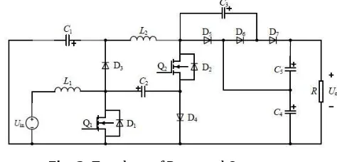
The high voltage gain DC-DC Boost converter is shown in Fig. 1. It comprises two active power switches (Q1 and Q2), five power diodes (D3-D7), two inductors (L1 and L2) and five capacitors (C1-C5). The fuel-cell source Uin and the inductor L1 are connected in series to charge capacitors C1 and C2 in parallel.
Inductor L2 is another energy storage component which is used to realize a high voltage gain. The ladder type voltage multiplier (capacitors C3-C5 and diodes D5-D7) can improve the voltage-gain further and reduces the voltage stress across the power semiconductors on the high voltage side.
Fig -2: Topology of Proposed Converter
3.2 Operating principles of the proposed
converter
The gate signals of the two power switches (Q1, Q2) are identical - Q1 and Q2 are turned on and off simultaneously. Therefore, there are two switching states in each switching period, which are shown in Fig. 3.
Switching state 1. As shown in Fig. 3(a), Q1 and Q2 turn on, L1 is charged by the DC source Uin (i.e. Uin-L1-Q1), and L2 is charged by C1 and C2 in series (i.e. C1-L2-Q2-C2-Q1). Meanwhile, C3 is charged by C2 and C4 in series (i.e. C4-D6-C3-Q2-C2-Q1).
[image:2.595.315.552.451.565.2]© 2019, IRJET | Impact Factor value: 7.211 | ISO 9001:2008 Certified Journal
| Page 3857
the DC source, L1, L2, and C3 (i.e.Uin-L1-D3-L2-C3-D7-C5-C4), as well as through the load R. The output-voltage Uo is equal to the total voltages across C4 and C5.
Fig -3(a): Switching states of the proposed converter - Switching state 1.
Fig -3(b): Switching states of the proposed converter - Switching state 2.
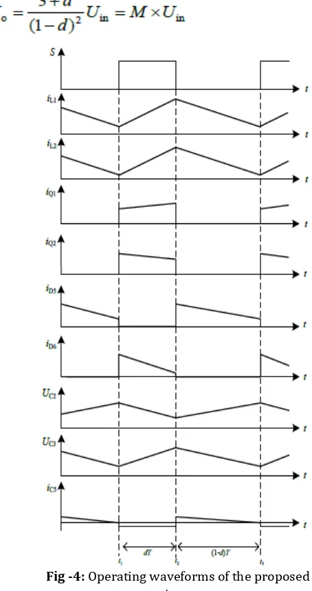
According to the key operating waveforms of the proposed converter shown in Fig. 4, the inductor currents iL1 and iL2 have the same energy transfer process. When S=1, power switches Q1, Q2 and diode D6 are turned on. The current iQ1 increases linearly while iQ2 and iD6 decreases linearly. The output capacitor current iC5 is negative which means C5 is discharged. When S=0, power switches Q1, Q2 and diode D6 are turned off. The currents iD5 and iC5 decrease linearly. The capacitor voltage fluctuations reflect the charging and discharging processes. It can be seen from the capacitor voltages UC2 and UC3 that capacitors C2 and C3 have the opposite charging and discharging states.
4. STEADY-STATE ANALYSIS
If the switching period for the power switches is T, then, dT is the on-state period, and (1-d) T is the off-state period, where d is the duty cycle of the power switches. It is assumed that the capacitor voltage and the inductor current are constant during each switching period, and the forward voltage drop and the on-state resistance of the power semiconductors are ignored.
The voltage relationship between the output and capacitor voltages can be found, in terms of the two switching states which are shown in Fig. 3:
[image:3.595.42.286.149.253.2]As a result, the output voltage Uo can be obtained from above equations as follows:
Fig -4: Operating waveforms of the proposed converter
[image:3.595.322.549.197.627.2] [image:3.595.41.278.290.393.2]© 2019, IRJET | Impact Factor value: 7.211 | ISO 9001:2008 Certified Journal
| Page 3858
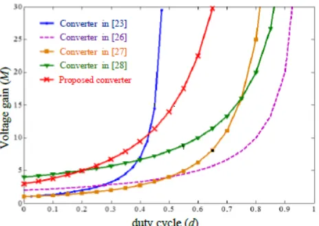
will be analyzed in Table I. Considering the voltage gain, theefficiency and the common ground together, the proposed converter in this paper has the advantages of a high and wide voltage gain range, an acceptable conversion efficiency, and a common ground.
Fig -5: Comparisons of voltage gain as a function of the duty cycle for different converter topologies.
5. SIMULATION RESULTS
6. HARDWARE RESULTS
7. CONCLUSIONS
A high voltage gain DC-DC Boost converter with a wide input range, continuous input current and common ground points between the input side and the load side has been proposed in this paper. The voltage stress across the main power switches is lower than half of the output voltage. In addition, the proposed converter can keep the output voltage at 400V using a voltage control loop, when the input voltage changes from 80V to 40V. Therefore, it is suitable for the power interface between a fuel cell source and the DC bus for the motor drive in fuel cell vehicles.
REFERENCES
[1] B. Zeng, J. Zhang, X. Yang, J. Wang, J. Dong, and Y. Zhang,
“Integrated planning for transition to low-carbon distribution system with renewable energy generation and demand response,” IEEE Trans. Power Syst., vol. 29, no. 3, pp. 1153–1165, May 2014 .
[2] H. Rudnick, R. Palma-Behnke, A. Rudnick, and C.
Benavides, “Restless Waters: Fossil Fuel Emissions Conditioning a Reduction in Hydroelectric Resources in Chile,” IEEE Power Energy Mag., vol. 12, no. 5, pp. 50-60, Aug. 2014.
[3] A. Emadi, and S. S. Williamson, “Fuel Cell Vehicles:
[image:4.595.50.282.173.337.2]© 2019, IRJET | Impact Factor value: 7.211 | ISO 9001:2008 Certified Journal
| Page 3859
[4] M. Shen, A. Joseph, J. Wang, F.Z. Peng, and D. J. Adams,
“Comparison of Traditional Inverters and Z-Source Inverter for Fuel Cell Vehicles,” IEEE Trans. Power Electron., vol. 22, no. 4, pp. 1453–1463, Jul. 2007.
[5] Y. Zhang, C. Fu, M. Sumner, and P. Wang, “A Wide
Input-Voltage Range Quasi-ZSource Boost DC-DC Converter with High Voltage-Gain for Fuel Cell Vehicles.”IEEE Trans. Ind. Electron., in press.
[6] G. Dotelli, R. Ferrero, P. G. Stampino, S. Latorrata, and S.
Toscani, “PEM fuel cell drying and flooding diagnosis with signals injected by a power converter,” IEEE Trans. Instrum. Meas., vol. 64, no. 8, pp. 2064–2071, Aug. 2015.
[7] F. L. Tofoli, D. de Castro Pereira, W. J. de Paula, and D. de
Sousa Oliveira Junior, “Survey on non-isolated high-voltage step-up DC-DC ´ topologies based on the boost converter,” IET Power Electron., vol. 8, no. 10, pp. 2044– 2057, 2015.
[8] J. H. Lee, T. J. Liang, and J. F. Chen, “Isolated
coupled-inductor integrated DC-DC converter with nondissipative snubber for solar energy applications,” IEEE Trans. Ind. Electron., vol. 61, no. 7, pp. 3337–3348, Jul. 2014.
[9] W. H. Li, X. N. He, “Review of Nonisolated High-Step-Up
DC/DC Converters in Photovoltaic Grid-Connected Applications,” IEEE Trans. Ind. Electron., vol. 58,no. 4, pp. 1239–1250, Apr. 2011.
[10]P. Sadat, and K. Abbaszadeh, “A Single-Switch High
Step-Up DC–DC Converter Based on Quadratic Boost,”IEEE Trans.Ind. Electron., vol. 63, no.12, pp.2959-2968. Dec.2016.
[11]H. Choi, M. Ciobotaru, M. Jang, and V. G. Agelidis,
“Performance of medium-voltage DC-bus PV system architecture utilizing high-gain DCDC converter,” IEEE Trans. Sustain. Energy, vol. 6, no. 2, pp. 464–473, Apr. 2015.
[12]A. Ioinovici, “Switched-capacitor power electronics
circuits,” IEEE Circuits Syst. Mag., vol. 1, no. 4, pp. 37-42, Sep. 2001.
[13]G. Wu, X. Ruan, and Z. Ye, “Nonisolated high step-up
dc-dc converters adopting switched-capacitor cell,” IEEE Trans. Ind. Electron., vol. 61, no. 1, pp. 383-393, Jan. 2015.
[14]Y. Tang, T. Wang, and Y. He, “A switched-capacitor-based
active-network converter with high voltage gain,” IEEE Trans. Power Electron., vol. 29, no. 6, pp. 2959–2968, Jun. 2014.
[15]B. Axelrod, Y. Berkovich, and A. Ioinovici,
“Transformerless DC-DC converters with a very high DC line-to-load voltage ratio,” J. Circuits, Syst. Comput., vol. 13, no. 3, pp. 467-475, Jun. 2004.
[16]G. Zhang, B. Zhang, Z. Li, D. Qiu, L. Yang, and W. A.
Halang. “A 3-Z-network boost converter,” IEEE Trans. Ind. Electron., vol. 62, no. 1, pp. 278-288, Jan. 2015.
[17]M. Zhu, K. Yu and F. L. Luo “Switched-inductor Z-source
inverter,” IEEE Trans. Power Electron., vol. 25, no. 8, pp. 2150-2158, Aug. 2010.
[18]M. Prudente, L. L. Pfitscher, G. Emmendoerfer, E. F.
Romaneli and R. Gules, “Voltage Multiplier Cells Applied to Non-Isolated DC–DC Converters,” IEEE Trans. Power Electron., vol. 23, no. 2, pp. 871-887, Mar. 2008.
[19]Y. R. Novaes, A. Rufer, and I. Barbi, “A new quadratic,
three-level, dc/dc converter suitable for fuel cell applications,” in Proc. Power Convers. Conf., Nagoya, Japan, 2007, pp. 601–607.
[20]C. T. Pan, C. F. Chuang, and C. C. Chu, “A novel
transformer-less adaptable voltage quadrupler DC converter with low switch voltage stress,” IEEE Trans. Power Electron., vol. 29, no. 9, pp. 4787–4796, Sep. 2014.
[21]O. Cornea, GD. Andreescu, N. Muntean, and D. Hulea,