Interleaved Switched-Capacitor Bidirectional DC-DC Converter
with Wide Voltage-Gain Range for Energy Storage Systems
Yun Zhang,
Member
,
IEEE
, Yongping Gao, Jing Li,
Member
,
IEEE
, Mark Sumner,
Senior
Member
,
IEEE
Abstract²In this paper, an interleaved switched-capacitor
bidirectional DC-DC converter with a high step-up/step-down voltage gain is proposed. The interleaved structure is adopted in the low-voltage side of this converter to reduce the ripple of the current through the low-voltage side, and the series-connected structure is adopted in the high-voltage side to achieve the high step-up/step-down voltage gain. In addition, the bidirectional synchronous rectification operations are carried out without requiring any extra hardware, and the efficiency of the converter is improved. Furthermore, the operating principles, voltage and current stresses, and current ripple characteristics of the converter are analyzed. Finally, a 1kW prototype has been developed which verifies a wide voltage-gain range of this converter between the variable low-voltage side (50V-120V) and the constant high-voltage side (400V). The maximum efficiency of the converter is 95.21% in the step-up mode and 95.30% in the step-down mode. The experimental results also validate the feasibility and the effectiveness of the proposed topology.
Index Terms²Bidirectional DC-DC converter, Interleaved, Switched-capacitor, Synchronous rectification, Wide-voltage-gain range
I. INTRODUCTION
With the aggravation of the global energy crisis and the deterioration of the environment pollution, the renewable energy systems become very important in the world [1] , [2] . However, the renewable energy systems, including photo-voltaic systems and wind-power generating systems, cannot provide a stable power and supply enough instantaneous power when the load power suddenly increases. Energy storage systems, which are used to compensate the power fluctuation between the power generation side and the load side, play an important role in renewable energy power systems [3] , [4] . A bidirectional DC±DC converter is a key device for interfacing an energy storage element such as a battery pack or a super-capacitor pack, with a DC bus [5] , [6] . The voltage of a storage battery is typically 48V or lower, while the voltage of a DC bus is 400V or higher [7] . Thus, a bidirectional DC±DC converter with a wide voltage-gain range is desired for energy storage systems to connect a low-voltage battery with a high-voltage DC bus.
There are two different types of bidirectional DC-DC converters in different applications, which include the isolated converters and non-isolated converters. The isolated converters include the Flyback, the Forward-Flyback, the half-bridge and the full-bridge. High voltage-gain is obtained by adjusting the turns ratio of the high frequency transformer. However, the leakage inductance of the transformer results in high voltage spikes on semiconductors. In order to reduce the voltage stress
caused by the leakage inductance, a full bridge bidirectional DC-DC converter with a Flyback snubber circuit [8] and a bidirectional DC-DC converter with an active clamp circuit [9] were proposed. Although the energy of the leakage inductor can be recycled, more additional circuits are required. Besides, when the input and the output voltages cannot match the turns ratio of the transformer, the switching loss will increase dramatically [10] .
power semiconductors. The switched-capacitor converter structures and control strategies are simple and easy to expand. Different charging and discharging paths of the capacitors transfer energy to either the low-voltage or the high-voltage side to achieve a high voltage gain. Single capacitor bidirectional switched-capacitor converters were proposed in [22] , [23] , but the converter¶V efficiency is low. To reduce the input current ripple, interleaved switched-capacitor converters have been proposed in [24] -[27] . However, the converter in [24] needs more components, and the inductor currents of the converter in [25] are unbalanced when Db is not equal to 2Da. Although the
bidirectional DC-DC converters in [26] , and [27] just need four semiconductors, the maximum voltage stress of the converter in [26] is that of the high voltage side, and the maximum voltage stress of the converter in [27] is higher than that of the high voltage side. The bidirectional converters in [28] , and [29] only require three semiconductors. But their voltage-gain ranges are still small. In addition, the low-voltage and high-voltage side grounds of these converter are connected by a power semiconductor or an inductor, which will also cause extra EMI problems. Finally, the high voltage-gain converter in [30] needs more power components and fails to achieve bidirectional power flows. In addition, the balanced inductor currents just can be achieved when the number of the voltage multiplier stages is odd. The converter in [31] suffers from the huge current ripple in the low-voltage side.
These non-isolated bidirectional DC-DC converters referred above cannot simultaneously achieve the low current ripple, the low voltage stress of power semiconductors and the wide voltage-gain range. In order to solve this problem, an interleaved switched-capacitor bidirectional DC-DC converter is proposed in this paper. Comparing with the conventional two-phase interleaved bidirectional DC-DC converter and the bidirectional three-level DC-DC converter, the proposed converter has advantages including low current ripple, low voltage-stress of power semiconductors and wide voltage-gain range. In addition, the connection between the low-voltage and the high-voltage side grounds of the proposed converter is a capacitor rather than a power semiconductor. To achieve a high step-up gain, the capacitors are charged in parallel and discharged in series in the step-up mode. Opposite to the step-up mode, the high step-down ratio can also be obtained because two capacitors are charged in series and discharged in parallel. Furthermore, the capacitor voltage of the proposed converter is half of the high-voltage side voltage, and the efficiency is improved by synchronous rectification operation. This paper is organized as follows. In Section II, the topology of the interleaved switched-capacitor bidirectional DC-DC converter is presented. In Section III, the operating principles of the proposed converter are analyzed in detail. The steady-state characteristics of the converter are analyzed in Section IV and experimental results are analyzed in Section V.
II. THE PROPOSED CONVERTER
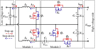
The proposed interleaved switched-capacitor bidirectional DC-DC Converter is shown in Fig. 1. This converter is composed of four modules. Clow is the energy storage/filter
capacitor of the low-voltage side. Module 1 includes power
semiconductors Q1, Q2, and energy storage/filter inductors L1,
L2. In addition, L1-Q1 and L2-Q2 form the parallel structure of the
low-voltage side. Module 2 is a switched-capacitor network, including switched-capacitor units C1-Q3, C2-Q4 and C3-Q5. The
interleaved structure is used in the low-voltage side of this converter. In this case, the duty cycles of Q1 and Q2 are the same,
and the phase difference between the gate signals S1 and S2 is
180°. The low-voltage side, Module 1, Module 2 and the high-voltage side form the bidirectional DC-DC converter with the structure of the low-voltage-side in parallel and the high-voltage-side in series.
-+
Clow Ulow
C1
UC1
-+
-+ C3 UC3
-+ C2 UC2
-+
Uhigh
S1 Q1
S2 Q2
S4 Q4
S3 Q3
S5 Q5 L1
L2 iL1
iL2 Step-down
Step-up
Module 1 Module 2
ilow ihigh
H
igh
-vol
ta
ge
s
ide
L
ow
-vol
ta
ge
s
[image:2.595.330.525.217.317.2]ide
Fig. 1 The proposed topology of the interleaved switched-capacitor bidirectional DC-DC Converter.
III. OPERATING PRINCIPLES
To simplify the steady-state characteristics analysis of the proposed converter, several reasonable assumptions about the operating conditions are made as follows: (a) all the power semiconductors and energy storage components of the converter are treated as ideal ones, and the converter operates in the continuous conduction mode (CCM); (b) all the capacitances are large enough that each capacitor voltage is considered as constant in each switching period.
A. Step-Up Mode
When the energy flows from the low-voltage side to the high-voltage side, the output voltage Uhigh is stepped up from
Ulow by controlling the power semiconductors of Q1, and Q2, and
the anti-parallel diodes of Q3, Q4 and Q5. The relationship
between d1 and d2 can be written as d1=d2=dBoost, where d1 and
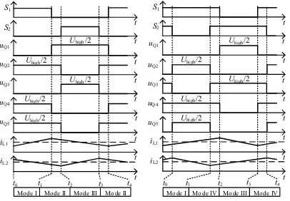
d2 are the duty cycles of Q1 and Q2 respectively. Fig. 2 shows the
typical waveforms in the step-up mode, and Fig. 3 shows the current flow path of the proposed converter.
Mode I: The power semiconductor Q1 is turned on and Q2 is
turned off. The anti-parallel diode of Q3 is turned on, while the
anti-parallel diodes of Q4 and Q5 are turned off. The current flow
path of the proposed converter is illustrated in Fig. 3(a). The energy is transferred from the DC source Ulow to the inductor L1.
Meantime, C1 is being charged by inductor L2, while C2 and C3
are discharging. C2 and C3 are connected in series to provide
energy for the load in the high voltage side.
Mode II: The power semiconductors Q1 and Q2 are turned off.
The anti-parallel diodes of Q3 and Q4 are turned on, while the
anti-parallel diode of Q5 is turned off. The current flow path of
the proposed converter is given in Fig. 3(b). Inductors L1 and L2
are discharging. Meantime, C1 is charging from inductor L2,
while C3 is discharging. The DC source Ulow, L1 and C3 output
energy to the load.
is turned on. The anti-parallel diode of Q3 is turned off, while
the anti-parallel diodes of Q4 and Q5 are turned on. The current
flow path of the proposed converter is shown in Fig. 3(c). Inductor L1 is discharging, while L2 is charged by the DC source.
Meantime, C3 is charged by C1, while C2 is charged by inductor
L1. The DC source Ulow, L1 and C1 output energy to the load.
Mode IV: Power semiconductors Q1 and Q2 are turned on.
The anti-parallel diodes of Q3 and Q4 are turned off, while the
anti-parallel diode of Q5 is turned on. The current flow path of
the proposed converter is displayed in Fig. 3(d). Inductors L1
and L2 are charged by the DC source Ulow in parallel. Meantime,
C1 and C2 are discharging in series to provide energy for the
load.
S2
uQ2 S1
t
t
t
t uQ1
t
t
t
t uQ3
uQ4
uQ5
iL1
iL2
Uhigh/2
Uhigh/2
Uhigh/2 Uhigh/2
Uhigh/2
t S1
S2
uQ1
uQ2
uQ3
uQ4
uQ5
iL1
iL2
Uhigh/2
Uhigh/2
Uhigh/2 Uhigh/2
Uhigh/2
t0 t1 t2 t3 t4 t t
t
t
t
t
t
t
t
Mo de I Mo de II Mo de III Mo de II
t0 t1 t2 t3 t4
Mo de I Mo de IV Mo de III Mo de IV (a) (b)
Fig. 2 Typical waveforms of the proposed converter in the step-up mode. (a) 0<dBoost<0.5. (b) dBoost<1.
-+
Clow Ulow
C1
UC1
-+
-+ C3 UC3
-+ C2 UC2
-+
Uhigh
S1 Q1
S2 Q2 S4
Q4
S3 Q3
S5 Q5 L1
L2 iL1
iL2
-+uL1
-+uL2
ilow ihigh
iC1
iC2
iC3
(a)
-+
Clow Ulow
C1
UC1
-+
-+ C3 UC3
-+ C2 UC2
-+
Uhigh
S1 Q1
S2 Q2 S4
Q4
S3 Q3
S5 Q5 L1
L2
-+
-+
ilow iL1 ihigh
iL2 uL1
uL2 i
C1
iC2
iC3
(b)
-+
Clow Ulow
C1
UC1
-+
-+ C3 UC3
-+ C2 UC2
-+
Uhigh
S1 Q1
S2 Q2
S4 Q4
S3 Q3
S5 L1
L2
-+
-+
Q5
ilow iL1 ihigh
iL2 uL1
uL2 i
C1
iC2
iC3
(c)
iL1
iL2 uL1
uL2 i
C1
iC2
iC3
-+ Clow Ulow
C1
UC1
-+
-+ C3 UC3
-+ C2 UC2
-+
Uhigh
S1 Q1
S2 Q2
S4 Q4
S3 Q3
S5 L1
L2
-+
-+
Q5
ilow ihigh
(d)
Fig. 3 Current flow path of the proposed converter in the step-up mode. (a) Mode I S1S2=10. (b) Mode II S1S2=00. (c) Mode III S1S2=01.
(d) Mode IV S1S2=11.
B. Step-Down Mode
When energy flows from the high-voltage side to the low-voltage side, the output voltage Ulowis stepped down from
Uhigh by controlling the power semiconductors Q3, Q4 and Q5,
and the anti-parallel diodes of Q1 and Q2. The relationship
between d3 and d4 can be written as d3=d4=dBuck, where d3 and d4
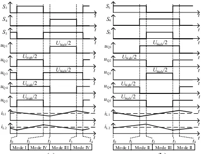
are the duty cycles of Q3 and Q4 respectively. Fig. 4 shows the
typical waveforms in the step-down mode, and Fig. 5 shows the current flow path of the proposed converter.
Mode I: The power semiconductor Q3 is turned on, while Q4
and Q5 are turned off. The anti-parallel diode of Q1 is turned on,
and the anti-parallel diode of Q2 is turned off. The current flow
path of the proposed converter is shown in Fig. 5(a). C2 and C3
are charged by the DC source Uhigh in series. Meantime,
inductors L1, L2 and C1 are discharging to provide energy for the
load in the low voltage side.
Mode II: Power semiconductors Q3 and Q4 are turned on,
while Q5 is turned off. The anti-parallel diodes of Q1 and Q2 are
turned off. The current flow path is shown in Fig. 5(b). C1 is
discharging to transfer energy to inductor L2, and
simultaneously outputting energy to the load. Meantime, the DC source Uhigh charges L1 and C3, and simultaneously outputs
energy to the load. In addition, C2 is discharging to supply
energy to L1 and the load.
Mode III: The power semiconductor Q3 is turned off, while
Q4 and Q5 are turned on. The anti-parallel diode of Q1 is turned
off, and the anti-parallel diode of Q2 is turned on. The current
flow path of the proposed converter is shown in Fig. 5(c). Inductor L2 is discharging to provide energy for the load.
Meantime, the DC source Uhigh charges L1 and C1, and
simultaneously provide energy for the load. In addition, C2 is
discharging to supply energy to L1 and the load, and C3 is
discharging to output energy to C1.
Mode IV: Power semiconductors Q3 and Q4 are turned off,
while Q5 is turned on. The anti-parallel diodes of Q1 and Q2 are
turned on. The current low path of the proposed converter is shown in Fig. 5(d). L1 and L2 are discharging to provide energy
for the load in parallel. Meantime, the DC source Uhigh charges
[image:3.595.333.519.85.193.2] [image:3.595.68.271.237.378.2]uQ2 t
t uQ1
t
t
t
t uQ3
uQ4
uQ5
t t0
iL1
iL2
Uhigh/2
Uhigh/2
Uhigh/2
Uhigh/2
Uhigh/2
t2
t1 t3 t4
uQ1
uQ2
uQ3
uQ4
uQ5
iL1
iL2
Uhigh/2
Uhigh/2
Uhigh/2 Uhigh/2
Uhigh/2
t0 t1 t2 t3 t4t t
t
t
t
t
t S4
S3
t t
S5
t S4
S3
t t
S5
t
[image:4.595.317.532.86.417.2]Mo de I Mo de IV Mo de III Mo de IV Mo de I Mo de II Mo de III Mo de II (a) (b)
Fig. 4 Typical waveforms of the proposed converter in the step-down mode. (a) 0<dBuck<0.5. (b) dBuck<1.
-+
Clow Ulow
C1
UC1
-+
-+ C3 UC3
-+ C2 UC2
-+
Uhigh
S1 Q1
S2 Q2 S4
Q4
S3 Q3
S5 Q5 L1
L2
- +
- +
ilow iL1 ihigh
iL2 uL1
uL2 i
C1
iC2
iC3
(a)
-+
Clow Ulow
C1
UC1
-+
-+ C3 UC3
-+ C2 UC2
-+
Uhigh
S1 Q1
S2 Q2 S4
Q4
S3 Q3
S5 Q5 L1
L2
- +
- +
ilow iL1 ihigh
iL2 uL1
uL2 i
C1
iC2
iC3
(b)
-+
Clow Ulow
C1
UC1
-+
-+ C3 UC3
-+ C2 UC2
-+
Uhigh
S1 Q1
S2 Q2
S4 Q4
S3 Q3
S5 L1
L2
- +
- +
Q5
ilow iL1 ihigh
iL2 uL1
uL2 i
C1
iC2
iC3
(c)
iL1
iL2 uL1
uL2 i
C1
iC2
iC3
-+ Clow Ulow
C1
UC1
-+
-+ C3 UC3
-+ C2 UC2
-+
Uhigh
S1 Q1
S2 Q2
S4 Q4
S3 Q3
S5 L1
L2
- +
- +
Q5
ilow ihigh
[image:4.595.67.269.88.243.2](d)
Fig. 5 Current flow path of the proposed converter in the step-down mode. (a) Mode I S3S4S5=100. (b) Mode II S3S4S5=110. (c) Mode III S3S4S5=011. (d) Mode IV S3S4S5=001.
C. Synchronous rectification operation
S1
S2
S3
S4
S5
t
t
t
t
t td
td
td
td
td td
S1
S2
S3
S4
S5
t
t
t
t
t td
td
td td
(a) (b)
-+
Clow
Ulow
C1
UC1
-+
-+ C3 UC3
-+ C2 UC2
-+
Uhigh
S1 Q1
S2 Q2
S4 Q4
S3 Q3
S5
Q5
L1
L2
iL1
iL2
step-up
-+uL1
-+uL2
without current with current during dead time
(c)
-+
Clow
Ulow
C1
UC1
-+
-+ C3 UC3
-+ C2 UC2
-+
Uhigh
S1 Q1
S2 Q2
S4 Q4
S3 Q3
S5
Q5
L1
L2
iL1
iL2
step-down
+
-uL1
+
-uL2
without current with current during dead time
[image:4.595.72.265.269.720.2](d)
Fig. 6 Synchronous rectification operating principle of the proposed bidirectional converter. (a) Gate signals and the dead time in the step-up mode (left). (b) Gate signals and the dead time in the step-down mode (right). (c) Current flow path in the step-up mode. (d) Current flow path in the step-down mode.
As shown in Fig. 1, if the currents of the proposed interleaved switched-capacitor bidirectional converter flow into the corresponding anti-parallel diodes, it will result in the lower efficiency, as well as lower utilization of the power semiconductors. Therefore, a high step-up/step-down ratio switched-capacitor bidirectional DC-DC converter with synchronous rectification is proposed further in this paper.
The synchronous rectification operating principle of the switched-capacitor bidirectional converter is shown in Fig. 6. In the step-up mode, the main power semiconductors Q1 and Q2
switch according to gate signals S1 and S2 shown in Fig. 6(a).
During the dead time td, the current has to fully flow into the
corresponding anti-parallel diodes of Q3, Q4 and Q5. Otherwise,
the current may flow into the controlled power semiconductors
Q3, Q4 and Q5 due to their lower on-resistances and on-state
voltage drops, as shown in Fig. 6(c), by means of the gate signals S3, S4 and S5 shown in Fig. 6(a). Similarly, in the
step-down mode, the main power semiconductors Q3, Q4 and Q5
switch according to gate signals S3, S4 and S5 shown in Fig. 6(b).
During the dead time td, the current also has to fully flow into the
anti-parallel diodes of Q1 and Q2. Otherwise, according to the
gate signals S1 and S2 shown in Fig. 6(b), the current flows into
the controlled power semiconductors Q1 and Q2, as shown in Fig.
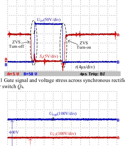
Furthermore, the forward voltage drops of the anti-parallel diodes are close to zero. As a result, the controlled MOSFETs of the slave active power semiconductors can be turned on and turned off with ZVS, and the efficiency of the converter is further improved.
D. Control strategy of bidirectional power flow
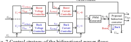
Based on the operating principles above, the bidirectional power flow control strategy can be achieved as shown in Fig. 7. The voltages Uhigh and Ulow, and the current ilow are obtained by
samplings. The interleaving structure is applied to reduce the current ripples.
Boost Voltage Controller Uref-Boost
Uhigh
Boost Current Controller Iref-Boost
Buck Voltage Controller Uref-Buck Ulow
Buck Current Controller Iref-Buck
ilow
ilow
Uc=0
Uc=1
Uref
Uc=0
Uc=1
PWM Generator
Proposed bidirection converter
Boost Buck
Um S1~S5
Current Feedback
Ulow
Uhigh
Uc
+
- +
-+
- +
-Fig. 7 Control strategy of the bidirectional power flows.
As shown in Fig. 7, the operating modes of the proposed bidirectional DC-DC converter switch between the step-down and the step-up, according to the power flow control signal Uc.
It operates in the step-up mode when Uc=0, the voltage Uhigh is
controlled by the Boost voltage controller with the reference voltage Uref-Boost in the voltage-loop. Meantime, the feedback
current ilow is controlled by the Boost current controller with the
reference current Iref-Boost in the current-loop. The corresponding
PWM schemes as shown in Fig. 2 and Fig. 6(a) are selected to generate the gate signals S1~S5 in the step-up mode.
Similarly, the converter operates in the step-down mode when Uc=1, the voltage Ulow is controlled by the Buck voltage
controller with the reference voltage Uref-Buck, and the feedback
current ilow is controlled by the Buck current controller with the
reference current Iref-Buck, which is in the opposite direction to
the reference current Iref-Boost. The corresponding PWM schemes
as shown in Fig. 4 and Fig. 6(b) are also selected to generate the gate signals S1~S5 in the step-down mode.
IV. ANALYSIS OF STEADY-STATE CHARACTERISTICS
A. Voltage-gain in steady-state
(1) Voltage-gain in step-up mode
As shown in Fig. 2(a) and Fig. 3(c), in the range of 0<dBoost<0.5, C1 and C3 are connected in parallel, so that the
voltages of C1 and C3 are equal. According to Fig. 3(a)-(c) and
the voltage-second balance principle on L1 and L2, the following
equations can be obtained as
Boost low Boost C2 low
Boost low Boost C1 low
C1 C3
(1 ) ( )
(1 ) ( )
d U d U U
d U d U U
U U
u u
° u u
® ° ¯
(1)
Therefore, by simplifying (1), the following equations can be written as
C1 C2 C3 low
Boost
high low
Boost
1 1 2 1
U U U U
d
U U
d
°
° ® °
°
¯
(2)
According to (2), the voltage-gain of the proposed converter in the step-up mode is 2/(1-dBoost), which is twice as big as the
voltage-gain of the conventional interleaved bidirectional DC-DC converter. In addition, the voltage stress of C1, C2 and
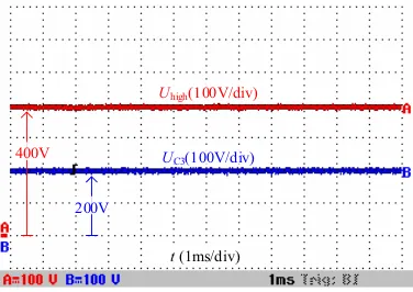
C3 can be reduced to half of the voltage Uhigh, and UC2, UC3 are
self-balanced due to the switched-capacitor technique. Similarly, the corresponding voltage equations of the proposed converter within the range of 0.5dBoost<1 can also be obtained, which are
the same as those within the range of 0<dBoost<0.5. (2) Voltage-gain in the step-down mode
As shown in Fig. 4(a) and Fig. 5(c), within the range of
dBuck<1, C1 and C3 are connected in parallel, so that the
voltages of C1 and C3 are still equal. According to Fig. 5(a)-(c)
and the voltage-second balance principle on L1 and L2, the
following equations can be obtained as
Buck C2 low Buck low
Buck C1 low Buck low
C1 C3
( )=(1 )
( )=(1 )
d U U d U
d U U d U
U U
u u
° u u
® ° ¯
(3)
Therefore, by simplifying (3), the following equations can be written as
C1 C2 C3 high
Buck
low high
2
1 2
U U U U
d
U U
°° ® ° °¯
(4)
According to (4), the voltage-gain of the proposed converter in the step-down mode is dBuck/2, which is half of the
voltage-gain of the conventional interleaved bidirectional DC-DC converter. In addition, the voltage stress of C1, C2 and
C3 are still half of the voltage Uhigh, and UC2, UC3 are still
self-balanced, which are the same as those in the step-up mode. Similarly, the voltage equations of the proposed converter within the range of dBuck<1 can also be obtained, which are
the same as those within the range of 0<dBuck<0.5. B. Inductor currents self-balance
(1)Inductor currents self-balance in the step-up mode
According to Fig. 3(a)-(c), the currents of C1, C2 and C3 are as
follows, within the duty cycle range 0<dBoost<0.5 in the step-up
mode.
'
C1 Boost s
C1
L2 Boost s s
high Boost s
C2
L1 high Boost s s
'
high C1 Boost s
C3
high Boost s s
0
0
0
I t d T
i
I d T t T
I t d T
i
I I d T t T
I I t d T
i
I d T t T
° d
° ®
d
° °¯
°
d
° °
® ® d
°
° ¯
° d
°
° ®
° d
°¯ ¯
(5)
where IL1, IL2 and Ihigh are the average currents of iL1, iL2 and ihigh,
and IC1, IC2 and IC3 are the average currents of iC1, iC2 and iC3 in
the step-up mode respectively. In addition, ' C1
I is the average current of C1 when Q2 turns on. By applying the amp-second
balance principle on capacitors C1, C2 and C3, the following
[image:5.595.52.278.223.295.2]
'
Boost s C1 Boost s L2
C1
s
' Boost
L2 C1
Boost
1 =0=
= 1
d T I d T I
i
T
d
I I
d
(6)
Boost s high Boost L1 high
C2
s
L1 high
Boost
1 =0=
1 =
1
d T I d I I
i
T
I I
d
(7)
'
Boost s high C1 Boost s high
C3
s
'
C1 high
Boost
1 =0=
1 =
d T I I d T I
i
T
I I
d
(8)
In addition, the relationship Ilow=IL1+IL2 can be drawn in the
step-up mode, according to Fig. 3. Then, substituting (8) into (6),
Ilow, IL1 and IL2 can obtained as
low high
Boost
L1 L2 high
Boost
2 1
1 1
I I
d
I I I
d
°
° ® °
°
¯
(9)
In terms of (9), IL1 and IL2 are both half of the input current
Ilow, i.e. the current self-balance is achieved in the step-up mode.
Similarly, the corresponding current equations of the proposed converter within the duty cycle range 0.5dBoost<1 can also be
obtained, which are the same as those within the duty cycle range 0<dBoost<0.5.
(2) Inductor currents self-balance in the step-down mode
The currents of C1, C2 and C3 can be written as follows within
the duty cycle range 0<dBuck<0.5, by means of Fig. 5(a), (c) and
(d), in the step-down mode.
L2 Buck s
C1 '
C1 Buck s s
high L1 Buck s
C2
high Buck s s
high Buck s
C3 '
high C1 Buck s s
0
0
0
I t d T
i
I d T t T
I I t d T
i
I d T t T
I t d T
i
I I d T t T
° d
° ®
d
° °¯
°
d
° °
® ® d
°
° ¯
° d
°
° ®
° d
°¯ ¯
-
(10)
where IL1, IL2 and Ihigh are the average currents of iL1, iL2 and ihigh,
and IC1, IC2 and IC3 are the average currents of iC1, iC2 and iC3 in
the step-down mode respectively. In addition, IC1' is the average
current of C1 when Q3 is turned off. By applying the amp-second
balance principle on capacitors C1, C2 and C3, the following
equations (11)-(13) can be obtained as
'
Buck s L2 Buck s C1
C1
s
' Buck
L2 C1
Buck
1 =0=
1 =
d T I d T I
i
T
d
I I
d
(11)
Buck s high L1 Buck high
C2
s
L1 high
Buck
1 =0=
1 =
d T I I d I
i
T
I I
d
(12)
'
Buck s high Buck s high C1
C3
s
'
C1 high
Buck
1 =0=
1 =
1
d T I d T I I
i
T
I I
d
(13)
According to Fig. 5, the current relationship Ilow=IL1+IL2 can
also be drawn in the step-down mode. Then, substituting (13) into (11), Ihigh, IL1 and IL2 can achieved as
Buck
high low
L1 L2 low
2 1 2
d
I I
I I I
°° ® ° °¯
(14)
By means of (14), IL1 and IL2 are also half of the input current
Ilow, i.e. the current self-balance is also obtained in the
step-down mode. In a similar way, the corresponding current equations of the proposed converter within the duty cycle range 0.5dBuck<1 can also be obtained, which are the same as those
within the duty cycle range 0<dBuck<0.5.
Based on the analysis previously described, inductor currents self-balance can be achieved within the full duty cycle range for the proposed converter, in both step-up and step-down modes. This contributes to accurate current sensing, and eliminates an extra control loop that may require high performance circuits to balance phase currents.
C. Voltage and current stresses of power semiconductors
(1) Voltage stress
As shown in Fig. 3(b, c) in the step-up mode and Fig. 5(b, c) in the step-down mode, power semiconductor Q1 is turned off
and Q4 is turned on, so that Q1 and C2 are connected in parallel.
Therefore the voltages of Q1 and C2 are equal. Similarly, the
voltages of the other power semiconductors can also be obtained. According to (2) in the step-up mode and (4) in the step-down mode, the voltage stress for the power semiconductors can be written as follows
high
Q1 Q4 C2
high
Q2 Q3 C1
high
Q5 C3
2 2
2
U
U U U
U
U U U
U
U U
° ° ° ® ° ° ° ¯
(15)
Based on (15), all the voltage stresses of the power semiconductors and capacitors are half of the voltage Uhigh. (2) Current stress
Q1 high
Boost
Q2 high
Boost Boost
Q3 Q4 high
Boost
Q5 high
Boost
1 1
1 1
( )
1 1 1 1
I I
d
I I
d d
I I I
d
I I
d
°
° °
°
° ® °
°
° ° °¯
(16)
Similarly, according to Fig. 5 and (14), the current stress of the power semiconductors in the step-down mode can be obtained as (17)
Q1 low
Q2 low
Buck
Q3 Q4 low
Buck
Q5 low
Buck
1 2
1
2(1 )
1 2
2(1 )
I I
I I
d
I I I
d
I I
d
° ° °
°
° ® ° ° ° °
°¯
(17)
Based on (16) and (17), it can be seen that the current stress of
Q2 is higher than that of Q1. But it is easier to choose a MOSFET
with the high rated current rather than the one with the high rated voltage. Furthermore, the proposed bidirectional converter can obtain a high voltage gain while the duty cycle is in the range of 0.5<dBoost<1 in the step-up mode or 0<dBuck<0.5
in the step-down mode. Therefore, the difference of the current stress between Q1 and Q2 is limited, and it will not affect the
selection of the power semiconductors.
D. Analysis of current ripples
(1) Analysis of current ripples in the step-up mode
In the step-up mode within the range of 0<dBoost<0.5, it is
assumed that L1=L2=L. According to Fig. 3, the current ripples
of iL1, iL2 and ilow can be derived as follows
Boost Boost s high
L1 L2
Boost Boost s high
low
(1 )
2
(1 2 )
2
d d T U
i i
L
d d T U
i
L
u u u
' ' °°
® u u u
°' °¯
(18)
Where ǻiL1, ǻiL2 and ǻilow are the current ripples of iL1, iL2 and
ilow. Similarly, the current ripples of iL1, iL2 and ilow within the
range of 0.5dBoost<1 can be described as follows
Boost Boost s high
L1 L2
Boost Boost s high
low
(1 )
2
(2 1) (1 )
2
d d T U
i i
L
d d T U
i
L
u u u
' ' °°
® u u u
°' °¯
(19)
(2) Analysis of current ripples in the step-down mode
In the step-down mode within the range of 0<dBuck<0.5, it is
also assumed that L1=L2=L. According to Fig. 5, the current
ripples of iL1, iL2 and ilow can be derived as follows
Buck Buck s high
L1 L2
Buck Buck s high
low
(1 )
2
(1 2 )
2
d d T U
i i
L
d d T U
i
L
u u u
' ' °°
® u u u
°' °¯
(20)
Where ǻiL1, ǻiL2 and ǻilow are the current ripples of iL1, iL2 and
ilow. Similarly, the current ripples of iL1, iL2 and ilow within the
range of 0.5dBuck<1 can be described as follows
Buck Buck s high
L1 L2
Buck Buck s high
low
(1 )
2
(2 1) (1 )
2
d d T U
i i
L
d d T U
i
L
u u u
' ' °°
® u u u
°' °¯
(21)
Assuming that L1=L2=L ȝ+ fs=20kHz, Uhigh=400V,
Ulow=50V~120V, and the rated output power Pn=1kW. The
current ripple rate of iL1, iL2 and ilow is shown in Fig. 8, where
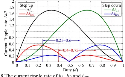
ǻi/I is defined as the current ripple rate. According to Fig. 8, the current ripple of the low-voltage side current ilow is smaller than
those of iL1 and iL2 in both step-up and step-down modes. When
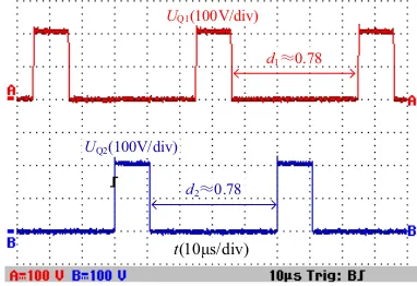
Uhigh=400V and Ulow=50V~120V, the duty cycle varies in the
range of 0.4<dBoost<0.75 in the step-up mode according to (2),
and varies in the range of 0.25<dBuck<0.6 in the step-down mode
in terms of (4). The current ripple rate of the low-voltage side current ilow is further reduced within the corresponding duty
cycle range. Taking the step-up operating state as an example, when DC source is in the range of Ulow=50V~120V, the
minimum ripple rate of the low-voltage side current is 0% when the duty cycle is dBoost ,QWKHUDQJHRIdBoost<0.5, the
maximum ripple rate of the low-voltage side current arrives at 27.4% when the duty cycle is dBoost=0.4. In addition, the
maximum current ripple rate of the low-voltage side arrives at 21.1% when the duty cycle is dBoost=0.67 within the range of
0.5<dBoost<0.75.
0 0.1 0.2 0.3 0.4 0.5 0.6 0.7 0.8 0.9 1
0 0.2 0.4 0.6 0.8 1 1.2 1.4 1.6 1.8 2
0.4~0.75
0.25~0.6 ǻiL1
ǻilow
Step up Step down
C
ur
re
n
t
R
ippl
e
ra
te
ǻ
i/
I
Duty (d)
ǻǻilow
[image:7.595.319.528.471.599.2]iL1
Fig. 8 The current ripple rate of iL1, iL2 and ilow.
E. Comparisons with other bidirectional solutions
According to the analysis above, the comparisons can be drawn among the proposed and the other bidirectional solutions in the step-up mode, as shown in Tab. 1. The bidirectional DC-DC converter in [14] only needs one inductor, but its ideal voltage-gain 1/(1-d) is limited due to the effects of parasitic resistance and extreme duty cycles. Although the voltage stress across the four semiconductors of this converter is half of the high-side voltage Uhigh, the current stress of the power
Tab. 1 Comparisons among the proposed and the other bidirectional solutions
Bidirectional
Solutions Voltage Gain
Amount of Semiconductors Amount of Inductors Maximum Voltage Stress of Semiconductors Inductor Currents Balancing
Converter in [14] Ulow/(1-d) 4 1 Uhigh/2 -
Converter in [20] Ulow/(1-d) 4 2 Uhigh YES
Converter in [25] 3Ulow/(1-d) 5 2 2Uhigh/3 When Db=2Da
Converter in [26] 2Ulow/(1-d) 4 2 Uhigh YES
Converter in [27] Ulow/(1-d)2 4 2 Uhigh+ Uhigh(1-d) When d=0.5
Proposed converter 2Ulow/(1-d) 5 2 Uhigh/2 YES
converter in [20] can reduce the current ripples in the low-voltage side, but it still has the disadvantages including the small voltage gain range and the high voltage stress across the power semiconductors. The interleaved bidirectional DC-DC converters in [25] -[27] have achieved a high voltage-gain, but the maximum voltage stress across the semiconductors of these converters are 2Uhigh/3, Uhigh and Uhigh+ Uhigh(1-d) respectively,
rather than Uhigh/2, which will increase the switching losses and
reduce the conversion efficiency. Besides, the converter in [27] can only achieve the inductor currents balance when the duty cycles are d=0.5, and the inductor currents of the converter in [25] are unbalanced when Db is not equal to 2Da. Regarding the
proposed interleaved bidirectional DC-DC converter, the number of main components is equal to that of the converter in [25] , the voltage stress across all semiconductors and capacitors is Uhigh/2, and its voltage gain is higher than that in
[14] and [20] . In addition, the inductor currents and the capacitor voltage self-balances can also be obtained within the full duty cycle range, in both step-up and step-down modes.
A. Small-signal modeling
It is assumed that the power semiconductors, the inductors, and the capacitors are all ideal. Then, the average model and the small-signal model can be obtained by using the state-space averaging method. According to Fig. 3(c)-(d) in the step-up mode (or Fig. 5(c)-(d) in the step-down mode), C1 and C3 are
connected in parallel when Q2 and Q5 turn on, and Q3 turns off.
It means the voltages across C1 and C3 are equal. So, there is an
invalid state variable. By considering the equivalent series resistance (e.g. r=0.23ȍfor C1), the coupling between the
capacitors can be removed to avoid the invalid state variables.
(1) Small-signal modeling in the step-up mode
When the proposed bidirectional converter operates in the step-up mode in the range 0<dBoost<0.5, the main power
semiconductors Q1 and Q2 have three effective switching states:
S1S2=[10, 00, 01]. ulow(t), uhigh(t), and d1(t), d2(t) are the input
variable, the output variable and the control variables respectively. iL1(t), iL2(t), uC1(t), uC2(t) and uC3(t) are the state
variables. When S1S2=10, the converter operates in Mode I (as
shown in Fig. 3(a)), and its operating time is d1(t)uTs. So, the
state space average model can be obtained as follows
L1 L2 L1 2 L2 C1 1 C1 C2 C2
2 L-Boost 2 L-Boost
C3
3 L-Boost 3 L-Boost
d ( ) 0 0 0 0 0
d 1
0 0 0 0
d ( ) ( )
d 1 ( )
0 0 0 0
d ( )
( ) d
1 1 (
d ( ) 0 0 0
d
1 1
d ( ) 0 0 0
d
i t
t
i t L i t
t i t
u t
C u t
t
u
u t
C R C R
t
u t
C R C R
t
ª º ª º
« » « » « » « » « » « » « » « » « » « » « » « » « » « » « » « » « » « » « » « » « » « »
« » «¬ »¼
« »
¬ ¼
> @> @
1
2 low
C3
T
high L1 L2 C1 C2 C3
1 1 ( ) 0 ) 0 ( ) 0
( ) 0 0 0 1 1 ( ) ( ) ( ) ( ) ( )
L
L u t
t
u t
u t i t i t u t u t u t
°
ª º °
« »
° ª º « »
° « » « » ° « » « » ° « » ° « » « » ® « » « » ° « » « »
° ¬ ¼ « »
° « »¬ ¼
° ° ° ° ¯ (22)
where RL-Boost is the equivalent load resistance in the step-up
mode. When S1S2=00, the converter is operating in Mode II (as
shown in Fig. 3(b)), and its operating time is [1-d1(t)-d2(t)]uTs.
The state space average model can be written as
L1 1 L2 L1 2 L2 C1 1 C2
2 2 L-Boost 2 L-Boost C3
3 L-Boost 3 L-Boost 1
d ( ) 0 0 0 0
d
1
d ( ) 0 0 0 0 ( )
d ( )
1
d ( )
0 0 0 0
d
d ( ) 1 1 1
0 0
d
d ( ) 1 1
0 0 0
d
i t
L t
i t i t
L
t i t
u t
u C
t
u t
t C C R C R
u t
t C R C R
ª º
ª º « »
« » « » « » « » « » « » « » « » « » « » « » « » « » « » « » « » « » « » « » « » « » « » « » « » « »
¬ ¼ «¬ »¼
> @> @
1 2 C1 low C2 C3 T
high L1 L2 C1 C2 C3
1 1 ( ) ( ) 0 ( ) 0 ( ) 0
( ) 0 0 0 1 1 ( ) ( ) ( ) ( ) ( )
L
L
t u t
u t
u t
u t i t i t u t u t u t
°
° ª º
° « » ª º ° « » « » ° « » « » ° « » « » °° « » « » ® « » « » ° « » « »
° ¬ ¼ « »
° « »¬ ¼
° ° ° ° °¯ (23)
When S1S2=01, the converter operates in Mode III (as shown in
Fig. 3(c)), and its operating time is d2(t)uTs. The state space
average model can be achieved as
L1 1 L2 L1 C1 1 1 C2
2 2 L-Boost 2 L-Boost
C3
3 3 L-Boost 3 3 L-Boost
d ( ) 1
0 0 0 0
d
d ( ) 0 0 0 0 0 ( )
d 1 1
0 0 0
d ( ) d
1 1 1
d ( ) 0 0
d
1 1 1 1
d ( ) 0 0
d
i t
t L
i t i t
t i
u t
C r C r
t u t
C C R C R
t u t
C r C R C r C R t
ª º ª º
« » « » « » « » « » « » « » « » « » « » « » « » « » « » « » « » « » « » « » « » « » « »
« » «¬ »¼
« »
¬ ¼
> @> @
1 L2 2 C1 low C2 C3 T
high L1 L2 C1 C2 C3
1
( ) 1
( ) ( ) 0 ( ) 0 ( ) 0
( ) 0 0 0 1 1 ( ) ( ) ( ) ( ) ( )
L t
L u t u t u t
u t
u t i t i t u t u t u t
°
ª º °
« »
° ª º « »
° « » « » ° « » « » ° « » ° « » « » ® « » « » ° « » « »
° ¬ ¼ « »
° « »¬ ¼
° ° ° ° ¯ (24)
Combining (22) and (23) with (24), the average model of the converter can be obtained as:
1 L1 1 2 L2 2
2 2 2
C1
1 1 1
C2 1
2 2 L-Boost 2L-Boost
C3
2 2
3 3 L-Boost 3
1 ( )
d ( ) 0 0 0 0
d
1 ( )
d ( ) 0 0 0 0
d
1 ( ) ( ) ( ) d ( )
0 0
d
d ( ) 1 ( ) 1 1 0 0
d
d ( ) ( ) 1 ( ) 1 0 0 d d t i t L t d t i t L t
d t d t d t
u t
C C r C r
t
u t d t
t C C R C R
u t d t d t
t C r C R C r
ª º « » « » « » « » « » « » « » « » « » « » « » « » « » ¬ ¼
> @> @
L1 1 L2 2 C1 low C2 C3 3L-Boost T
high L1 L2 C1 C2 C3
1 ( ) ( ) 1 ( ) ( ) 0 ( ) 0 ( ) 0
( ) 0 0 0 1 1 ( ) ( ) ( ) ( ) ( )
i t L
i t L
u t u t
u t
u t
C R
u t i t i t u t u t u t
ª º
° « »
° « » ª º
° « »ª º « »
° « » « » « » ° « »« » « » ° « » « » « » ° « » ° « »« » « » ® « »« » « » ° « »« » « »
° « »¬ ¼ « »
° « » « »¬ ¼
°
« »
°
« »
° ¬ ¼
° °¯
(25)
In the duty cycle range 0.5<dBoost<1, the main power