warwick.ac.uk/lib-publications
Original citation:
Chan, Chunwa, Mawby, P. A. and Gammon, P. M.. (2016) Analysis of linear-doped Si/SiC
power LDMOSFETs based on device simulation. IEEE Transactions on Electron Devices, 63
(6). pp. 2442-2448
Permanent WRAP URL:
http://wrap.warwick.ac.uk/79315
Copyright and reuse:
The Warwick Research Archive Portal (WRAP) makes this work of researchers of the
University of Warwick available open access under the following conditions.
This article is made available under the Creative Commons Attribution 3.0 (CC BY 3.0) license
and may be reused according to the conditions of the license. For more details see:
http://creativecommons.org/licenses/by/3.0/
A note on versions:
The version presented in WRAP is the published version, or, version of record, and may be
cited as it appears here.
Analysis of Linear-Doped Si/SiC Power
LDMOSFETs Based on Device Simulation
Chunwa Chan, Philip A. Mawby, Senior Member, IEEE, and Peter M. Gammon, Member, IEEE
Abstract— This paper presents the design and optimization
of a 600 V silicon-on-silicon carbide (Si/SiC) laterally diffused MOSFET with linear doping profile in the drift region for high-temperature applications. The proposed structure has an embedded silicon-on-insulator (SOI) layout through which the traditional graded doping theory for SOI can be applied in the Si/SiC architecture. An SOI counterpart is introduced as a benchmark and modeled alongside the proposed structure. Comparisons between them show that they have the near-identical OFF-state and breakdown characteristics, with a signif-icant tunneling leakage component emerging above 450 V. In the
ON state, the Si/SiC device has higher electrical resistance but much lower thermal resistance, leading to less self-heating and higher reliability.
Index Terms— High-temperature operation, power MOSFETs,
power semiconductor devices, self-heating, semiconductor device modeling, silicon carbide, silicon-on-insulator (SOI) technology, silicon-on-silicon carbide.
I. INTRODUCTION
C
URRENTLY, silicon-on-insulator (SOI) technology is adominant method to achieve lateral power electronics operating in high-temperature harsh environments due to fast switching speed, low leakage current, and complete electri-cal isolation [1]. However, SOI devices encounter signifi-cant self-heating effects as the buried silicon dioxide (SiO2) impedes heat transfer from the active Si layer to the substrate. Therefore, temperature is relatively high in the active layer, which increases local resistance, degrading performance and potentially stressing metal contacts or wire bonds [2]. This situation becomes more serious in power transistors, where substantial power is generated and required to be dissipated. Partial SOI (PSOI) is one solution featuring a small opening of the buried oxide (BOX) layer, typically beneath the drain [3], so that heat can escape into the substrate, thereby reducing the self-heating. Higher breakdown voltage can also be realized as potential spreads down into the substrate [3]. However, fabricating the PSOI substrate is a challenge that results in a window of limited size, as further widening of the window leads to a degradation of the insulating properties.
Manuscript received August 5, 2015; revised November 3, 2015, December 13, 2015, and January 30, 2016; accepted March 29, 2016. Date of publication April 20, 2016; date of current version May 19, 2016. This work was supported in part by the Engineering and Physical Sciences Research Council under Grant EP/N00647X/1 and in part by the Royal Academy of Engineering within the Novel interlayer cooling for harsh environment Program. The review of this paper was arranged by Editor F. Udrea.
The authors are with the School of Engineering, University of Warwick, Coventry CV4 7AL, U.K. (e-mail: [email protected]; p.a.mawby@ warwick.ac.uk; [email protected]).
Color versions of one or more of the figures in this paper are available online at http://ieeexplore.ieee.org.
Digital Object Identifier 10.1109/TED.2016.2550865
Another way of reducing self-heating effects is to use a sapphire (Al2O3) substrate as the insulating material under the Si layer, sapphire having a thermal conductivity higher than SiO2. This structure is termed silicon on sapphire (SOS) and displays better thermal and RF behavior than SOI. Signif-icant effort has been put into developing SOS, with techniques such as field plates [4], linear doping [5], super-junction [6], and radial confinement [7] having been employed to optimize design. However, compared with SOI, SOS devices are more expensive and suffer lower carrier mobility and higher trap density at the Si/Al2O3 interface [4], [8]. Recently, these issues have been improved by using a wafer bonding process that delivers 56% higher electron mobility than epitaxial methods [9]. This laid a foundation for commercializing SOS devices, but self-heating remains a problem, the thermal conductivity of sapphire being inferior to that of silicon [6].
Semi-insulating SiC offers another option to replace the BOX due to the fact that its thermal conductivity and bandgap are both about three times those of silicon, and hence well-suited for high-temperature operations [10], [11]. The imple-mentation of silicon-on-silicon carbide (Si/SiC) substrates is possible using a conventional wafer bonding or SmartCut tech-nique, as shown in [12]–[18]. Thus, the Si layer can be as good as that in SOI and relatively free of interface charge. Lateral MOSFETs have been fabricated successfully in this substrate for low-voltage applications and promising results included a significant reduction of the self-heating [17], [18]. In addition, an initial study on lateral Si/SiC diodes for high-voltage opera-tions has been carried out and shows that the self-heating effect is minimized in a thin-film Si on SiC substrate (Si/SiC), which has an ability to dissipate heat comparable to bulk SiC [19].
In this paper, we propose for the first time a linear-doped LDMOS design, using a Si/SiC substrate for minimal
self-heating effects and high-temperature applications.
Characteristics of this device are produced in 2-D simulations and compared with a similar SOI transistor. The results show that the proposed structure is more robust against self-heating at the expense of more chip area to achieve the same electrical performance of the SOI at 150 °C.
II. SIMULATEDSTRUCTURES
The first simulated structure is based upon an SOI LDMOS developed by Philips laboratories [20] that can support 660 V
and has low ON-state resistance. Leakage current is minimal
at only 1.5 nA/μm at 300 °C [20]. Therefore, it is a good
starting point to use as a benchmark for verification and comparison. Its 2-D schematic is shown in Fig. 1(a) and
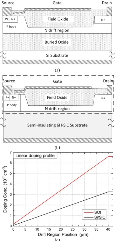
Fig. 1. Layout of the simulated (a) SOI and (b) Si/SiC LDMOS transistors, as well as (c) their doping profiles in the drift region.
established in finite-element modeling program SILVACO.
Linear doping is employed in a drift region that
is 42-μm long and 0.2-μm thick, according to [21]. The
thick-nesses of the BOX and field oxide were both 2μm. The field
oxide is covered by an extended gate contact to improve the
ON-state performance [22]. A 60-nm gate oxide is placed
on the p body region doped with 6.5×1016 cm−3, where
the channel length is 1.5 μm. It is worth noting that some
configurations may be different from those of the Philips device because not all parameters are mentioned in [20]. However, similar outcomes are found in the simulations, as demonstrated in Section IV.
As shown in Fig. 1(b), the second device is very similar to that implemented in SOI, the starting point being to implement
an identical device with a 300-μm-thick 6H-SiC substrate
modeled in place of the BOX layer. Linear doping is then similarly utilized to achieve the target voltage rating of 600 V. An inverse SOI structure (IOS) is formed comprising a gate
electrode, field oxide, and the Si layer enclosed by a box in Fig. 1(b). In this arrangement, the gate contact behaves like the substrate electrode in the SOI case as it almost entirely overlaps the field oxide and is zero-biased in the reverse blocking state [4]. Therefore, as long as the field oxide is thick enough to support the required potential, this IOS layout is equivalent to ordinary SOI. This idea originates in [4], where a step field oxide is used for a uniform-doped SOS device. This design was then refined using linear doping to increase the breakdown voltage to 600 V, with reduced resistance [5]. This concept is applied in the proposed Si/SiC structure and the calculated concentration profile in the drift region for 600 V is presented in Fig. 1(c), along with that of the SOI counterpart. The profile for the SOI is much steeper and the maximum doping is two times higher. The reason for this is that a dual-plate structure is present in SOI that generates a symmetrical charge modulation in the Si layer [22].
III. SIMULATIONSETUP
Simulations of the two structures in Fig. 1 have been carried out using SILVACO. The substrate electrode is grounded and defined as a thermal contact for electrothermal simulations. Thermal conductivities of materials are set to be power func-tions of temperature. No fixed charges are configured along the Si/SiO2and Si/SiC interface. Carrier lifetimes are not constant and decreased with increased impurity concentration. Indirect band-to-band tunneling model is chosen and activated in the top Si layer.
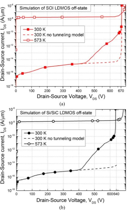
In theOFF-state, isothermal simulations (those ignoring the effects of self-heating) at 27 °C and 300 °C are used given that the reverse current is not enough to heat the devices. The impact of tunneling and avalanche mechanisms on leakage current and breakdown is investigated by simulating the struc-tures with and without the tunneling mechanism activated, as shown in Fig. 2.
In the ON-state, the dc characteristics of the devices are analyzed using a gate voltage ranging from 3 to 20 V. Both isothermal and nonisothermal models are used to compare and assess the self-heating effects in the structures. The ambient temperature is 27 °C in these simulations.
Next, the switching characteristics of the devices are sim-ulated via an inductive switching setup. The gate is switched
at 200 kHz via a pulse signal, through a 10- gate resistor,
with a 50% duty cycle. The peak voltage is 10 V and the time for rising and falling is equal to 1 ns. The drain contact is linked to a parallel network composed of a diode and an inductor. Attached to this network is a current-limiting resistor connected to a 360 V voltage source. For this simulation, the channel widths of the SOI and Si/SiC are 1 and 1.65 cm, respectively, which leads to the same electrical resistance and current, at the initial temperature of 150 °C. The SOI or Si/SiC transistor is modeled in this circuit for two cases, one
of which has a 2-mH inductor and 1800- current-limiting
Fig. 2. OFF-state I –V characteristics of (a) SOI and (b) Si/SiC LDMOS.
IV. SIMULATIONRESULTS
The proposed Si/SiC LDMOSFET transistors are first
benchmarked to the SOI devices using their OFF-state
characteristics. Isothermal and nonisothermal simulations of ON-state performance are then carried out to show the ability of these devices to handle the effects of self-heating.
A. OFF-State Performance
Generally speaking, the total leakage current can be char-acterized as the sum of the diffusion component in the neutral region and the generation current in the depletion region [23]. In [24], a large tunneling current is reported in a thin-film SOI structure at room temperature, so this is taken into
account in the model. Fig. 2(a) and (b) shows the OFF-state
[image:4.612.339.536.58.514.2]behavior for the SOI and the Si/SiC, respectively. The diffusion current is insignificant in these two structures as the linear doping profile permits full depletion of the thin film. At room temperature, both devices can support more than 600 V and their leakage currents are in the range 10−17 to 10−14 A/μm below 450 V. Beyond this voltage, the tunneling component becomes dominant, raising the total leakage current in both cases. This reveals that both structures have a depletion zone in the drift region, with field strength high enough to allow band-to-band tunneling. This occurs due to the highly doped Si film and inherent SOI layout that induces vertical depletion, causing a strong electric field in the space charge region.
Fig. 3. Isothermal modeling of (a) SOI and (b) Si/SiC LDMOSON-state characteristics and (c) their ohmic regions.
At 300 °C, the breakdown voltage increases in both structures to 680 V, a result indicative of an avalanche break-down mechanism rather than tunneling [23]. However, this relation is not as strong as that of a 1-D junction shown in [23], meaning that the uniform electric field in the drift region compensates for some of the energy of travelling carriers lost at high temperature, thereby reducing the increment of the breakdown voltage. At 300 °C, the leakage current is
also increased to around 10−8 A/μm. The contribution at
Fig. 4. Effect of self-heating on forward characteristics of (a) SOI and (b) Si/SiC LDMOS, as well as (c) their junction temperature.
condition and the contribution of the tunneling component can be disregarded [24].
B. ON-State Performance
1) Isothermal Simulation and the Effects of Removing the BOX: Fig. 3 demonstrates the ON-state behavior of the two structures at 27 °C using an isothermal model that ignores the effects of self-heating. Common to both transistors are threshold voltages of 2 V (not shown) due to the identical configuration of the channel regions. Furthermore, neither device suffers a significant reduction in breakdown voltage at high gate bias because both designs have a high impurity dose at the drain-end of the drift region, thus reducing the kirk effect [1] and enlarging the electrical safe operating area. It is also noted that there is no kink effect [25] in the saturation regime of the devices. The common reason for this [25] is
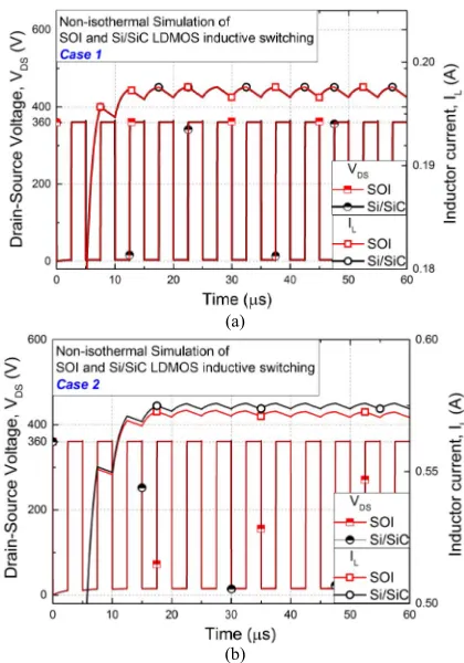
Fig. 5. Drain–source voltage and inductor current for the two transistors during VGS = 10 V, 200 kHz switching nonisothermal simulations. The
inductor and current-limiting resistor are 2 mH and 1800 in (a) Case 1 and 1 mH and 600in (b) Case 2.
that the grounded p body is used and allows for extraction of excess holes generated via ionization process.
In the ohmic region, the SOI device conducts more current due to its doping being two times higher than the Si/SiC equivalent [see Fig. 3(c)]. However, this configuration does not double the SOI current in the saturation region. Instead, both cases have a similar current level at large drain biases up to 100 V, meaning that a counter effect exists in the SOI and is enhanced with increasing drain voltage. Given that the same channel and geometry of the drift region are designed in the two devices, this phenomenon is likely caused by the BOX layer. At relatively high drain bias, the SOI drift region is depleted from above by the gate field plate and below by the charge-rich region under the BOX. These effectively squeeze the drift region from both sides, limiting carrier transport to the middle undepleted region. In the Si/SiC case, the removal of the BOX removes the bottom field plate effect, leaving the bottom of the drift region undepleted. Therefore, the SOI resistance increases faster against drain voltage and eventually reaches a value comparable to that of the Si/SiC.
2) Nonisothermal Simulation and the Effects of Self-Heating: The effects of self-heating in both the SOI and Si/SiC
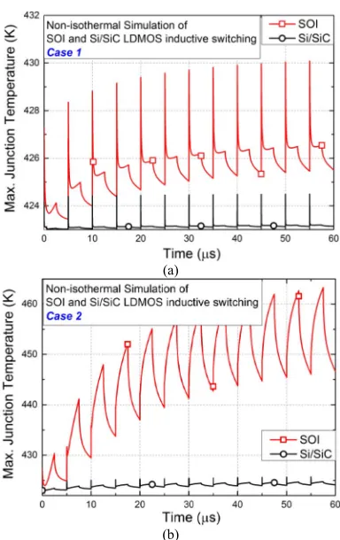
[image:5.612.83.267.57.510.2]Fig. 6. Dynamic temperature response of the two transistors in the nonisothermal switching for (a) Case 1 and (b) Case 2.
well as in the saturation regime at low gate bias (e.g., 3.5 V). However, they diverge as resistance and current increase. This gives rise to substantial power losses that increase the local temperature, thereby reducing carrier mobility. This situation is worsened at increasing gate and drain voltages and even-tually significant deviation occurs, with the effect of negative resistance becoming evident in the nonisothermal cases. In the Si/SiC device, this is not obvious until the gate voltage is raised to 5 V as opposed to around 4 V in the SOI. Fig. 4(c) is from the same simulation and shows the corresponding temperature rise for each nonisothermal I –V simulation. Internal temperate rises sharply against drain voltage in the SOI, with the temperature at any given point over four times greater in this substrate than in the Si/SiC. Furthermore, temperature sensitivity to gate voltage is lower in the Si/SiC, which reduces the risk of thermal-induced failures at high gate biases.
Fig. 5 shows the drain–source voltage and inductor current for each LDMOSFET under the inductive switching conditions described, in detail, in Section III. Two cases are considered in which the transistors are simulated under high-and low-current conditions, both within the linear region. It can be seen that the two LDMOSFETs have the same performance under low current conditions (Case 1). Under high-current conditions (Case 2), a small current mismatch exists due to increased self-heating effects.
[image:6.612.355.517.59.387.2]Fig. 6 shows the differing self-heating effects, presenting the corresponding junction temperature of the transistors for both conditions. In both cases, the SOI heats up faster and
Fig. 7. Temperature contour of (a) SOI and (b) Si/SiC under VDS=15 V, VGS=10 V conditions (axes units:μm).
reaches a higher steady-state temperature. The pulsed opera-tion allows a period when the devices can be cooled down but introduces transient losses that can be substantial at high frequency. In Case 1, temperature spikes appear as the SOI
or Si/SiC device is turned ON, meaning that high power is
dissipated in this dynamic state. However, these peaks are only very short in duration and the temperature drops briefly,
before ON-state losses dominate. After this, the conduction
current raises the temperature for as long as the transistor
is ON. In Case 2, the device delivers a current about three
times that of Case 1, which accounts for the rapid temperature response in the SOI [see Fig. 6(b)]. The temperature spikes
due to turn-ON losses are hardly seen in this waveform and
the majority of heating is due to the conduction losses. If this pulse action continues, the temperature will rise and eventually fluctuate around a steady-state value. The increase in temperature leads to a degradation in the device’s electrical and thermal properties, causing an increase in losses compared to those at the initial temperature.
in the SOI, thereby increasing reliability. The drawback is that this layout requires 65% more chip area than the SOI at 423 K but smaller external heat sinks can be employed due to this thermally aware design, which can lower the total volume of the power module.
In Fig. 7, temperature distributions for the SOI and Si/SiC transistors can be seen with the gate and drain contact supplied by 10 and 15 V dc voltage source, respectively. This bias condition is similar to those voltages across the
LDMOSFET’s terminals during the ON-state of Case 2 for
inductive switching. With the ambient at 423 K, the maximum temperature in the Si/SiC is 436 K, compared to 502 K in the SOI. These temperatures exceed those in Fig. 6, due to being under dc conditions. Both devices have a hot spot located at the source side of the drift region, from which heat spreads toward other areas, forming a nonuniform temperature profile. However, thermal diffusion is hampered in the SOI due to the BOX, which elevates the temperature in the left part of the device and threatens the gate and source contact. In the Si/SiC transistor, the SiC substrate removes most of the heat from the Si, which reduces the temperature gradient in the drift region. As a result, the Si/SiC transistor can be operated with a higher power for a given junction temperature, at the same power for a much reduced junction temperature, or at a similar power level at an elevated ambient temperature.
V. CONCLUSION
A new Si/SiC power device is introduced with improved thermal management ability than an equivalent device imple-mented in SOI. Simulations of a lateral power MOSFET were implemented and individually optimized in SOI and Si/SiC substrates. The SOI device, which was based on a Philip’s LDMOS transistor [20], was used as the benchmark for the Si/SiC device, the BOX layer having been removed and replaced with a semi-insulating 6H-SiC substrate, forming an inverted SOI architecture.OFF-state characteristics, leakage current and breakdown voltage, are similar in both devices. The leakage current, at high drain bias (>450 V), is dominated by tunneling at low temperature, but by generation at 300 °C. Blocking voltages increase with rising temperature, meaning that the breakdown is determined by an avalanche process. In spite of higher electrical resistance, less power is converted into temperature due to lower thermal resistance provided by the SiC substrate, as can be observed in dc and inductive switching simulations. In addition, a lower peak junction tem-perature is achieved in the Si/SiC structure with a temtem-perature distribution more uniform in the drift region. It can be con-cluded that LDMOSFETs implemented in the Si/SiC substrate have the potential to be operated more reliably in traditional applications (25 °C to 175 °C), with the potential to operate in the high-temperature harsh environment up to 300 °C.
REFERENCES
[1] A. Nakagawa, “Power IC technologies,” in The VLSI Handbook, 2nd ed. Boca Raton, FL, USA: CRC Press, 2007.
[2] Y.-K. Leung, Y. Suzuki, K. E. Goodson, and S. S. Wong, “Self-heating effect in lateral DMOS on SOI,” in Proc. ISPSD, May 1995, pp. 136–140.
[3] H. T. Lim, F. Udrea, D. M. Garner, and W. I. Milne, “Modelling of self-heating effect in thin SOI and partial SOI LDMOS power devices,” Solid-State Electron., vol. 43, no. 7, pp. 1267–1280, Jul. 1999.
[4] J. Roig, D. Flores, J. Rebollo, S. Hidalgo, and J. Millan, “A 200 V silicon-on-sapphire LDMOS structure with a step oxide extended field plate,” Solid-State Electron., vol. 48, no. 2, pp. 245–252, Feb. 2004.
[5] J. Roig, D. Flores, I. Cortes, S. Hidalgo, and J. Millan, “Thin film SOI and SOS LDMOS structures with linear doping profile and enlarged field plate,” in Proc. 24th Int. Conf. Microelectron., vol. 1. May 2004, pp. 141–144.
[6] S. G. Nassif-Khalil and C. A. T. Salama, “Super-junction LDMOST on a silicon-on-sapphire substrate,” IEEE Trans. Electron Devices, vol. 50, no. 5, pp. 1385–1391, May 2003.
[7] S. Krishnan et al., “The radial confinement: A new approach to high voltage lateral power devices,” in Proc. Int. Semiconductor Conf. (CAS), vol. 1. Oct. 2000, pp. 349–352.
[8] T. Erlbacher, “Lateral power transistors with charge compensation pat-terns,” in Lateral Power Transistors in Integrated Circuits. Switzerland: Springer, 2014, pp. 105–131, ch. 6.
[9] G. P. Imthurn, A. M. Miscione, K. Landry, A. Vaufredaz, T. Barge, and C. Lagahe-Blanchard, “Strain reduction in silicon-on-sapphire by wafer bonding,” in Proc. IEEE Int. SOI Conf. (SOI), Oct. 2011, pp. 1–2. [10] P. G. Neudeck, R. S. Okojie, and L.-Y. Chen, “High-temperature
electronics—A role for wide bandgap semiconductors?” Proc. IEEE, vol. 90, no. 6, pp. 1065–1076, Jun. 2002.
[11] P. M. Gammon, “Silicon and the wide bandgap semiconductors, shaping the future power electronic device market,” in Proc. ULIS Conf., Warwick, U.K., Mar. 2013, pp. 9–13.
[12] F. Udrea, A. Mihaila, and R. Azar, “Silicon/oxide/silicon car-bide (SiOSiC)—A new approach to high-voltage, high-frequency inte-grated circuits,” Mater. Sci. Forum, vols. 389–393, pp. 1255–1258, Apr. 2002.
[13] S. G. Whipple, J. T. Torvik, R. E. Treece, and J. T. Bernacki, “Demonstration of hybrid silicon-on-silicon carbide wafers and electrical test structures with improved thermal performance,” Mater. Res. Soc., vol. 911, May 2006.
[14] P. M. Gammon et al., “Integration of on Si/SiC heterojunctions for the gate architecture of SiC power devices,” Appl. Phys. Lett., vol. 97, no. 1, p. 013506, Jul. 2010.
[15] M. R. Jennings et al., “Si/SiC heterojunctions fabricated by direct wafer bonding,” Electrochem. Solid-State Lett., vol. 11, no. 11, pp. H306–H308, Sep. 2008.
[16] A. Pérez-Tomás et al., “Si/SiC bonded wafer: A route to carbon free SiO2 on SiC,” Appl. Phys. Lett., vol. 94, no. 10, p. 103510,
Mar. 2009.
[17] H. Shinohara, H. Kinoshita, and M. Yoshimoto, “Si metal-oxide-semiconductor field-effect transistor on Si-on-SiC directly bonded wafers with high thermal conductance,” Appl. Phys. Lett., vol. 93, no. 12, p. 122110, Sep. 2008.
[18] S. Lotfi, L.-G. Li, Ö. Vallin, L. Vestling, H. Norström, and J. Olsson, “LDMOS-transistors on semi-insulating silicon-on-polycrystalline-silicon carbide substrates for improved RF and thermal properties,” Solid-State Electron., vol. 70, pp. 14–19, Apr. 2012. [19] C. W. Chan et al., “Simulations of a lateral PiN diode on Si/SiC substrate
for high temperature applications,” Mater. Sci. Forum, vols. 821–823, pp. 624–627, Jun. 2015.
[20] E. Arnold, T. Letavic, S. Merchant, and H. Bhimnathwala, “High-temperature performance of SOI and bulk-silicon RESURF LDMOS transistors,” in Proc. ISPSD, May 1996, pp. 93–96.
[21] S. Merchant, E. Arnold, H. Baumgart, S. Mukherjee, H. Pein, and R. Pinker, “Realization of high breakdown voltage (>700 V) in thin SOI devices,” in Proc. ISPSD, Apr. 1991, pp. 31–35.
[22] T. Letavic et al., “High performance 600 V smart power technology based on thin layer silicon-on-insulator,” in Proc. ISPSD, May 1997, pp. 49–52.
[23] S. M. Sze and K. K. Ng, “p-n junctions,” in Physics of Semiconductor Devices, 3rd ed. New York, NY, USA: Wiley, 2007, pp. 97, 103–104, and 113.
[24] S. Merchant, E. Arnold, and M. Simpson, “Tunneling in thin SOI high voltage devices,” in Proc. ISPSD, May 1995, pp. 130–135.
Chunwa Chan was born in Guangdong, China, in 1989. He received the M.Sc. (Hons.) degree in electronic systems from the University of Warwick, Coventry, U.K., in 2013, where he is currently pursuing the Ph.D. degree in power electronics.
His current research interests include develop-ing high temperature power devices usdevelop-ing Si/SiC substrates, and other SOI family members, namely Si/SiO2, Si/Al2O3, and silicon on nothing.
Philip A. Mawby (S’85–M’86–SM’01) received the B.Sc. and Ph.D. degrees in electronic and electrical engineering from the University of Leeds, Leeds, U.K., in 1983 and 1987, respectively.
He joined the University of Warwick, Coventry, U.K., in 2005, as the Chair of Power Electronics. He has authored or co-authored over 100 journal and conference papers.
Peter M. Gammon (S’09–M’11) received the M.Eng. and Ph.D. degrees in electronic and electrical engineering from the University of Warwick, Coventry, U.K., in 2006 and 2011, respectively.