Abstract: The field of digital electronics has been directly towards to the low power digital system. The use of very large scale integration technology in high performance computing, wireless communication, consumer electronics has been rising at a very fast rate. The challenge for VLSI technology is growing in leakage power consumption. Wide utilizations of memory storage systems in modern electronics triggers a demand for high performance and low area implementation of basic memory component and one of the most state holding element is D Flip Flop. In this paper analysis of power and delay is done for D flip flop using different technologies like C2MOS, POWER PC, TSPC, SAER DFF,etc
Keyword s: D flip-flop; propagation delay; C2MOS,TSPC,POWERPC etc.
I. INTRODUCTION
In the past, the major concerns of VLSI designers were area,cost, performance and reliability. Low power dissipation
became a highly design concern and become more important as we move to all mobile computing and communications. The latest advancement in computing technology has set up a goal for high performance with low power consumption for vlsi designers. Flip-flops or the data storage elements are almost an essential component of every sequential circuitry. Among various Flip-flops, D flip-flop is commonly used. It captures the value of the D input at a particular predefined portion of the clock pulse (rising or falling edge of the clock) and its output is not affected at other parts of the clock. From the timing perspective, delay produced by flip-flops consumes a large part of the cycle time while the operating frequency increases. Over the past 4 decades CMOS technology have gone under drastic scaling with the view of integration ,density, high speed and low power dissipation.. Flip flops are important state holding and timing elements in digital circuits. The performance of D flip flop is much important to conclude the performance of the whole circuit. With increasing use of mobile devices, consumer electronics market demands a stringent constraint on reducing power consumption. Designers are striving for small area, low power and higher speed due to increasing demand of portable devices.. The need for comparing different design is the main motive of this paper.
II. D FLIP-FLOP TOPOLOGIES
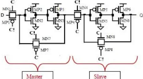
A. Transmission gate (TG) based D flip-flop
Fig. 1 shows the D flip-flop designed using four CMO transmission gates and four inverters. First stage is the master stage which is positive level sensitive and the second stage is
the slave stage which is negative level sensitive. During the positive clock pulse master follows the input while slave stores the previous input at the output (Q). When clock (C) changes from ‘1’ to ‘0’ or inverted clock (C!) from ‘0’ to ‘1’,slave becomes transparent and allows the previous input to
pass through to the output, and at that time there is no effect of input on master as it is opaque.
B. True single phase clock (TSPC) D flip-flop
Fig. 1. Sixteen-transistor (16T) transmission gate (TG) based static D flipflop
Fig. 2. Eleven-transistor (11T) true single phase clock (TSPC) dynamic D flip-flop.
[image:2.612.199.427.95.221.2]C. Clocked CMOS D Flip-Flop
Fig. 3 shows the clocked CMOS D flip-flop. In this circuit also clock and inverted clock are used. It also consists of master and slave stages. Master follows the D-input when clock (C) = ‘1’. At that time slave is opaque but its regenerative feedback loop is transparent therefore the output at Q is stable. When clock= ‘0’ master is opaque but its regenerative feedback loop is transparent therefore storing the previous D-input. This time slave is on and this D-input stored by the master is reflected at the output and is maintained till another falling edge is encountered.
Fig. 3. Twenty-transistors (20T) clocked CMOS D flip-flop.
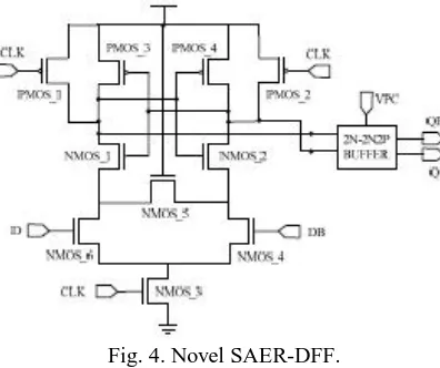
D. Novel Sense Amplifier Energy Recovery flip-flop (SAER)
Fig. 4. Novel SAER-DFF.
E. Push-Pull D Flip-Flop
[image:3.612.198.424.419.547.2]In Fig. 6 one extra TG and an inverter are added between the outputs of master and slave latches to get push-pull effect at the slave latch. This helps the input and output of the output inverter to be driven to the opposite logic values during switching. This additional path adds four extra MOSFETs but reduces the “clock to output” delay from two gates in conventional D flip-flops to one gate. To compensate for that increase in the number of MOSFETs, two TGs are removed from the feedback paths as it was in the case of Fig. 1. This circuit is comparatively faster than the rest.
Fig. 5. Sixteen-transistors (16T) push-pull D flip-flop.
F. Data Transition Look-Ahead D Flip Flop
Figure.6, shows the proposed data transition look ahead D flip flop. The transmission gates TG4 and TG5 (DL) do the data transition look ahead. It compares the hold data at the output with the respective input data and enables the flip flop to write the data, accordingly. The DL block act as an XNOR gate. For example, when D = Q = 1, the clock is inactive and transmission of data is not required. But, when D = 1, Q = 0, the clock is enabled and data gets transmitted. Clock control block consists of the transmission gate TG6 followed by an NMOS transistor. The clock control signal [2] depends on the DL’s output. The input to the clock control is given by the external clock CSP and divides into CK and CKN. DLDFF is triggered by the positive edge of the clock. When an input data D is the same as the hold data Q, the DL circuit makes P1 low. This turns the transmission gate in the clock control circuit off. As a result, CK and CKN do not transmit. CK and CKN transmit only when D and Q are different. When D
Fig.6. Data Transition Look-Ahead D Flip Flop
G. Power PC
[image:4.612.179.433.276.411.2]The main advantage of POWER PC D flip flop is short circuit path and low power feedback.The circuit diagram of D Flip flop using POWER PC is shown in figure 7.
Fig. 7. Power PC based DFF
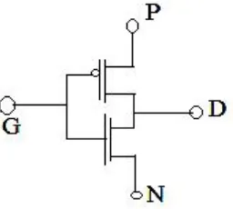
H. 6 Transistor D-Flip-Flop based on GDI Technique
The GDI technique is of more important because it uses only couple of transistors to construct a design. As the operation involves only two transistors, it could show better results in terms of Power Dissipation, Speed as well as the area occupied. This technique is most predominant for designing circuits in MOSFET technology. A basic GDI cell contains four terminals – G node (the common gate input of the n MOS (Negative channel Metal-Oxide Semiconductor) and p MOS (Positive channel Metal-Oxide Semiconductor) transistors), P node (the outer diffusion node of the p MOS transistor), N node (the outer diffusion node of the n MOS transistor), D node (the common diffusion of both transistors). P, N and D may be used as either input or output nodes, depending on the circuit structure shown in Fig.7. Multiple-input gates can be implemented by combining several GDI cells .GDI enables simpler gates, lower transistor count, and lower power consumption in many implementations. This technique allows reducing power consumption, propagation delay, and area of digital circuits while maintaining low complexity of logic design. The overall area and complexity of the circuit is minimized using GDI technique. Most of the functions which are complex (6-12 transistors) in CMOS, are very simple (only 2 transistors per function) in GDI design method.
[image:4.612.241.369.594.709.2]Fig. 8. 6 transistor D-Flip-Flop using GDI technique
III. RESULTS AND DISCUSSION
D-ff type POWER
DISSIPATION (μW)
Propagation delay (ns)
Transmission gate (TG) based D flip-flop
.48 19
True single phase clock (TSPC) D flip flop
.53 .29
Clocked CMOS D Flip-Flop .52 4.17
Novel Sense amplifier energy recovery flip-flop (SAER)
.572 34.81
Push-Pull D Flip-Flop 2.48 8.5
Data Transition Look-Ahead D Flip Flop
.684 1.107
Power PC .09 30
DFF based on GDI 2.43 2.78
IV. CONCLUSION
This work analyses and compares various known and less known D flip-flop circuits. The considered circuits can be employed for designing other complex memory and sequential
circuits. It is concluded from power dissipation comparison that power pc has lowest power dissipation and in propagation delay comparison TSPC has least propagation delay . So it is better to use TSPC logic style to design a system where fast speed is required and power PC flip flops for power conservative circuits.
REFERENCES
[1] Performance Evaluation of 6 Transistor D-Flip Flop based Shift Registers using GDI Technique International Journal of Advanced Research in Computer
and Communication Engineering Vol. 3, Issue 3, March 2014.
[2] Cooke.M, Mahmoodi- Meimand .H, Roy.K, "Energy recovery clocking scheme and flip-flops for ultra low-energy applications," Low Power Electronics and
Design. Proceedings of then International Symposium on ISLPED '03, Pp. 54-59, 2003.
[3] .S. Borkar, “Designing reliable systems from unreliable components: the challenges of transistor variability and degradation,” IEEE Micro, vol. 25, no. 6, pp.
10–16, Nov. Dec. 2005
[4] A. Islam, A. Imran and M. Hasan, “Robust Subthreshold Full Adder Design Technique,” IEEE International Conference on Multimedia, Signal Processing and
Communication Technologies (IMPACT), AMU, Aligarh, India, Dec. 17-19,2011. pp. 99 – 102.
[5] Ahmed Sayed and Hussain Al-Asaad." A New low power highperformance flip-flop", IEEE International Midwest Symposium.