Abstract—This paper contains a new series single phase active power filter based on high input power factor and low input harmonics, it is for electrical power quality purposes. We developed it in order to define new control schemes characterized by simple control algorithms and a reduced number of current transducers. The filter is designed to meet the requirements of voltage-sourced harmonic loads it is based on a load current estimation using a DC capacitor voltage of active power filter sensing the load current. The proposed filter can improve the problems of conventional small and medium non-linear loads like as computers, system of computers, washing machines, faxes, photocopier machines printers…etc and it also can suppress the harmonic current and compensate for the reactive power at the float charge mode. In general, this paper deals with a non-linear loads like as a house loads. The experimental results verify that the proposed filter has the expected performance [1][2].
Index Terms—Series active power filter (SAPF), non linear loads, power system harmonics
1
I. INTRODUCTION
The power conversion using the thyristor rectifier and all electronic devices or computers machines will result in the problems of poor input power factor and high input harmonic current and hence causes much distorted voltage. If the mains voltage is undistorted, but non-linear loads are connected to the electrical grid, the current harmonics produced will cause voltage distortions at the load terminals, hence, the loads absorb distorted currents causing heat lost exceeds in most cases 35% of the consumed power [3].
The experimental measurement, of both, load current iL
and load voltage (VL) are done, before and after correction,
to ensure that the relative large phase difference, between
the main voltage (Vs) and the line currents, becomes very
small and the power factor (PF) becomes approximately one (PF=1), as well as the shape of the current becomes clearly sinusoidal and in-phase with the main-voltage, after adding
an additional voltage (Vf) extracted from the proposed filter.
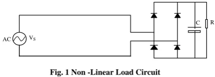
Where the resistance R and the capacitance C with the four diodes are represent the non linear Load [4].
The proposed prototypes filter achieving both tasks by using digital signal processor (pic16f877). The main target here is to compensate for voltage sag and voltage unbalance very effectively. Fig. (1) illustrates the distorted system that
is formed of a non-linear load; the load is formed of 40
μ
fcapacitor in parallel with 33Ω resistor, across a diode
Manuscript received May 15, 2009. The author is with the Hariri Canadian University Almechref - Aldamour – Lebanon (phone: 961-5-601386) e-mail: [email protected]
bridge. This non-linear load is approximately similar to a load formed of 2 or 3 personal computers.
A passive filter can be used to compensate the mentioned problems, but it is very limited, namely: they only filter the
frequencies for which they have been previously tuned, its operation cannot be limited to a certain load, resonances can occur.
II. CONTROL ALGORITHM AND THE GENERAL DESCRIPTION OF THE CONTROL
THEORY
Active power filter (APF) has been proposed since 1970s. An APF is configured from switching converters or better known as inverters that are based on pulsed operation and can be categorized as a nonlinear dynamic system [5].
A. Connection and operating mode
Fig. (2) shows the connection of the SAPF and the main components of the proposed system, the SAPF, the adjustable controller, current sensor, current limiter, nonlinear load and a power resistor R used to show the instantaneous current of the load before and after corrections
New Series Active Power Filter for Computers
Loads and Small Non-Linear Loads
Mohamed Tarnini
AC VS
D1
T1
D2
T2
D4
T4
D3
T3
C di/dt Limeter
L
C R
Non linear load
DIGITAL CONTROLLER AND FIRING CIRCUIT
R=1ohm
uR = i (oscilloscope)
VS (Oscilloscope)
Current sensor EARTH
AC VS
[image:1.595.329.542.263.339.2]C R
[image:1.595.316.552.589.741.2]Fig. 1 Non -Linear Load Circuit
T1
T3
+ -
i
i +
C T2
T4
- +
+ C i
i
-i +
i
D2
D4
+ D1
D3 i
+ -+
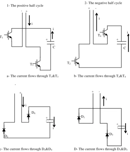
i a- The current flows through T1&T3 b- The current flows through T2&T4
c- The current flows through D2&D4 D- The current flows through D1&D3
1- The positive half cycle 2- The negative half cycle
Fig. (3) displays the switching operating principle of the filter [6] and Fig. (4) displays the circuit operating modes. It can be shown that in the positive half cycle, the operating
transistors are (T1&T3), the operating diodes are (D2&D4)
while during the negative half cycle the operating transistors
are (T2&T4), and the operating diodes are (D1&D3). At a
fixed time interval, the line current is measured and checked. When the line current below the reference current, the appropriate pair of transistors are turned on and hence, the capacitor C is connected to the line circuit, in such a way, to increase the value of the load current above the value of the reference current and thus discharging the capacitor [12][13]. When the actual current is above the reference current all transistors are turned off, and the inductance circuit will force the current to flow through the appropriate pair of free wheeling diodes and hence, the capacitor C is connected in such away that its voltage brings about the drop of the
current below the reference value which means that the capacitor is charged.
In Fig. (2) if the load DC voltage is assumed constant
(Udc), the input voltage of the load (VL) will be square wave,
such that:
⎩ ⎨ ⎧ − =
current line the of cycle half negative the in U
current line the of cycle half positive the in U V
dc dc
L (1)
B. Formulas
Assuming that the filter voltage compensates for the load harmonic voltage, we can consider only the behavior of the fundamental current and voltage.
) t sin( V
Vs= m ω
(2)
) t sin( dc U 4 L
V ω
π
= (3)
) t sin( I
i= m ω (4)
L f
s v
dt di L v
v = + + (5)
) t cos( I L ) t sin( ) U 4 V (
vf = m−π dc ω − ω m ω
(6)
At steady state case the capacitor will neither receive or
deliver energy or power (PC=0)
dt ) t sin( I v P
T m f C =∫
0
ω
0
0
2 =
∫ − −
= (I (V 4U )sin( t) L I cos(t)sin( t))dt
T
2 m dc
m
m π ω ω ω ω (7)
Moreover, this gives,
dc
m U
4 V
π
= (8)
Equation (8) gives the relation between the maximum of the source voltage and the required DC voltage of the load, in order to have constant voltage on the filter capacitor at steady state when operates in unity power factor mode.
III. EXPERIMENTAL SETUP
The main goal of the series active power filter is to eliminate the voltage harmonics. In this case, the reference voltage is always known and it is installed in a pic16f877 as 80points (point by point of known reference voltage and of known fundamental value) the time difference between two
consecutive points isΔt=250μs. Then, it is possible to
generate the reference synchronized with the main voltage and thus we can use the controller algorithm. Also it can be noted that the active filter performance is dependent on the time responses of the AC current and DC voltage control loops. However, the dynamic behavior of the filter is mainly affected by the time response of the AC current loop that must be designed in order to track the reference current waveforms closely
The reference current is obtained by extracting the fundamental from the nonlinear load current off-line. Then the reference current is discretized into HEX into samples
with sampling period Δt=250μstaking into consideration
the scaling of the Hall Effect sensor and the signal conditioning circuits.
t
tp
T1, T3
T2, T4
i-actu al
i-refe ren ce
D2, D4
i
[image:2.595.51.243.56.224.2]0
Fig. 3 Operating Principle of the Proposed Filter
Fig. 4 Circuit Operating Mode (a) Current Throught T1 and T2 in the Positive Half Cycle (b) Current through T3 and T4 in the
Negative Half Cycle (c) Current Through D1 and D2 in the
Positive Half Cycle (d) Current through D3 and D4 in the
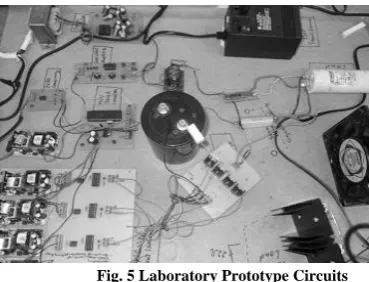
[image:2.595.51.274.257.516.2]Fig. 5 Laboratory Prototype Circuits
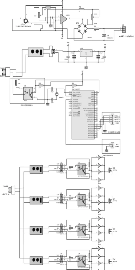
We built and tested a laboratory prototype of the single-phase active power filter, of Fig. (5), with the same power circuit parameters specified in table 1. The complete control circuit describes clearly, and the controller used is PIC16F877 microcontroller. In the following, a complete and detailed description for each part of the control circuit as well as the software program procedures is described. The simple control circuit consists of five parts
1- Power supply and zero crossing detector 2- Hall-effect current sensor and signal
conditioning circuit.
3- Microcontroller circuit
4- Driving circuit for MOSFETs
5- The inverter bridge
For more details, see Fig. (11)
C. Zero-Voltage-Crossing Detector Circuit
It is used to inform the microcontroller in which half cycle the supply voltage is at any instant. Output is then limited by 5v before being applied to the external interrupt of the microcontroller. By software, when enabling the rising edge external interrupt or the falling edge external interrupt, the microcontroller can detect the positive half cycle or the negative half cycle of the supply voltage, respectively.
D. Hall-Effect Current Sensor and Signal
Conditioning Circuit
The Hall-effect sensor used is RS-286-333 in order to
obtain voltage output; pin 1 and 4 must be linked. The sensor is rated 50A and its output at full load is 5V (i.e 100mV / 1A) and it has a larger bandwidth (up to 100 KHz)
and fast response time (<1
μ
s)The instantaneous voltage output must be amplified before being applied to the microcontroller and then added with a small DC negative voltage to neutralize the small drift (positive DC bias) associated with the instantaneous output voltage. A LM324 OP-AMP is used to perform both tasks. Finally the output must be full wave rectified because the microcontroller does not accept negative voltage and also the output must be limited by a 5V zener-diod
E. Microcontroller
The microcontroller used in this paper is PIC (16f877). The instantaneous output voltage of the Hall Effect and signal conditioning circuit is applied to the first analog input, of the analog to digital module; also the output of the zero crossing detector circuit is applied to the external interrupt of the microcontroller. According to the inputs, and based on the assemble program, installed in the PIC, the controller give the order to a specific MOSFETs through the driving
circuit to work. The software is assembled using MPLAP and the generated HEX file is downloaded through any downloader deals with PIC microcontroller.
F. Driving Circuit
The 4 output gating of the microcontroller is applied to a 4 optocoupler units to isolate the control circuit from the power circuit, using 4 isolated 12v DC power supplies to provide isolation between the gate signals of the 4 MOSFETs. A 4049 CMOS inverter is used at the output of the optocoupler as a driver to turn on/off the MOSFETs with high speed [11].
G. The Inverter Bridge
The inverter bridge mainly consists of 4 IRF-740 MOSFETs each one is rated at 400v and 10A. each one has a built in freewheeling diode. From the data sheet of such element, we found that 12v is sufficient to drive it.
H. Software Program
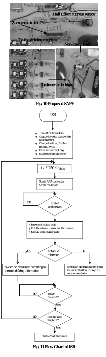
We can summarize the program of the experimental work in the flow chart of Fig. (11).
IV. EXPERIMENTAL RESULTS
Fig. (6) shows the experimental results of the proposed series active power filter supply voltage and current before filtering (we observe the current and the voltage of the load without any filtration). Fig. (7) shows the experimental results of the proposed series active power filter supply voltage and current after filtration. The current after filter approaches the sinusoidal shape, it is in-phase with the supply voltage, and that proves the validity of the proposed filter. Similarly, in Fig. (8) and (9) we show the variation of the load current before and after filtration by adjusting the variable potentiometer of the current sensor. We can use this controller for different type and values of non-linear load currents.
The reference current is 0.9 A peak the fundamental of the load current.
Note: during experiment we measure i across 2.2Ωseries resistor then the exact value of the maximum obtained when we divide by the scale which is 2.22
TABLE 1
PARAMETERS OF THE SAPF
Supply voltage vs 110v
Frequency f 50Hz
Load resistor R 33Ω
Load capacitor C 40μf
Limiter L 100mH
Filter capacitance Cdc 2000μf
V. CONCLUSION
can conclude that the total harmonic distortion decreases by 25-30%. Within a certain limits, it is also capable of correcting fundamental voltage amplitude as in Fig. (7) the voltage of the main becomes totally sinusoidal while in Fig. (6) the distortion in the main voltage is very clear. Although the tested series compensator was a single-phase version, it may be easily adapted to a three-phase system. A series active power filter, working as a sinusoidal current source, in phase with the mains voltage, has been developed and tested. The amplitude of the fundamental current in the series filter is controlled through the microcontroller or PIC16f788 between the load voltage and a pre-established reference. The control allows an effective correction of power factor, harmonic distortion, and load voltage regulation and reaching its steady state in about two cycles of the fundamental. Compared with other methods of control for a series filter, this method is simpler to implement, because it is only required to generate a sinusoidal current, in phase with the mains voltage, the amplitude of which is controlled through the proposed cheep circuit [8], [9].
-Zero cross to the Pic
to
To the driving circuit
Hall Effect current sensor
To inverter bridge
Non-linear load
ISR
• Turn off all transistors
• Change the edge state for the next interrupt
• Change the firing for this new half cycle
• Clear the interrupt flag
• Set the lookup table to 0
s t=250μ
Δ delay
Starts A/D converter Starts the timer
End of conversion
•Increment lookup table
•Call the reference value for this current
•Sample from lookup table
Actual < reference
Switch on transistors according to the stored firing information
Switch off all transistors to force the current to flow through the appropriate diodes
Timer finished??
Turn off all transistors Lookup table finished??
no
no yes
no
no
yes
yes i (1v/div)
V (50v/div)
10ms/div
R=33Ω, C=40μf
[image:4.595.314.536.45.790.2]R=33Ω, C=25μf
Fig. 6 Source Voltage and Line Current of Uncompensated Circuit
i
v
[image:4.595.43.283.296.383.2]
5m s/ di v R= 3 3 Ω, C = 40μf
Fig. 7 Source Voltage and Source Current After compensation
R = 33Ω, C= 2 5μ f
[image:4.595.45.283.394.483.2]
Fig. 8 Source Voltage and Line Current of Uncompensated Circuit
Fig. 9 Source Voltage and Source Current of Compensated Circuit
Fig. 10 Proposed SAPF
[image:4.595.47.281.513.598.2] [image:4.595.45.283.632.725.2]ACKNOWLEDGEMENTS
The author would like to thank Prof. Amer El-zwawe for their help in this work. The authors are grateful to HCU University for the great help in all steps.
REFERENCES
[1] H. Akagi, ‘‘New Trends in Active Filters for Power Conditioning”, IEEE Trans. Ind. Appl. 1996, 32, (6), pp. 1312-1322.
[2] Afonso, J., and et.al, “Active Filters with Control Based on the p-qTheory” IEEE Industrial Electronics Society Newsletter, Vol.47, No.3,pp. 5-11, 2000.
[3] Magureanu R., Ambrosii S., Creanga D., Staicu C., Radut V. (2002) “Unity power factor rectifiers andactive power filters for industrial applications”, Proceedings – National Conference on Electrical Drives,Galati.
[4] A.M. Massoud, S. J. Finney, B. W. Williams, “Review of harmonic current extraction techniques for an active power filter” IEEE international conference on harmonics and quality of power 2004: 154-159
[5] Katsumi Nishida, Md. Rukonuzzaman and Mutsuo Nakaoka. “A novelsingle-phase shunt active power filter with adaptive neural network based harmonic detection” IEEJ Trans. LA, 2005; Vol. 125, N0. 1: 9-
[6] A current limiter based on an active current power filter Vazquez, N. Rico, D. Hernandez, C. Rodriguez, E. Orosco, R. Arau, J. Power Electronics Congress, 2008. CIEP 2008. 11th IEEE International Publication no. 5, pp. 51-55 Aug. 2008
[7] M.Rashid. Power Electronics Circuits, Devices and Applications. Pearson Prentice Hall, 2003.
[8] V. B. Sriram, S. SenGupta and A. Patra, "Indirect current control of a single-phase voltage-sourced boost-type bridge converter operated in the rectifier mode," IEEE Trans. Power Electron., vol.18, no. 5, pp. 1130-1137, Sep. 2003.
[9] M. Basu, S. P. Das and G. K. Dubey, "Parallel converter scheme for high-power active power filters," IEE Proc. Electr. Power Appl.,vol. 151, no. 4, pp. 460-466, July 2004.
[10] Y. S. Kim, J. S. Kim and S. H. Ko, “Three-PhaseThree-Wire Series Active Power Filter, which Compensates for Harmonics and Reactive Power”,IEE proc. Electr. Power Appl., Vol, 151, no. 3, May 2004, pp. 276-282.
[11] S. P. Litrán, P. Salmerón, J. R. Vázquez and R. S.Herrera, “Different control strategies applied toseries active filters”, in Proc. ICREPQ, May, 2007
[12] M. João Sepúlveda, João L. Afonso and Júlio S. Martins, “A Series Active Filter Controlled by Personal Computer”, International Conference on Renewable Energy and Power Quality (ICREPQ’03), Vigo, Spain, 9-12 April 2003.
[13] J. Jerzy and F. Ralph, “Voltage waveshape improvement by means of hybrid active power filter,” in Proc. IEEE ICHPS VI, Bologna, Italy, Sept. 21–23, 1994, pp. 250–255.
(Modified on 15-9-2009 and the modifications include 1- The personal details at the footnote
2- The description of figure 13)
R1 1k R2 10k 1M 3 2 1 4 1 1 LM324 BR1 2W01G 3 4 1 2 CURRENT SENSOR 15v -15v 500K POT 1M D3 1M130ZS5 1 2 J1
to MCU Hall effect input
RA0/AN0 2 RA1/AN1 3 RA2/AN2/VREF-4 RA4/T 0CKI 6 RA5/AN4/SS 7 RE0/AN5/RD 8 RE1/AN6/WR 9 RE2/AN7/CS 10 OSC1/CLKIN 13 OSC2/CLKOUT 14
RC1/T 1OSI/CCP2 16 RC2/CCP1 17 RC3/SCK/SCL 18 RD0/PSP0 19 RD1/PSP1 20 RB7/PGD40 RB6/PGC39 RB5 38 RB4 37 RB3/PGMRB2 3635 RB1 34 RD7/PSP7 30 RD6/PSP6 29 RD5/PSP5 28 RD4/PSP4 27 RD3/PSP3 22 RD2/PSP2 21 RC7/RX/DTRC6/T X/CK 26 25 RC5/SDO 24 RC4/SDI/SDA 23 RA3/AN3/VREF+ 5
RC0/T 1OSO/T1CKI 15 MCLR/Vpp/THV 1 RB0 33 PIC16F877 4MHZ 22pf 22pf R1 10k VI 1 VO3
G N D 2 7805 470uf 470uf 220nf 220nf + - 12v 5v 5V 6 5 4 1 2 U1 4N25 R2 100k R3 10k ZERO CROSSING 1 2 3 4 5 GND MCU_D MCU_C MCU_B MCU_A MOSFET DRIVER 1 2 HALL-EFFECT H-E GND NEUTRAL PHASE 6 5 4 1 2 U1
OPT OC OU PL ER - N PN
1 2 3 4 J1
C ON N - H 4
12V 5V MC U _ A
G N D
330 3 2 5 4 7 6 9 10 404 9 1k Q1
IR F 740
6 5 4 1 2 U3
OPT OC OU PL ER - N PN
1 2 3 4 J2
C ON N - H 4
12V 5V MC U _B
G N D
R3 330 11 12 14 15 3 2 5 4 404 9 1k Q2
IR F 740
6 5 4 1 2 U5
OPT OC OU PL ER - N PN
1 2 3 4 J3
C ON N - H 4
12V 5V MC U _C
G N D
R5 330 7 6 9 10 11 12 14 15 404 9 1k Q3
IR F 740
6 5 4 1 2 U6
OPT OC OU PL ER - N PN
1 2 3 4 J4
C ON N - H 4
12V 5V MC U _D
G N D
R7 330 3 2 5 4 7 6 9 10 404 9 1k Q4
IR F 740
[image:5.595.49.278.53.510.2]N E U TR AL P H AS E
Fig. 14 Non linear Load Harmonics of the Compensated System
Frequency (kHz) Frequency (kHz) Curren t ( A )
[image:5.595.317.535.70.180.2]Fig. 12 Over All Control Schematic Diagram
Fig. 13 Load Harmonics of Uncompensated System
[image:5.595.49.259.558.683.2]